Journal of Modern Physics
Vol. 2 No. 8 (2011) , Article ID: 6821 , 7 pages DOI:10.4236/jmp.2011.28102
Structural and Electronic Properties of Impurities on Boron Nitride Nanotube
1Departamento de Tecnologia Química, Universidade Federal do Maranhão, São Luis, Brazil
2Departamento de Física, Universidade Federal do Maranhão, São Luis, Brazil
E-mail: silvete@pq.cnpq.br
Received May 2, 2011; revised June 18, 2011; accepted June 28, 2011
Keywords: BN Nanotube, DFT, Electronic Properties
ABSTRACT
The structural and electronic properties of molybdenum and magnesium substitution doping in (10,0) boron nitride nanotube (BNNT), are investigated through first-principle calculations. The electronic band structures results indicate that the molybdenum doped systems behave as n-type impurity. However, the magnesium doped systems behave as p-type impurity when magnesium replaces boron, and as an n-type impurity when the magnesium replaces nitrogen. The analysis of the energies formation shows that the molybdenum replacing a boron and nitrogen atoms are more favorable than the magnesium substitution in boron and nitrogen.
1. Introduction
Boron nitride nanotubes (BNNTs) which are known to be wide gap semiconductors with band gaps about 5.5 eV [1,2] and in their native state are essentially electrical insulating. The form zigzag structure BNNTs are more stable than their carbon counterparts in terms of thermal and chemical stability. The other advantage about BNNTs is that they don’t require the choice of a specific chirality due to the invariance of optical and electronic properties from case carbon nanotubes. This makes the BNNTs superior to carbon nanotubes for a series of optoelectronic applications. The BNNTs also possess high surface area, unique physical properties, and morphology. Their inherent size and hollow geometry can make them extremely attractive as supports for heterogeneous catalysts [3-7]. Chemical inertness and a strong resistance to oxidation, for example, make BNNTs highly appropriate for the construction of insulating nanocables, a subject that has been attracting increased attention [8-10].
Many properties of semiconductor devices are derived from the presence of doping, which is an effective way to control and improve the source side injection of carriers into conventional semiconductors. Hence, the possible implementations of BNNTs based devices require the study of suitable defects and impurities that could act as an electron/or hole. For example, Zhao et al. in theoretical results show to the possibility of transforming the insulating BNNT into a n-type or a p-type semiconductor by carbon-doping for the case of C substituting for B or N atom respectively [7]. Tang et al. in experimental work demonstrates a novel route for fluorine-doping, where the fluorine was suggested to occupy the nitrogen site in the nanotube and yielded an n-type semiconductor [8].
In this work we study the doping of BNNT with molybdenum (Mo) and magnesium (Mg) using firstprinciple method based on density functional theory. The reason we choose Mo atom doping is that transition metal atoms are commonly present during the synthesis of BN nanostructure carrying formation of BN nanostructures doped with transition metals atoms [11], while the Mg atom is frequently considered for creating p-type conductivity in BN compound [12]. The structure was first relaxed and then electronic properties were obtained. The incorporation of the Mo and Mg are explored as substitutions for B and N atoms. It is shown that incorporation of Mo atom in a B and N site has low formation energy and that the electronic band structure indicates that energy gap decrease when Mo and Mg impurities are introduced in the pristine BNNT.
2. Method of Calculation
First principle density functional theory [13] has been employed to investigate the Mo and Mg substitution atoms in the B (MoB and MgB) and the N (MoN and MgN) sites of the (10,0) BN nanotubes. We used the Siesta code [14], which performed full self consistent calculations solving the Kohn Sham equations [15] and using numerical atomic orbital as basis sets. In all calculations we used a split valence double zeta basis set with polarization function [16]. For the exchange and correlations terms we use the generalized gradient approximation with the parameterization of Perdew-Burke-Ernzerhof [17]. The interaction between ionic cores and valence electrons is described by norm conserving pseudopotentials [18] in Kleinamn-Bylander form [19]. A cutoff of 150 Ry for the grid integration was used to represent the charge density. The Brillouin zone is sampled with eighteen k points special along the Γ-X directions used Monkhorst-Pack method [20].
Our calculations were performed using a (10,0) BN nanotubes. Periodic boundary conditions and a supercell approximation with a lateral separation of 40 Å between tube centers are used to ensure that the nanotubos plus atom dopant do not interact with their images. The supercell were used have 80 atoms, with a total length of 8.58 Å. The impurities atoms were incorporated as a substitution (Mo and Mg)-atom in the nanotube and a fully relaxation was performed using the Hellmann-Feynman forces with a Pulay-like correction. The structural optimizations were performed using a conjugated gradient procedure, and atomic positions of the structure were relaxed up to the point of obtaining all force components smaller than 0.05 eV/Å.
3. Results and Discussion
In study the structural properties of the Mo-doped in (10,0) BNNT, we find that the local symmetry of the nanotube breaks up after relaxation and it undergoes a Jahn-Teller distortion [21]. The Figures 1(a) and (c) shows the resulting relaxed structure of the (10,0) BNNT with a Mo substitution atom in site B (MoB) and in site N (MoN), respectively. While in Figures 1(b) and (d) some of the atoms are numbered in order to describe the relevant structural parameters. In Tables 1 and 2, some inter atomic distances and angles are listed for the MoB and MoN substitution, respectively. In Figure 1(a) the Mo atom is displaced 0.88 Å out of the original position, while in Figure 1(c) the Mo atom is displaced by 1.11 Å. The distances between the atom 1 and its first N neighbors (Figures 1(a)-(b)) are 2.08 Å, which is in agreement with the results (2.07 Å) of Gajbhiye and Ningthoujam [22]. The distances the atom 1 and its first B neighbors (Figures 1(c)-(d)) are 2.38 Å, which are consistent with the results (2.48 Å) of Nakazawa et al. [23].
The Figure 1(e) shows the resulting optimized struc-
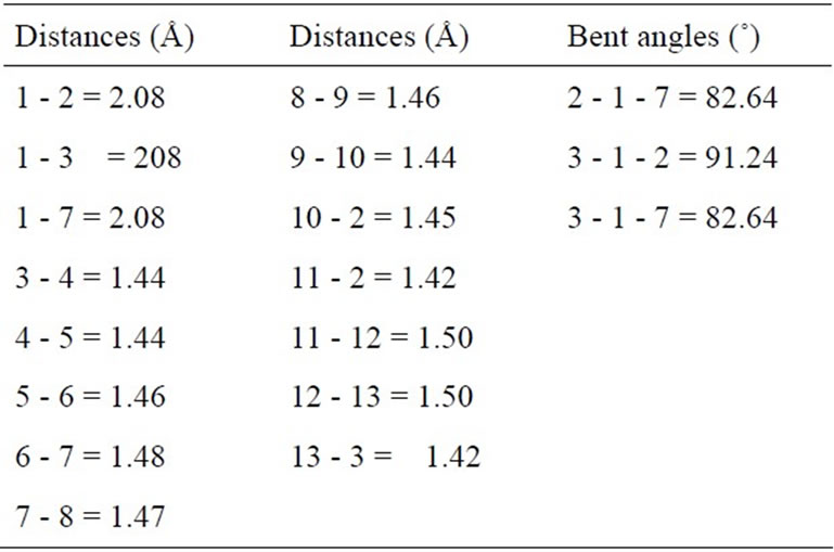
Table 1. Structural parameters for the MoB-doped BN nanotube. The numbers identifying the distances and angles refer to Figure 1(b).
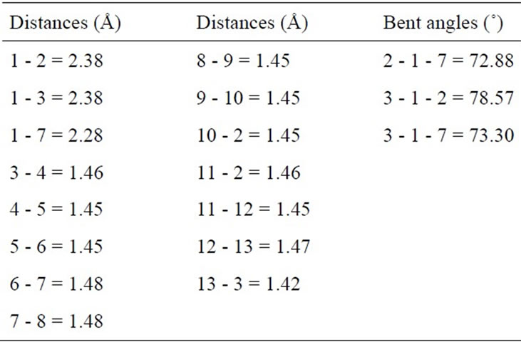
Table 2. Structural parameters for the MoN-doped BN nanotube. The numbers identifying the distances and angles refer to Figure 1(d).
tures in the doped (10,0) BNNT with an Mg substitution atom in B-site (MgB), and Figure 1(f) shows some atoms are numbered in order to describe the relevant distance. In Table 3, inter atomic distances and angles are listed for the MgB substitution. The distances between the atom 1 and its first N are 1.98 Å for the Mg-N distance quasi-collinear with the axis, and 2.00 Å for Mg-N distances where N atoms are related by a mirror plane containing the Mg atom and nanotube axis. As compared to the distances in Mg3N2, where these distances vary from 2.08 Å to 2.18 Å [24], a very small enlargement is observed. The relaxed structural configuration of the MgN system is shown in Figure 1(g). In Figure 1(h), some of the atoms are numbered in order to describe the relevant structural parameters. In Table 4 inter atomic distances are listed for the MgN system. The Mg atom moves out of tube axis, leaving a vacancy and forming a wrong B-B bond of 1.95 Å. The distances between the 1-2, 1-3 and 1-7 atoms are 2.35 Å, 2.73 Å and 3.12 Å, respectively. These values are much different than the Mg-B distance that is of the order 2.23 Å and 2.53 Å of the ab initio calculation by Yang et al. [25].
Electronic band structure near the Fermi level were
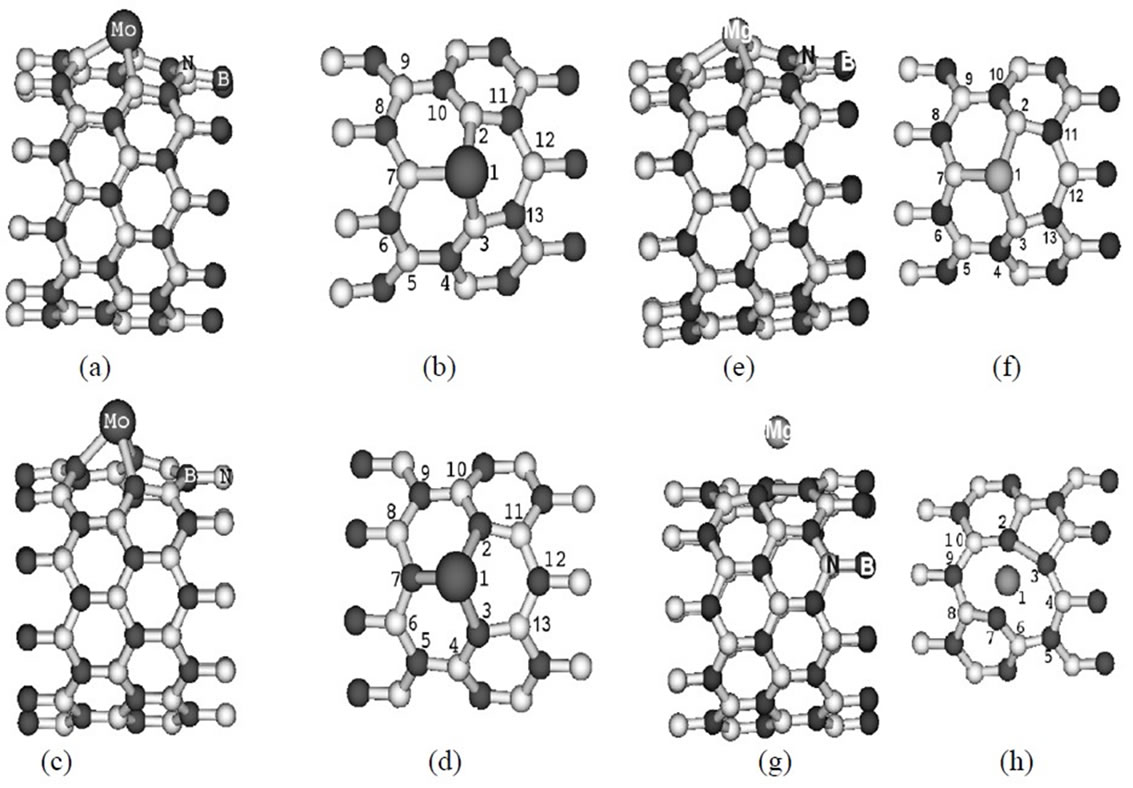
Figure 1. Relaxed structure representation for BN nanotube with and Mo [Mg] substitution atom in: (a)-(b) [(e)-(f)] B site and (c)-(d) [(g)-(h)] N site. The atoms are represented by atomic symbol.
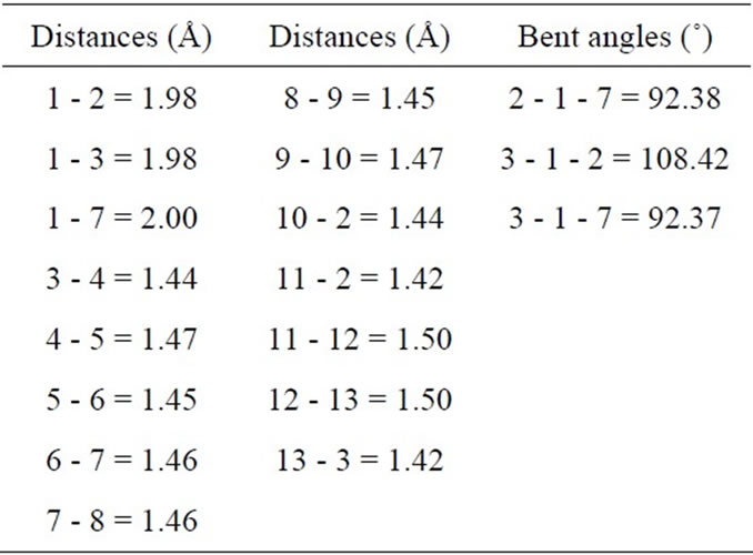
Table 3. Structural parameters for the MoB-doped BN nanotube. The numbers identifying the distances and angles refer to Figure 1(f).
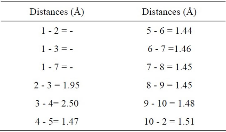
Table 4. Structural parameters for the MoB-doped BN nanotube. The numbers identifying the distances and angles refer to Figure 1(f).
obtained for the doped nanotubes in situations MoB, MoN, MgB and MgN. The band structure for the pristine (10,0) BNNT is shown in Figure 2(a). The band gap of 4.05 eV is in good agreement with those calculated for nanotubes with diameters ≥ 14.0 Å in literature [26,27]. The results indicate the (10,0) BNNT to behave as a wide band gap semiconductor or insulator. The Fermi level is represented by the dashed line. The Figures 2(b) and (c) shown the band structure for the majority (spin-up) and minority (spin-down) carriers, respectively. We can observed that the Fermi level of the MOB system is shifted 1.26 eV up compared with that of the pristine (10,0) for both majority and minority electronic bands. By comparison with the pristine BNNT we can observe that the Mo-doped introduces levels relatively flat in gap region. The band structure for the majority state (Figure 2(b)) shows that the localized level is located at about 0.59 eV above the top valence band and almost localized level at about 0.57 eV below the bottom of the conduction band. While that the band structure for the minority state (Figure 2(c)) shows that three deep levels emerge into the band gap and another one at the bottom of conduction band. Two of the deep gap states are semioccupied and two are empty. The semioccupied levels are located at about 0.3 eV and 2.76 eV above the top of the valence band, respectively. The empty levels at about 1.00 eV and 0.21 eV below the bottom of the conduction band, respectively. By substituting the N for Mo in the pristine tube the band structure changes, as show the Figures 2(d) and (e), which represent the spin-up and spin-down band structure, respectively. The Fermi level is shifted up, 0.36 eV, compared to undoped (10,0) BNNT. Other change in MoN is that several almost localized levels appear in gap region are all centered on the Mo impurity atom. The band structure for the spin-up level shown the unoccupied level 0.24 eV above the Fermi energy and the occupied level 0.23 eV below the Fermi energy. On
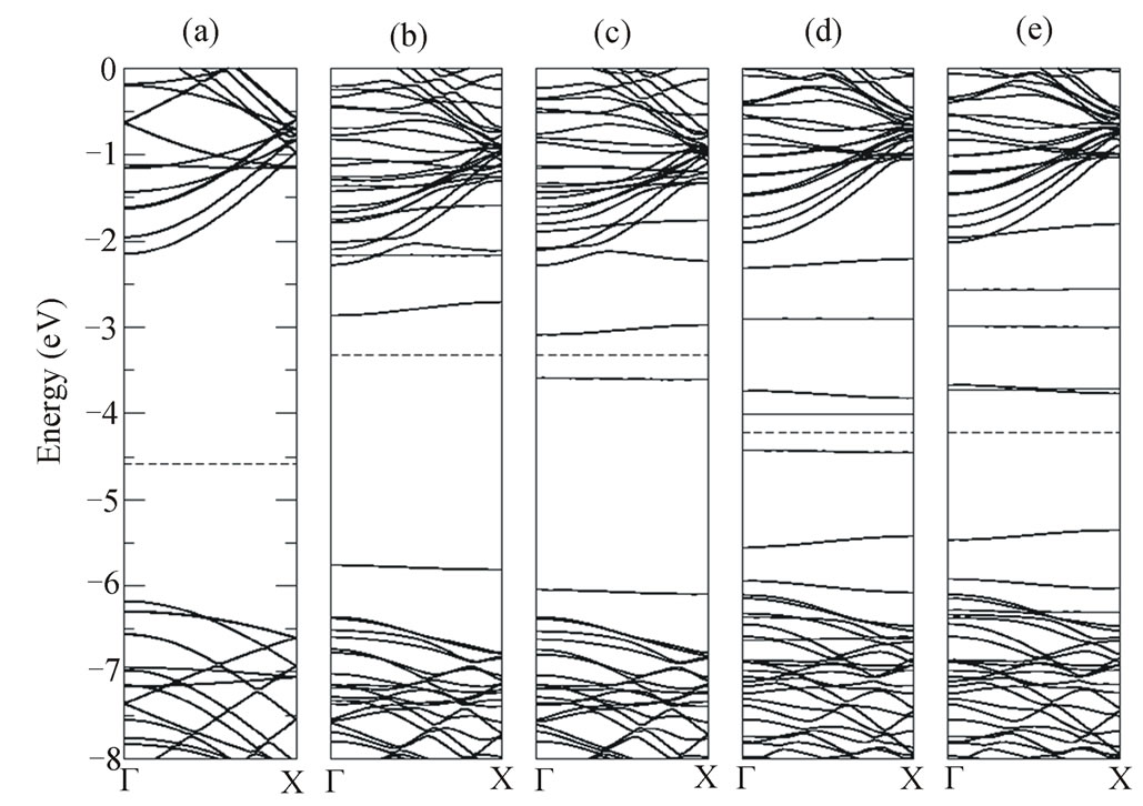
Figure 2. Calculated electronic band structure for: (a) (10,0) BNNT, (b) spin-up electrons MoB defect, (c) spin-down electrons MoB defect, (d) spin-up electrons MoN defect, and (e) spin-down electrons MoN defect. The Fermi energy is indicated by dashed line.
the other hand, the band structure for the spin-down level shows the occupied level 1.28 eV below the Fermi energy and the unoccupied level 0.5 eV above the Fermi level. The energy gap between the highest occupied molecular orbital (HOMO), lowest, and the unoccupied molecular orbital (LUMO) of the Mo-doped BNNTs is 0.51 eV for MoB and 0.42 eV for MoN. In both MoB and MoN systems the Fermi level shifts up to the conduction band due to the charge transfer from tube to the Mo atom. These systems behave as a semiconductor n-type.
The spin-up and spin-down band structure for the MgB system is shown in Figures 3(b) and (c), respectively. The Figure 3(a) presented, for comparison, the band structure for the isolated (10,0) BNNT. The Mg doping moves the Fermi energy towards the valence band thus indicating the Mg is acting as an electron acceptor. The change more significant in the band structure for majority states (Figure 3(b)) occurs in the gap region, where we can observe that three deep levels emerge into the band gap. We can observed that the first level below the Fermi energy present the dispersion energy around 0.25 eV along the Γ-X direction and, thus suggesting a delocalized character. On other the hand, the first level above the Fermi energy is relatively flat, with dispersion energy around 0.15 eV along the Γ-X direction that suggests a localized character. The other flat level is localized at 2.98 eV above the Fermi energy. The band structure for the minority states (Figure 3(c)) shows that the principal change is that one flat level appears 2.97 eV above the Fermi гenergy and new levels appear in the valence band and conduction band. The Figure 3(d) and (e) show the spin-up and spin-down band structure, respectively. Unlike what happens with the Mg atom replacing an atom of B, replacing the N atom by atom of Mg causes the Fermi level to move to the conduction band. We infer that the difference between the two systems must occur due to the fact of structural relaxation after a vacancy arises, since the Mg atom does not remain connected to the tube. The Fermi level shifts (1.18 eV) to the bottom conduction band due to the insertion of the impurity. If observing the band structure for spin-up (Figure 3(d)) shows that the localized level appears in 0.44 eV below the Fermi level. Also, we observed one level relatively flat at approximately 2.01 eV below Fermi level with an energy dispersion, in direction Γ-X, around 0.10 eV. The other around level rises in ~1.03 eV above the Fermi level with an energy dispersion around 0.10 eV in Γ-X direction. The around value 0.10 eV from dispersion energy suggests a localized character. Finally, the Figure 3(e) shows the band structure for spin-down, where it can be observed that again a relatively flat level appears in gap region. One level is localized 1.61 eV below the Fermi level with the dispersion energy the 0.11 eV, while two levels are localized in 0.45 eV and 1.06 eV above the Fermi level, with dispersion energy the 0.11 eV and 0.05 eV in Γ-X direction, respectively. By comparison, with the (10,0) BNNT in the both band structure spin-up and spin-down, new levels emerge in top valence band and bottom of the conduction band. In the MgB and MgN defects, the difference between the HOMO and the LUMO are 0.18 eV and 0.86 eV, respectively.
Another aspect interesting to explore is the preferential site for doped position. In principle, the Mo should substitute boron preferentially, due to their closer electronegativity. This is further confirmed by calculating the formation energy (Eform). Dopants Table 5 presents the
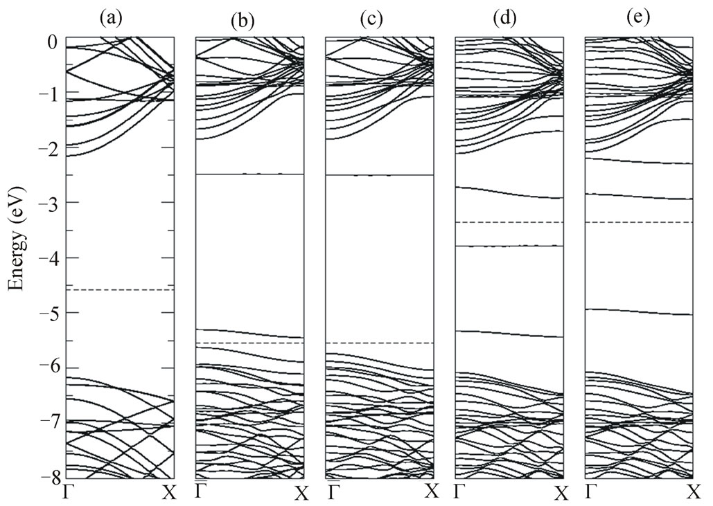
Figure 3. Electronic band structure of (a) (10,0) BNNT, (b) spin-up band MgB defect, (c) spin-down band MgB defect, (d) spin-up band MgN defect, and (e) spin-down band MgN defect. The Fermi energy is indicated by dashed line.
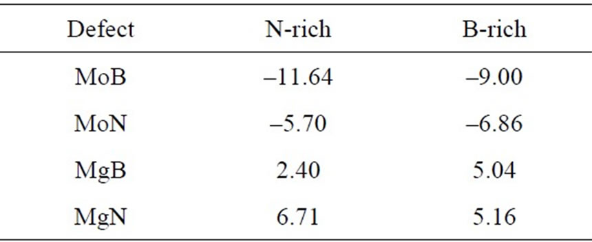
Table 5. Calculated formation energies (in eV) for MoB, MoN and MgB in B-rich and N-rich conditions.
formation energy (Eform) of the molybdenum and magnesium substitution the system (10,0) BNNT in B-rich and N-rich conditions. The formation energy is calculated through the expression:
Eform = E[Tube + D] – nNμN – nBμB – nDμD (1)
where E[Tube+D] is the total energy of D(Mo,Mg)doped nanotube, n is the number of atoms (B, N, Mo, and Mg) and μ is a chemical potential. The chemical potentials for B and N atoms must also obey the equilibrium condition [28].
μBN[tube]= μN + μB(2)
The chemical potentials μN, μB, μMo, and μMg, which are calculated as the total energy per atom of the more stable configurations: the cubic Mo bulk, Mg hexagonal bulk, α-B bulk, and N2 molecule, respectively. All these calculations are performed using the same procedure as employed to the study of the Mo and Mg substitution impurities. Two extreme conditions can be specified defining the foreign species as either an N-rich or a B-rich environment. For the B-rich conditions, the μN, is calculated using 2 by taking μB as a fixed parameter. On the other hand, for an N-rich condition, μB is calculated using 2 with the μN taken as fixed.
Table 5 lists the calculated values for formation energies in both N-rich and B-rich conditions of the (Mo,Mg)- doped BNNT. The comparison of the results in terms of the formation energy from the Mo and Mg are interesting. We observe that the system with a doped Mo atom presents negative formation energy. Indicating that it is relatively easy to incorporate a Mo atom in the BNNT in both B-rich and N-rich conditions. The calculated values for the formation energies in both B-rich and N-rich conditions of the Mg-doped BNNT (see Table 5) shows that the formation energies are higher in the MgN replacement. Indicating a greater probability for Mg to replace the boron atom than the nitrogen atoms.
Examination the band gap it is seen that the defective systems alter the (10,0) BN nanotube band gap. On the other hand, the presence of defective levels in the band gap completely changes the optical and electronic behaviors of these systems. The band structure of the low formation energy MoB defect turns it possible to be identified by optical experiments once transitions from the level in the gap should require much lower energies than the nanotube intrinsic transitions.
4. Conclusions
In summary, (Mo and Mg)-doped in a (10,0) BNNT were studied using the first principle calculations, based on the density functional theory. For the possibilities, MoB, MoN and MgB, significant outward radial relaxations of the Mo and Mg atoms are observed, resulting in (Mo and Mg)-first neighbors distances similar to those found in literature in compounds involving B and N atoms. For the MgN system a vacancy is formed in (10,0) BNNT with replace of Mg atom in place of N atom. The band structure shows that new levels appear in gap region and these levels are centered on the Mo and Mg impurity. Also, the difference between HOMO and LUMO is diminished when the Mo and Mg atoms are replaced in the pristine tube being that smallest difference between the HOMO and LUMO is observed in the MoN system whose value is 0.42 eV. The results for the formation energies indicate that the configuration more favorable energetically where the B (N) substitution by a Mo atom, especially for the N-rich situation in MoB configuration.
5. Acknowledgements
We thank the CENAPAD-SP for computer faciliteis, and Desenvolvimento Científico e Tecnológico do Maranhão, FAPEMA, and the Conselho Nacional de Desenvolvimento Científico e Tecnológico, CNPq, for financial support.
REFERENCES
- N. G. Chopra, R. J. Luyken, K. Cherrey, V. H. Crespi, M. L. Cohen, S. G. Louie and A. Zettl, “Boron-Nitride Nanotubes,” Science, Vol. 269, No. 5226, 1995, pp. 966-967. doi:10.1126/science.269.5226.966
- A. Rubio, J. L. Corkill and M. L. Cohen, “Theory of Graphitic Boron Nitride Nanotubes,” Physical Review B, Vol. 49, No. 7, 1994, pp. 5081-5084. doi:10.1103/PhysRevB.49.5081
- M. Terrones, “Carbon Nanotubes: Synthesis and Properties, Electronic Devices and Other Emerging Applications,” International Materials Reviews, Vol. 49, No. 6, 2004, 325-377. doi:10.1179/174328004X5655
- J. J. Gooding, “Nanostructuring Electrodes with Carbon Nanotubes: A Review on Electrochemistry and Applications for Sensing,” Elextrochimica Acta, Vol. 50, No. 15, 2005, pp. 3049-3060. doi:10.1016/j.electacta.2004.08.052
- C. A. Dyke, J. M. Tour, “Covalent Functionalization of Single-Walled Carbon Nanotubes for Materials Applications,” Journal of Physical Chemistry A, Vol. 108, No. 51, 2004, pp. 11151-11159. doiv10.1021/jp046274g
- M. S. Dresselhaus, G. Dresselhaus and A. Jorio, “Unusual Properties and Structure of Carbonnanotubes,” Annual Review of Materials Research, Vol. 34, No. 1, 2004, pp. 247-278. doi:10.1146/annurev.matsci.34.040203.114607
- J.-X. Zhao and B.-Q. Dai, “DFT Studies of ElectroConductivity of Carbon-Doped Boron Nitride Nanotube,” Materials Chemistry and Physycs, Vol. 88, No. 2-3, 2004, pp. 244-249. doi:10.1016/j.matchemphys.2003.10.018
- C. Zhi, Y. Bando, C. Tang and D. Golberg, “Immobilization of Proteins on Boron Nitride Nanotubes,” Journal of the American Chemical Society, Vol. 127, No. 49, 2005, pp. 17144-17145. doi:10.1021/ja055989+
- S. Chopra, A. Pham, J. Gaillard, A. Parker and A. M. Rao, “Carbon-Nanotube-Based Resonant-Circuit Sensor for Ammonia,” Applied Physics Letters, Vol. 80, No. 24, 2002, pp. 4632-4634. doi:10.1063/1.1486481
- C. Zandonella, “Is It All Just a Pipe Dream?” Nature, Vol. 410, No. 6830, 2001, pp. 734-735. doi:10.1038/35071183
- X. Wu and C. Zeng, “Adsorption of Transition-Metal Atoms on Boron Nitride Nanotube: A Density-Functional Study,” Journal of Chemical Physics, Vol. 125, No. 4, 2006, pp. 044711-1-044711-7. doi:10.1063/1.2218841
- J. H. Edgar, “Prospects for Device Implementation of Wide Band-Gap Semiconductors,” Journal of Materials Research, Vol. 7, No. 1, 1992, pp. 235-252. doi:10.1557/JMR.1992.0235
- P. Hohenberg and W. Kohn, “Inkomogeneous Electron Gas,” Physical Review B, Vol. 136, No. 3B, 1964, pp. 864- 871. http://dx.doi:10.1103/PhysRev.136.B864
- P. Ordejon and J. M. Soler, “Self-Consistent Order-N Density-Functional Calculations for Very Large Systems,” Physical Review B, Vol. 53, No. 16, 1996, pp. 10441- 10444. doi:10.1103/PhysRevB.53.R10441
- W. Kohn and L. J. Sham, “Self-Consistent Equations Including Exchange and Correlations Effects,” Physical Review, Vol. 140, 1995, pp. 1133-1138. doi:10.1103/PhysRev.140.A1133
- E. Artacho, D. Sachez-Portal, P. Ordejon, A. Garcia and J. M. Soler, “Linear-Scaling Ab-Initio Calculations for Large and Complex Systems,” Physica Status Solidi B-Basic Research, Vol. 215, No. 1, 1999, pp. 809-817. doi:10.1002/(SICI)1521-3951(199909)215:1<809::AID-PSSB809>3.0.CO;2-0
- J. P. Perdew, E. Burke and M. Ernzerhof, “Generalized Gradient Approximation Made Simple,” Physical Review Letters, Vol. 77, No. 18, 1996, pp. 3865-3868. doi:10.1103/PhysRevLett.77.3865
- N. Troullier and J. L. Martins, “Efficient Pseudopotencials for Plane-Wave Calculations,” Physical Review B, Vol. 43, No. 11, 1991, pp. 1993-2006. doi:10.1103/PhysRevB.43.1993
- L. Kleinman and D. M. Bylander, “Efficacious Form for Model Pseudopotentials,” Physical Review Letters, Vol. 48, No. 20, 1982, pp. 1425-1428. doi:10.1103/PhysRevLett.48.1425
- H. J. Monkhorst, J. D. Pack, “Special points for Brillouin-Zone Integrations,” Physical Review B, Vol. 13, No. 12, 1976, pp. 5188-5192. doi:10.1103/PhysRevB.13.5188
- M. Fujita, K. Wakabayashi, K. Nakada and K. Kusaka, “Peculiar Localized State at Zigzag Graphite Edge,” Journal of the Physical Society Japan, Vol. 65, No. 7, 1996, pp. 1920-1923. doi:10.1143/JPSJ.65.1920
- N. S. Gajbhiye and R. S. Ningthoujam, “Structural, Electrical and Magnetic Studies of Nanocrystalline δ-MoN and γ-Mo2N,” Physica Status Solidi A, Vol. 1, 2004, pp. 3449-3454.
- H. Nakazawa, M. Itazaki and M. Ohba, “Molybdenum Complexes Bearing a Diaminosubstituted-Phosphiteboryl Ligand: Syntheses, Structures, and Reactivity Involving the Mo-B, B-P, and B-H Activation,” Journal of Organometallic Chemistry, Vol. 692, 2007, pp. 201-207. doi:10.1016/j.jorganchem.2006.04.049
- C. M. Fang, R. A. de Groot, R. J. Bruls, H. T. Hintzen and G de With, “Ab Initio Band Structure Calculations of Mg3N2 and MgSiN2,” Journal Physical: Condenser Matterial, Vol. 11, No. 25, 1999, pp. 4833-4842. doi:10.1088/0953-8984/11/25/304
- C.-L. Yang, X. Zhangb and K.-L. Hanb, “Ab initio Geometries, Electronic Structures of MgB2 Molecule,” Journal of Molecular Structure-Theochem, Vol. 677, No. 1-3, 2004, pp. 11-14. doi:10.1016/j.theochem.2004.01.041
- G. Guo and J. Lin, “Systematic Ab Initio Study of the Optical Properties of BN Nanotubes,” Physical Review B, Vol. 71, No. 16, 2005, pp. 165402-1-165402-12. doi:10.1103/PhysRevB.71.165402
- X. Blase, A. Rubio, S. Louie, M. Cohen, “Stability Constancy of Boron-Nitride Nanotubes,” Europhysics Letters, Vol. 28, pp. 335-340. doi.org/10.1209/0295-5075/28/5/007
- J. E. Northrup, S. B. Zhang, “Dopant and Defct Energetics-Si in GaAs,” Physical Review B, Vol. 47, No. 11, 1993, pp. 1484-1492. doi:10.1103/PhysRevB.47.6791