Advances in Chemical Engineering and Science
Vol.3 No.1(2013), Article ID:27043,7 pages DOI:10.4236/aces.2013.31013
Optical-Electronic Properties of Carbon-Nanotubes Based Transparent Conducting Films
1Department of Chemical Engineering, National Tsing Hua University, Hsinchu, Chinese Taipei
2Material and Chemical Laboratory, Industrial Technology & Research Institute, Hsinchu, Chinese Taipei
3Department of Chemical Engineering, Monash University, HHMelbourneHH, Australia
Email: *tjliu@che.nthu.edu.tw
Received October 12, 2012; revised November 13, 2012; accepted November 22, 2012
Keywords: Carbon Nanotubes; Transparent Conductive Film; Dip Coating; Slot Die Coating; Blade Coating; Sheet Resistance; Transparency
ABSTRACT
Three coating methods (slot, dip and blade coatings) were used separately to coat a well-dispersed single-wall carbonnanotube (SWCNT) solution on polyethylene terephthalate (PET) film, and the resulting optical and electronic properties were measured and compared. It was found that the sheet resistance and the transparency of the SWCNT coated film decreased as the coating speed increased for dip and blade coatings, but were independent of the coating speed for slot coating. All three coating methods were able to produce transparent conductive film with transparency above 85% and sheet resistance close to 1000 ohm/sq. For industrial production, the slot die coating method appears to be more suitable in terms of high coating speed and uniformity of optical and electronic properties.
1. Introduction
Transparent conductive film or glass is a key component for many optical-electronic devices such as organic light emitting diodes (OLED), organic photovoltaic solar cells (OPV), liquid crystal display (LCD) panels and touch panels, just to name a few. The most critical requirements for transparent conductive film or glass are low sheet resistance and high transparency. Many materials were considered suitable for making transparent conductive film or glass [1-4]. Owing to manufacturing and quality requirements, only indium tin oxide (ITO) film or glass has been commonly used for optical-electronic devices in the current market [5]. Despite its popularity, indium is a rare-earth material, and its price is high [6]. Furthermore, ITO films or glass has to be produced with a vacuum deposition technology. This technology is relatively expensive compared to conventional wet coating processes. Hence, many competitive approaches have been sought to replace ITO film or glass using different materials and coating methods.
Low-cost wet coating processes have been found to be promising in coating nano-scaled conductive media such as silver nanowires [7] or carbon-nanotubes [8-11] on PET film. Silver nanowires can be produced through an efficient chemical approach [12]. However, issues such as how to disperse silver nanowires and reduce their diameter for lower resistance still have to be resolved. Conductive film or glass coated with carbon-nanotubes (CNT) has similar optical-electronic properties, but is also hindered by the dispersion problems. Several effectiveapproaches have been attempted to overcome this issue for multi-walled and single-wall CNT [13-15], but the single-wall CNT (SWCNT) appeared to give better performance [16].
Spin coating is usually applied as a convenient means to prepare samples for laboratory analysis. However, usually over 90% of the coating solution is wasted, and is therefore not suitable for mass production. Recently, several researchers considered different coating methods for CNT solutions. Kim et al. [17] applied spin and spray coating methods for CNT electrode to make organic solar cells. de Andrade et al. [18] compared different technologies for the preparation of CNT networks. They concluded that dip coating and electrophoretic deposition are promising methods for solar cell application. In the present study, three different coating methods were used to make transparent conductive film with a well-dispersed single-wall CNT solution, and the optical and electronic properties of the samples were measured and compared.
The optical requirement for conductive films is that it must be over 85% transparent. The sheet resistance may however vary, depending on special applications. In the present study, it is chosen to be 1000 ohm/sq, which meets the requirement of electrostatic dissipation. The results presented here would be useful for future mass production considerations.
2. Experimental
2.1. Preparation of SWCNT Solution
Single walled carbon nanotubes (SWCNT) were prepared by the floating method in a vertical tube reactor [19] by using alcohol as the carbon source. The alcohol solution with a given composition of ferrocene and thiophene was introduced into the reactor with hydrogen as the carrier gas. The typical reactor temperature was between 1000˚C - 1200˚C. The SWCNT produced were purified by combining two-step processes of thermal annealing in air and acid treatment [20]. The SWCNT produced had average diameters around 2 to 2.5 nm, with purity >90% based on TGA and G/D ratio (Raman) around 35. The aqueous SWCNT dispersion was prepared by ultrasonication using a tip sonicator with sodium dodecyl benzene sulfonate (SDBS) as surfactant. The concentrations of the SWCNT was 0.1% and the ratio of SWCNT to SDBS was 1:1.5.
2.2. Coating Methods
Three coating devices were selected for making samples. The first device was a laboratory blade coater (Zehntner, ZUA 2000), with a minimum coating gap of 5 μm, as shown in Figure 1. The second was a dip coating device shown in Figure 2. A machine arm was attached to grab and lift the sample upward from a solution tank. The coating speed could vary between 0.1 - 2 cm/s. The last was a slot die coater as shown in Figure 3(a). The slot die was attached to the mount of a patch coater as shown in Figure 3(b). The coating solution was delivered by a piston pump (KD scientific, KDS 100) through the slot die, and then coated on the substrate which was fixed on the marble platform of the patch coater.
2.3. Measurements
All the test solutions were coated on the polyethylene terephthalate (PET) films for analysis. A base coat was necessary to prevent the aggregation of SWCNT solution [21]. The PET film was cut into a rectangular shape, 10 cm × 15 cm. All physical properties were measured at fixed positions on the films as marked in Figure 4. The coated samples were placed in an oven and heated at 90˚C for 5 minutes. Two major properties of the ovendried samples were measured. A four-point probe (MCPT600) was used to detect the sheet resistance of the sam-
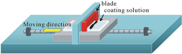
Figure 1. Blade coating operation.
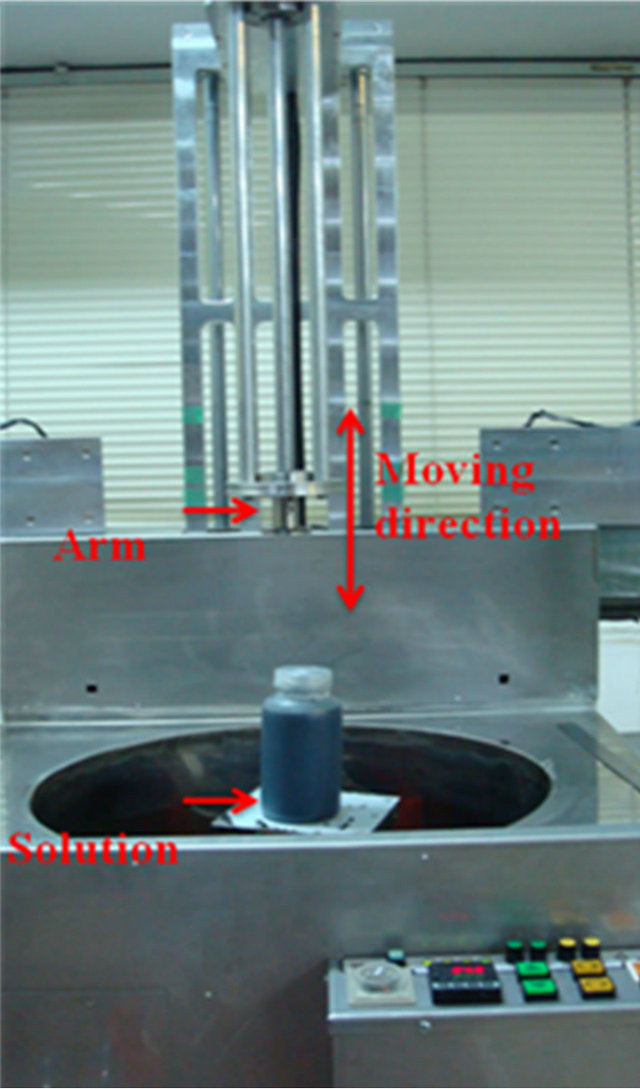
Figure 2. Photo of dip coater.
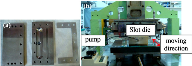
Figure 3. Photos of (a) the experimental slot die with a shim; (b) the patch coater.
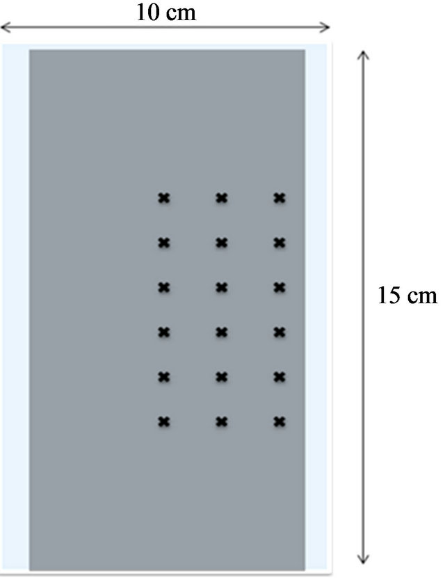
Figure 4. Sample dimensions and marked position for property measurements (10 × 15 cm2).
ples, andan UV-visible spectrophotometer (Varian Cary 50 conc) was used for transparency measurements. The uncoated PET film was used as the reference for comparison. Standard processes were taken to detect the distributions of CNT on the PET films by the scanning electronic microscope (JEOL JSM-5600).
3. Results and Discussion
The SWCNT solutions were coated on the PET substrates by the three coating methods. The transparency and sheet resistance of each coated sample were measured and analyzed.
The results obtained on slot die coating are presented first. In order to produce a very thin wet thickness on the slot die coater, the concentration of the SWCNT solutions must be reduced to 0.1%. This yielded a dry film with thickness as low as 5 nm. The dry film thickness t reported here is an average value which depends on flow rate, coating speed and solid content, t can be evaluated with the following formula:
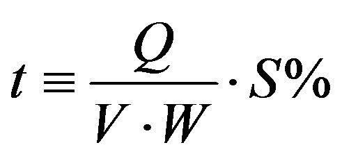 (1)
(1)
here Q is the volumetric flow rate, V is the coating speed, W is the coated width and S% is the solid content. Figure 5 presents the results of transparency and sheet resistance as a function of dry film thickness at the coating speed 10 cm/s. The results indicate that both the sheet resistance and transparency decrease as the dry film thickness increases. The increase in dry thickness is due primarily to the increasing amount of CNT accumulated on the PET substrate. Hence, it is expected that both the sheet resistance and transparency will decrease.
The effects of the coating speed on the sheet resistance and transparency for two different dry film thicknesses, 5 nm and 10 nm, are displayed in Figure 6. It is seen that both transparency and sheet resistance are independent of the coating speed for the thinner film; whereas these two
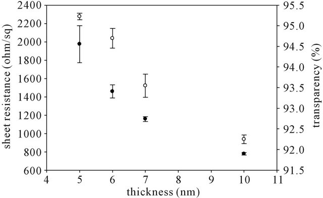
Figure 5. Sheet resistance and transparency as a function of dry film thickness for samples made by slot die coating (●: sheet resistance (ohm/sq); ○: transparency (%)).
properties decrease slightly as the coating speed increases for the thicker film. The sheet resistance stays around 2000 ohm/sq, and provides a transparency of around 95% for the 5 nm film; where the resistance drops to below 1000 ohm/sq, transparency reduces to about 92% for the 10 nm film when the coating velocity increases from 6 to 10 cm/s. At low coating speed, the coating solution emanating from the slot die exit will expand laterally, but the coating width will contract as the coating speed increases. The lateral movement of coating solution changes the CNT distribution, and affects the two properties. It is noted that the lateral expansion ceases to exist at high coating speed.
Figure 7 shows the results obtained with a blade coater having a coating gap of 20 μm. The wet film thickness for blade coating is usually less than 50% of the blade gap for dilute Newtonian solutions [22]. The average dry film thickness can be evaluated if the solid content is known, which is around 7 - 8 nm in present study. It can be seen that both the sheet resistance and transparency decrease markedly as the coating speed increases. The transparency drops from 95% to 91%, and
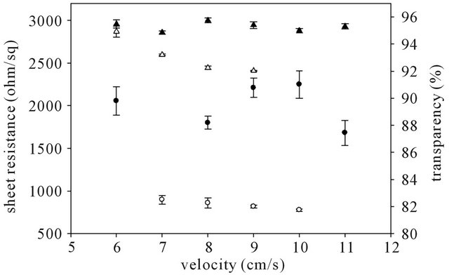
Figure 6. Sheet resistance and transparency as a function of coating speed for slot die coating (●: 5 nm (ohm/sq); ○: 10 nm (ohm/sq); ▲: 5 nm (%); △: 10 nm (%)).
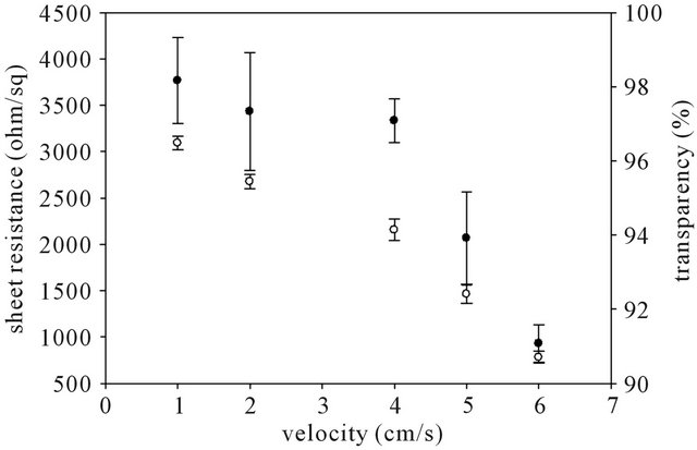
Figure 7. Sheet resistance and transparency as a function of coating speed for blade coating (●: sheet resistance (ohm/sq); ○: transparency (%)).
the resistance decreases from 3000 to below 1000 ohm/ sq when the coating speed increases from 1.0 to 6.0 cm/s. This is due to the increase of the coating thickness as the coating speed increases for a blade coater. The present observation is consistent with the conclusion of Yang and Jiang [23]. During the blade coating operation, the coating solution moves in the transverse direction as the blade advances. This lateral movement becomes more significant when the blade speed is faster.
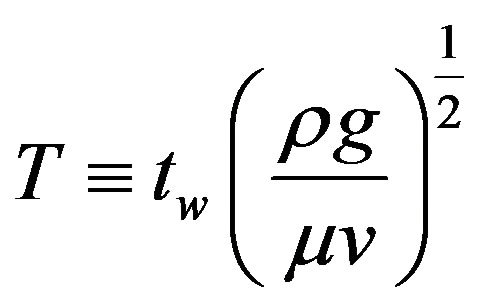
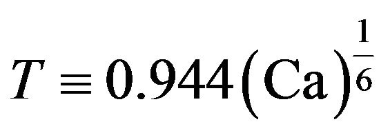
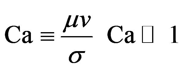
For a dip coating operation, the wet coated thickness is known to be proportional to the capillary number Ca as follows [24]:
 (2a)
(2a)
 (2b)
(2b)
here
 (2c)
(2c)
Here tw is the wet film thickness, ρ is fluid density, g is the gravitational factor, μ is the fluid viscosity and σ is the surface tension.
It was estimated the dry film thickness for dip coating is around 5 - 15 nm. Increasing the coating speed will increase Ca, and hence the coated film thickness for a coating solution of constant viscosity and surface tension. Therefore, both transparency and sheet resistance will drop in dip coating operated at higher velocity. The results obtained from dip coating are not presented here in similar plots as in Figures 6 and 7. Instead, they are combined for comparison purposes with the results of slot and blade coatings in the subsequent figures.
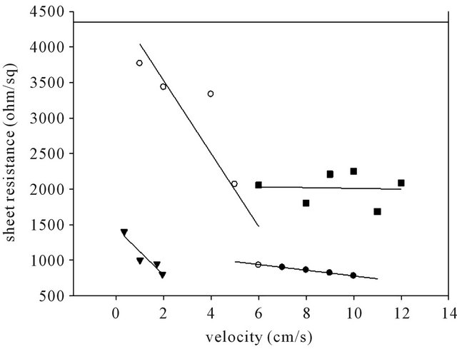
Comparison of the performance of samples based on three different coating methods is displayed in Figure 8. For dip and blade coating operations, both sheet resistance and transparency decrease with increasing coating speed. However, in order to meet the requirement of 85% transparency and sheet resistance 1000 ohm/sq, the upper limit of the coating speed for dip coating is only around 2 cm/s, and slightly above 6 cm/s for blade coating. As mentioned earlier, the optic-electronic properties appear to be independent of the coating speed in slot die coating for the 5 nm film and drop slightly for the 10 nm film when operated at a speed as high as 10 cm/s.
An attempt is made to check if a correlation exists between the sheet resistance and the transparency data obtained with the three coating methods, as shown in Figure 9. It is noted that the specific requirements of sheet resistance of around 1000 ohm/sq and transparency above 85% are satisfied for all samples obtained using the three coating methods, except for the dip coating operated at a speed of around 2 cm/s. Figure 9 reveals that
 (a)
(a)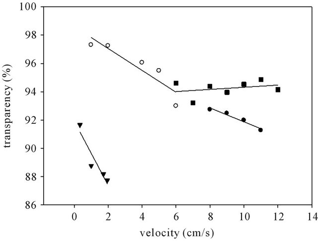 (b)
(b)
Figure 8. (a) Comparison of sheet resistance as a function of coating speed for different coating methods (■: slot 5 nm; ●: slot 10 nm; ○: blade; ▼: dip); (b) Comparison of transparency as a function of coating speed for different coating methods (■: slot 5 nm; ●: slot 10 nm; ○: blade; ▼: dip).
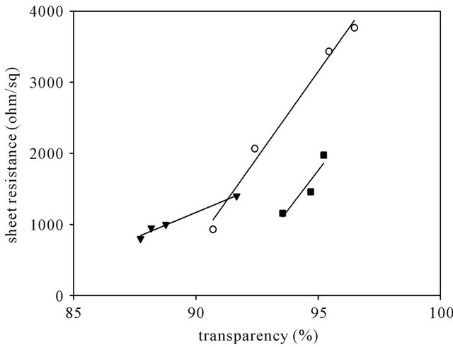
Figure 9. Sheet resistance vs. transparency for the three coating methods (■: slot 5 - 7 nm; ○: blade; ▼: dip).
there exists a linear correlation between sheet resistance and transparency. Samples with higher transparency exhibit higher sheet resistance.
The data presented in Figures 8 and 9 are based on the average value of sheet resistance and transparency. In addition, the variations of the two properties over the width of the sample are also critical to product quality. The distributions of sheet resistance for three samples are represented by the images shown in Figure 10. Figures 10(a) and (b) are two samples of different thickness obtained in slot die coating. For the thinner sample with dry film thickness of around 5 nm, the sheet resistance is quite uniform as shown in Figure 10(a). However, once the dry film thickness is increased to around 10 nm, the result in Figure 10(b) indicates that the sheet resistance at the two lateral edges increases rapidly. This implies that there are less CNT present in these regions. This is due to the lateral expansion of the coating solution after emanating from the slot die exit, which causes the concentrations of CNT towards the edges to drop sharply. The sheet resistance distribution for blade coating shown in Figure 10(c) also indicates that the distribution is not uniform due to the lateral movement of the coating solution, with high CNT concentration appearing in the central region of the sample. Therefore, to obtain a sample with uniform CNT distribution (or sheet resistance), the lateral motion has to be minimized in two-dimensional flow.
The CNT distributions on the PET films can also be observed through SEM images. The samples were taken from the central parts of the PET films. The magnifying power was selected to be 20000×. A bar of 1.0 micrometer length was given in the bottom of each figure for comparison purposes. The surfaces of the coated samples were observed. The CNT concentrations and distributions can be analyzed qualitatively. Figures 11(a) and (b) display the images obtained for two 5 nm thick dry films using the slot die coating at coating speeds of 7 cm/s and 11 cm/s, respectively. It can be seen that CNT are randomly deposited on the PET substrate, and increasing the coating speed does not cause any significant variation of the CNT distribution. The results based on blade coating are presented in Figures 11(c) and (d). Similarly, CNT are randomly distributed on the PET film, but the CNT concentration is increased substantially when the coating speed is increased from 2 cm/s to 6 cm/s as observed in Figures 11(c) and (d). This is due to the increase of the dry film thickness in blade coating at higher speed. The results based on dip coating are shown in Figures 11(e) and (f) respectively for coating speeds of 0.7 cm/s and 2 cm/s. It is seen that CNT are also randomly distributed on the PET film, but the concentrations of CNT are much higher than those obtained from the preceding two methods, and relatively unaffected by the coating
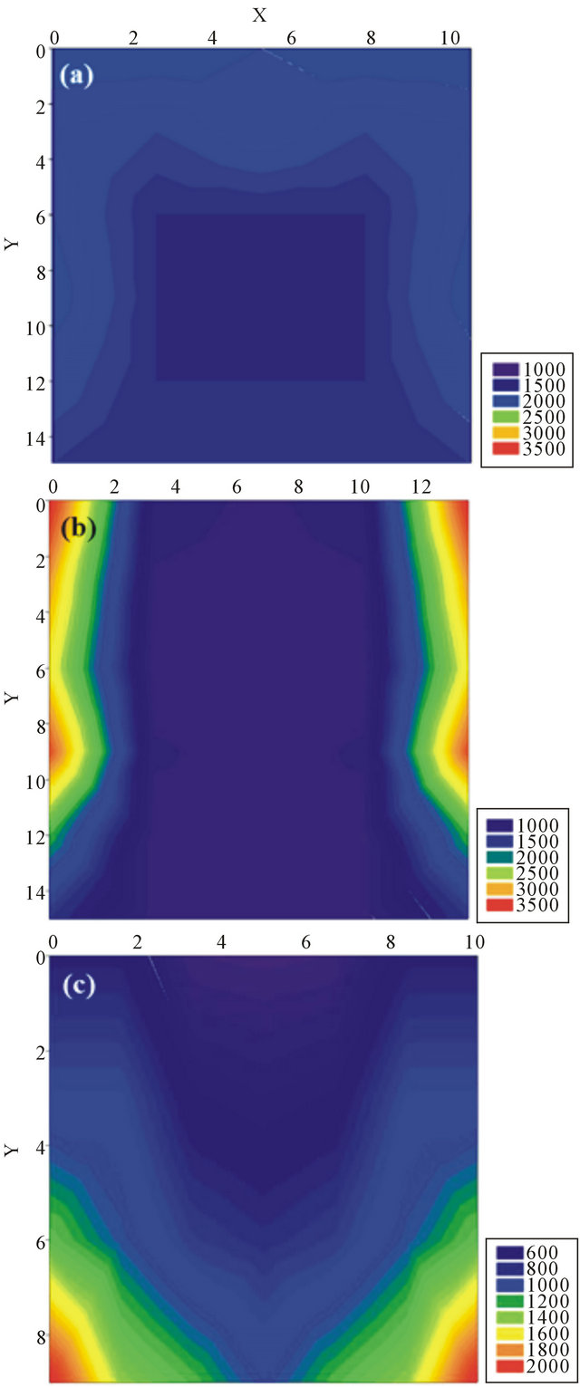
Figure 10. Images that represent sheet resistance. (a) Slot die (5 nm); (b) Slot die (10 nm); (c) Blade coating.
speed. It must be noted that the dry films obtained from dip coating are inherently thicker than those obtained from other coating methods, thus producing a higher CNT concentration on the PET surface. The cracks appeared in the SEM images certainly are not acceptable
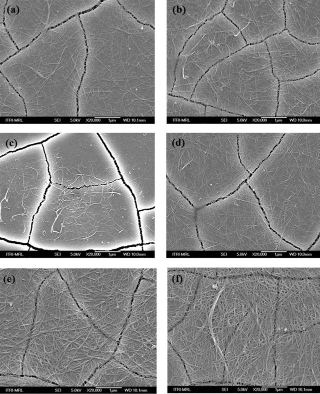
Figure 11. SEM images of samples made by the three coating methods. (a) Slot die V = 7 cm/s; (b) Slot die V = 11 cm/s; (c) Blade coating V = 2 cm/s; (d) Blade coating V = 6 cm/s; (e) Dip coating V = 0.7 cm/s; (f) Dip coating V = 2 cm/s.
for industrial applications. The present analysis focuses only on the sheet resistance and transparency of the coated CNT films. No binders, adhesives on other materials were added to the CNT solutions.
4. Conclusions
The optical-electronicproperties of PET films coated with SWCNT obtained using three different coating methods were measured and compared. The film thickness was found to increase with increasing coating speed for blade and dip coating. The film thickness for slot die coating can be controlled provided the lateral expansion of the coated film can be minimized. Higher film thickness implies high concentration of CNT, which reduces both sheet resistance and transparency of the film.
Samples produced by the three coating methods all meet the criteria of sheet resistance 1000 ohm/sq and 85% transparency at certain coating conditions. However, at coating speed higher than 8 cm/s, only the slot die coating can produce films that meet these two criteria. The SEM images reveal that CNT were randomly distributed on PET films for samples made by the three coating methods. Distributions of sheet resistance were measured for samples obtained by slot die coating and blade coating. Coating solution may expand laterally on the PET film for blade coating and slot die coating at low speeds and high flow rates. The lateral expansion of coating solution will deteriorate the uniformity of sheet resistance. By controlling the lateral movement, slot die coating can produce samples with uniform sheet resistance.
5. Acknowledgements
The research work was supported by the National Science Council under Grant No. NSC99-2221-E-007-009. MY3. K.R. Chen was supported by ITRI during this study.
REFERENCES
- T. Minami, “New n-type Transparent Conducting Oxides,” Mrs Bulletin, Vol. 25, No. 8, 2000, pp. 38-44. HHUUdoi:10.1557/mrs2000.149UU
- U. Ozgur, Y. I. Alivov, C. Liu, A. Teke, M. A. Reshchikov, S. Dogan, V. Avrutin, S. J. Cho and H. Morkoc, “A Comprehensive Review of ZnO Materials and Devices,” Journal of Applied Physics, Vol. 98, No. 4, 2005, Article ID: 041301. HHUUdoi:10.1063/1.1992666UU
- D. H. Zhang and H. L. Ma, “Scattering Mechanisms of Charge Carriers in Transparent Conducting Oxide Films,” Applied Physics A—Materials Science & Processing, Vol. 62, No. 5, 1996, pp. 487-492. HHUUdoi:10.1007/BF01567122UU
- C. C. Wang, “Deposition of Transparent Conductive Film by Wet Process,” Industrial Material Magazine, Vol. 236, 2006, pp. 173-178.
- S. Ray, R. Banerjee, N. Basu, A. K. Batabyal and A. K. Barua, “Properties of Tin Doped Indium Oxide ThinFilms Prepared by Magnetron Sputtering,” Journal of Applied Physics, Vol. 54, No. 6, 1983, pp. 3497-3501. HHUUdoi:10.1063/1.332415UU
- A. Kumar and C. W. Zhou, “The Race to Replace Tin-Doped Indium Oxide: Which Material Will Win?” ACS Nano, Vol. 4, No. 1, 2010, pp. 11-14. HHUUdoi:10.1021/nn901903bUU
- L. B. Hu, H. S. Kim, J. Y. Lee, P. Peumans and Y. Cui, “Scalable Coating and Properties of Transparent, Flexible, Silver Nanowire Electrodes,” ACS Nano, Vol. 4, No. 5, 2010, pp. 2955-2963. HHUUdoi:10.1021/nn1005232UU
- M. Kaempgen, G. S. Duesberg and S. Roth, “Transparent Carbon Nanotube Coatings,” Applied Surface Science, Vol. 252, No. 2, 2005, pp. 425-429. HHUUdoi:10.1016/j.apsusc.2005.01.020UU
- O. Hjortstam, P. Isberg, S. Söderholm and H. Dai, “Can We Achieve Ultra-Low Resistivity in Carbon NanotubeBased Metal Composites?” Applied Physics A: Materials Science & Processing, Vol. 78, No. 8, 2004, pp. 1175- 1179. HHUUdoi:10.1007/s00339-003-2424-xUU
- L. Hu, D. S. Hecht and G. Gruner, “Percolation in Transparent and Conducting Carbon Nanotube Networks,” Nano Letters, Vol. 4, No. 12, 2004, pp. 2513-2517. HHUUdoi:10.1021/nl048435yUU
- M. H. A. Ng, L.T. Hartadi, H. Tan and C. H. P. Poa, “Efficient Coating of Transparent and Conductive Carbon Nanotube Thin Films on Plastic Substrates,” Nanotechnology, Vol. 19, No. 20, 2008, pp. 205703-205707. HHUUdoi:10.1088/0957-4484/19/20/205703UU
- S. De, T. M. Higgins, P. E. Lyons, E. M. Doherty, P. N. Nirmalraj, W. J. Blau, J. J. Boland and J. N. Coleman, “Silver Nanowire Networks as Flexible, Transparent, Conducting Films: Extremely High DC to Optical Conductivity Ratios,” ACS Nano, Vol. 3, No. 1, 2009, pp. 1767-1774. HHUUdoi:10.1021/nn900348cUU
- M. C. Hersam, “Progress towards Monodisperse SingleWalled Carbon Nanotubes,” Nature Nanotechnology, Vol. 3, No. 7, 2008, pp. 387-394. HHUUdoi:10.1038/nnano.2008.135UU
- M. S. P. Shaffer and K. Koziol, “Polystyrene Grafted Multi-Walled Carbon Nanotubes,” Chemical Communications, Vol. 18, 2002, pp. 2074-2075. HHUUdoi:10.1039/b205806pUU
- C. Richard, F. Balavoine, P. Schultz, T. W. Ebbesen and C. Mioskowski, “Supramolecular Self-Assembly of Lipid Derivatives on Carbon Nanotubes,” Science, Vol. 300, No. 5620, 2003, pp. 775-778. HHUUdoi:10.1126/science.1080848UU
- T. W. Ebbesen, H. J. Lezec, H. Hiura, J. W. Bennett, H. F. Ghaemi and T. Thio, “Electrical Conductivity of Individual Carbon Nanotubes,” Nature, Vol. 382, 1996, pp. 54- 56. HHUUdoi:10.1038/382054a0UU
- S. Kim, J. Yim, X. Wang, D. D. C. Bradley, S. Lee and J. C. Demello, “Spinand Spray-Deposited Single-Walled Carbon-Nanotube Electrodes for Organic Solar Cells,” Advanced Functional Materials, Vol. 20, No. 14, 2010, pp. 2310-2316. HHUUdoi:10.1002/adfm.200902369UU
- M. J. de Andrade, M. D. Lima, V. Skakalova, C. P. Bergmann and S. Roth, “Electrical Properties of Transparent Carbon Nanotube Networks Prepared through Different Techniques,” Physica Status Solidi-Rapid Research Letters, Vol. 1, No. 5, 2007, pp. 178-180. HHUUdoi:10.1002/pssr.200701086UU
- L. J. Ci, Y. H. Li, B. Q. Wei, J. Liang, C. L. Xu and D. H. Wu, “Preparation of Carbon Nanofibers by the Floating Catalyst Method,” Carbon, Vol. 38, No. 14, 2000, pp. 1933-1937. HHUUdoi:10.1016/S0008-6223(00)00030-0UU
- J. M. Moon, K. H. An, Y. H. Lee, Y. S. Park, D. J. Bae and G. S. Park, “High-Yield Purification Process of Singlewalled Carbon Nanotubes,” The Journal of Physical Chemistry B, Vol. 105, No. 24, 2001, pp. 5677-5681. HHUUdoi:10.1021/jp0102365UU
- S. L. Kuo, S. J. Huang and C. M. Hu, “Transparent Conductive Film and Method for Manufacturing the Same,” Patent No. US20100040869-A1, 2010.
- T. M. Sullivan and S. Middleman, “Film Thickness in Blade Coating of Viscous and Viscoelastic Liquids,” Journal of Non-Newtonian Fluid Mechanics, Vol. 21, No. 1, 1986, pp. 13-38.
- H. T. Yang and P. Jiang, “Large-Scale Colloidal SelfAssembly by Doctor Blade Coating,” Langmuir, Vol. 26, No. 16, 2010, pp. 13173-13182. HHUUdoi:10.1021/la101721vUU
- L. Landau and B. Levich, “Dragging of a Liquid by a Moving Plate,” Acta Physicochimica URSS, Vol. 17, No. 42, 1942, pp. 42-54.
NOTES
*Corresponding author.