Advances in Chemical Engineering and Science
Vol. 2 No. 2 (2012) , Article ID: 18914 , 8 pages DOI:10.4236/aces.2012.22034
Synthesis and Characterization of GaN Rods Prepared by Ammono-Chemical Vapor Deposition
1Departamento de Química, Universidad de Guadalajara, Guadalajara, México
2Centro de Nanociencias y Nanotecnología, Universidad Nacional Autónoma de México, Ensenada, México
3Instituto Potosino de Investigación Científica y Tecnológica (IPICYT), División de Materiales Avanzados (LINAN), San Luis Potosí, México
4Centro de Investigación en Física, Universidad de Sonora, Hermosillo, México
Email: *gregoriocarbajal@yahoo.com.mx
Received January 17, 2012; revised February 21, 2012; accepted March 25, 2012
Keywords: Crystal morphology; Nanostructures; Chemical vapor deposition processes; Semiconducting III-V material
ABSTRACT
GaN rods were deposited by chemical vapor deposition (CVD) onto sapphire (0 0 0 1) and amorphous quartz. The reactive Ga species in vapor the phase was formed with NH4Cl and gallium. The unidirectional growth was catalyzed with gold nanoparticles formed onto the substrate prior to the CVD reaction in order to induce a vapor-liquid-solid (VLS) mechanism. However, this method of synthesis seems to be influenced by other growth mechanisms which formed additional depositions of GaN with different morphology than the rods catalyzed by gold nanoparticles. The moieties of GaN that grew in the absence of gold formed branches in the rods or increased the lateral growth of rods resulting in larger diameters than the size of the gold particle that guided the growth.
1. Introduction
Gallium nitride is an attractive semiconductor since its 3.4 eV gap band is suitable for use in optical devices and integrated circuits that operate in wavelengths of the blue-violet and ultra-violet regions [1]. Chemical vapor deposition (CVD) is one of the most investigated methods of GaN synthesis involving different types of gallium-containing reagents that form reactive gallium species in the vapor phase. However, this technique has countless factors that must be controlled such as the type of precursors, concentrations, substrate composition, deposition temperature, and the nature of the catalysts to produce a desired morphology. For instance, in the simplest CVD setup to prepare GaN from only metallic gallium and ammonia, the changes in reagent concentration lead to formation of amorphous GaN, pellets or rods [2].
By increasing the number of reagents, the system becomes more complex, although the use of more reagents may be justified if the reactivity of gallium precursors increases, thus affording a lower reaction temperature or if the reagents are less toxic. This is the case of a method to produce bulk GaN under high pressures with an ammonium halide salt (NH4X, where X = Cl, Br, or I) that sublimes and forms a gallium complex with metallic gallium, and then the complex reacts with NH3 to form GaN [3]. These reagents, which are inexpensive and easy to handle, have been used in a CVD system resulting in formation of GaN-containing columns [4]. However, the use of NH4Cl leads to a series of additional reactions that increase lateral growth with only a change of the reaction temperature [5].
On the other hand, a key point to grow GaN rods, i.e., to favor a larger L/D aspect ratio (length to diameter) to that of columns, is a metal catalyst, or foreign element catalytic agent (FECA) [6], which is used as a metal cluster or nanoparticle. The growth mechanism of GaN wires with metal catalysts has been described by Lieber [7,8] and is based on the capacity of the metal to dissolve gallium and nitrogen under the reaction conditions, as would happen with metallic iron or nickel at 900˚C [8] or 650˚C [9], respectively. This reaction is called the vapor-liquid-solid (VLS) mechanism [10], since gallium and nitrogen are transferred from the vapor (V) phase to the liquid (L) metal cluster phase and then solidify (S) as GaN, retaining the catalytic droplet on the tips of the rods as the special feature of this process.
In this particular metal cluster catalysis, if one element which is to form the rod is not soluble in the metal catalyst, as in the similar case of nitrogen in gold [8,11] for example, the nanorods are not formed, as confirmed earlier by Duan et al. [7]. Nonetheless, recent experiments have demonstrated the formation of GaN nanowires employing gold clusters as catalyst when triethyl gallium and ammonia were used as the reagents [8,11].
Our objective in this investigation is to prepare gold clusters in situ through the annealing of a thin film deposited on sapphire (0 0 0 1) substrate and amorphous quartz and determine whether this substrate influences the formation of clusters. Then, we intend to characterize the rods grown with this practical method in order to know their properties and propose suitable applications.
2. Materials and Methods
2.1. Chemical Vapor Deposition (CVD)
Reagents used in this work were metallic gallium (Sigma Aldrich, USA, 99.9995%), ammonium chloride (Fagalab, Mexico, 99.5%), and ammonia gas (Praxair, México, 99.99%). Sapphire (0 0 0 1) and amorphous quartz substrates areas of 1 - 1.5 cm2 were cleaned with acetone in an ultrasound bath, dried in air, and then transferred to a vacuum chamber (JEOL-JEE-400) where a gold film of ~10 nm in thickness was deposited by vacuum sputtering onto the surfaces of the substrates. The CVD system was assembled in a Lindberg-Blue horizontal furnace Model STF55433C with a 2-inch diameter quartz tube. All reactions were conducted at atmospheric pressure. A boat with 3.0 g of NH4Cl was placed at the entrance of the furnace. The temperature at this position was maintained at 350˚C, which is sufficient to sublime NH4Cl and to promote the formation of a gaseous gallium chloride precursor [3,4,12,13]. A quartz crucible with 0.7 g of gallium was placed 10 cm downstream from the position of the ammonium salt and the sapphire substrate with the gold film, separated by 1.0 cm from the crucible with the gallium metal source. Unlike other reports, where the gold film has been annealed prior to the GaN synthesis to assure the presence of gold nanoparticles, in the experiment described herein , the substrate with the gold film was placed in the CVD reactor without annealing.
A schematic representation of this setup is shown elsewhere [4,14]. The furnace was heated at a rate of 30˚C·min−1 and maintained at 800˚C. The tube was purged with ammonia when the temperature in the furnace was 300˚C and the flow rate was constant at 180 sccm until the end of the reaction. Then, the system was cooled to room temperature by switching off the heater. The exhaust gases were collected in an aqueous HCl solution trap.
2.2. Characterization
Electron scanning microscopy images were collected with a JEOL JSM5300 system and a cathode luminescence (CL) system using an electron beam with an energy of 15 keV. The structures were analyzed with a Phillips X’pert-MDP diffractometer with Cu kα radiation (0.15404 nm). Nanoparticle dimensions were estimated by analyzing SEM images with Image Tool v 3.0 [15]. TEM images were collected with a JEOL 2010 microscope and a FEI model TECNAI F-30 operated at 300 keV adapted with an EDS detector. Atomic Force Microscopy (AFM) images were acquired with a Nanoscope III system.
3. Results and Discussion
3.1. SEM
The first step in the synthesis of GaN rods is the deposition of gold clusters onto the substrate surface. Instead of separately annealing the gold film prior to CVD synthesis [4], we prepared the gold clusters in situ by introducing the substrate with the gold film directly into the CVD reactor along with the reagents required for GaN deposition. This is the actual environment in which gold clusters promote the growth of GaN. This in situ annealing seemed feasible since the minimal temperature to form the clusters is 200˚C, independent of time, which can range from 1 to 30 minutes [16]. Thus, by applying a heating rate of 30˚C·min−1, there is sufficient temperature and time (ca. 26 min) to form the clusters before reaching the operational temperature of 800˚C for this reaction. A similar in situ annealing was successful when gold was deposited onto a silicon substrate [17]. Sapphire and quartz were used to verify influences of substrate crystallinity on either the formation of gold clusters or the growth of GaN.
GaN deposition only starts when the temperature in the furnace is 800˚C, since this corresponds to 350˚C at the entrance of the furnace where the NH4Cl sublimes and transfer the metal gallium to the vapor phase [4,18].
In two experiments, the substrates were removed at this step to analyze the clusters by XRD and SEM (Figures 1(a), (b)). The depositions carried out with quartz and sapphire substrates were identified by XRD as GaN with a hexagonal wurtzite-type structure (patterns not shown herein), matching with the JCPDS card 74-0243 [19]. The GaN deposited onto quartz exhibited relative intensities similar to that of the powder pattern of the card, whereas the sample grown onto sapphire showed greater intensity for the [002] reflection, as a consequence of the preferential orientation of the rods in rela-
 (a)
(a)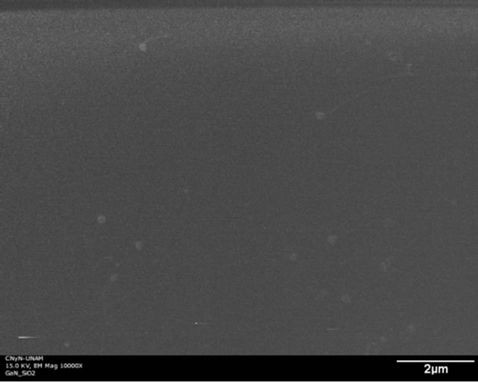 (b)
(b)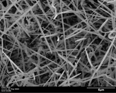 (c)
(c)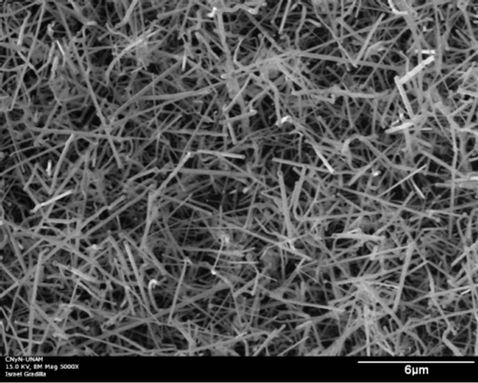 (d)
(d)
Figure 1. SEM images of gold clusters formed onto (a) sapphire and (b) quartz; and the rods grown with these clusters in (c) sapphire and (d) quartz.
tion to the substrate.
Other substrates with gold films were treated with the same procedure and allowed to react 30 minutes at 800˚C to obtain GaN rods (Figures 1(c) and (d)). The images were analyzed with an image program to determine particle dimensions [15].
It should be noted that due to the NH3 atmosphere (applied when the furnace reached 300˚C) and the reagents in the CVD reactor, traces of gallium, nitrogen or chloride could be present in the cluster. Henceforth, the clusters formed before the start of NH4Cl sublimation will be called “clusters”, while the particles which remained on the tips of GaN rods will be named “droplets” because they form liquid droplets during the growth of the GaN rods [6-8,10].
Figure 2 shows the AFM image of gold clusters formed by annealing the gold film on sapphire. The sizes are ~250 nm, close to the results obtained from the analysis of SEM images.
Table 1 gives the mean dimensions of the clusters, rods, and droplets on the tips to indicate the relationship between these particles. The dimensions of initial gold clusters are essentially the same as the rods diameters on quartz (170 vs. 150 nm) and on sapphire (215 vs. 225 nm). These data suggest that the size of the pristine gold clusters (i.e., before GaN growth) may determine the diameter of the rods. Table 1 also shows that pristine clusters (before GaN growth) are slightly smaller than the droplets on the tip of the rods on quartz (170 vs. 210 nm) and sapphire (215 vs. 270 nm). This observation may be explained by swelling in the vapor-liquid (V-L) phase, where the gallium is dissolved by gold, thereby
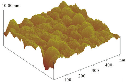
Figure 2. AFM image of the gold particles formed on sapphire during the heating ramp of the CVD system.
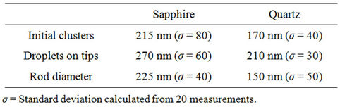
Table 1. Relationship between sizes of gold clusters, droplets on the rod tips and rods.
increasing the droplet size. Incorporation of nitrogen is discarded because of its negligible solubility in gold at the reaction temperature [8,11].
To confirm the swelling of the cluster, commercial gold nanoparticles of ~50 nm in diameter were dropped onto sapphire and quartz substrates. These samples were then analyzed by SEM with back-scattered electrons to highlight the gold droplets (Figures 3(a) and (b)). The size of droplets without GaN formation is that of rod width (Figure 3(a)), suggesting that in the earlier stage of growth, the width depends on the cluster size. This confirms that the amount of gallium being dissolved by the droplet is transferred to the L-S interface. However, gallium diffusion through the droplet is slow and due to this, gallium concentrates itself, resulting in an increase in the size of the droplet. As a result, bigger droplet size is found particularly in large rods.
The presence of the droplet on the tip indicates that they may be responsible for the unidirectional growth of GaN. In principle, this observation could be associated with a vapor-liquid-solid (VLS) mechanism, as other authors have mentioned [8] and that the mechanism could be inferred from the morphology and size of the droplet as well as its relationship with the diameter of the rod [6]. This discussion is addressed in the next section.
3.2. TEM: Effects of Nitrogen Insolubility in the Droplet
TEM images of rods grown onto quartz and sapphire
 (a)
(a) (b)
(b)
Figure 3. SEM images with back-scattered electrons of GaN rods and gold droplets onto (a) quartz and (b) sapphire.
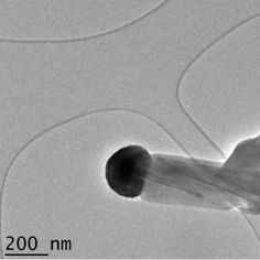
showed well-faceted droplets on the tips, which were also larger than the rod diameters. Figures 4(a) and 6(a) are examples of rods and droplets with these features which represent the majority of specimens observed. Nonetheless, isolated cases of quasi-spherical droplets were also found (Figures 4(b) and 6(b)).
A droplet in liquid state would be spherical, but when the temperature of the CVD system decreased the droplet crystallized with defined faces [8]. It is possible that the droplets were not only formed by gold because, as reaction centers for GaN growth, they should contain at least gallium or GaN. The spectra collected with the EDS detector of the TEM microscope show the profile of gallium and gold content along the length of a rod to the tip with the droplet (Figure 5). The intensity of the gallium spectrum decreased in the position from 0.5 to 0.15 μm, which could be a result of a gallium-deficient zone, as reflected in the cathode-luminescence spectrum that will be shown later. Then, when the electron beam reached the droplet (at 0.20 μm), the intensity for gold increased, whereas the signal for gallium decreased but did not disappear, confirming that the droplet is formed by a mixture of gold and gallium.
Although the presence of droplets on the rods is an indication that the growth followed the VLS mechanism [9], some variations could be involved. Since the elements forming the rods have to be dissolved by the metal catalyst [8], and nitrogen is not miscible in gold at 900˚C [8,11], the prediction indicates that GaN rods could not be grown by this method. However, the gold-catalyst did produce rods in the ammono-CVD system. In order to discount any possible unidirectional growth of GaN induced by the crystalline sapphire or the amorphous quartz, additional experiments performed in the absence of gold produced only continuous polycrystalline films [5], suggesting that the gold particles can act as a catalyst to form GaN rods under these experimental conditions.
The insolubility of nitrogen in the droplet seems to be unimportant for rod formation since the continuous flow of ammonia guarantees constant contact of nitrogen with the surface of the droplet containing gallium.
Thus, the contact of gaseous nitrogen with the liquid gold-gallium droplet seems to be sufficient to form GaN
 (a)
(a) (b)
(b)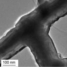 (c)
(c) (d)
(d)
Figure 4. TEM images of GaN rods grown onto quartz.
Figure 5. Gallium and gold content profile detected by EDS along the rod.
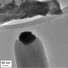
with a unidirectional structure as proposed by Gottschalch et al. [11]. Thus, the actual mechanism is probably related to a VLS mechanism with regards to gallium. Finally, the lack of nitrogen solubility in the droplet may account for the large number of crystalline faults along the rods, the irregular diameters, and the rough surfaces observed in these samples (Figures 4(a)-(d) and 6(a)- (c)).
3.3. TEM: Effects of Gallium Diffusion through the Droplet and Gallium Concentration in the Gas Phase
The diffusion capacity of gallium through gold influences the morphology of the droplet (shape and size) and the rod [6].
The observations made by Mohammad [6] on rods with different compositions led to the conclusion that metal droplets are larger than the rod diameters because
 (a)
(a)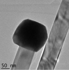 (b)
(b)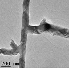 (c)
(c)
Figure 6. TEM images of GaN rods grown onto sapphire.
of low diffusion of the atoms that form the rod through the droplet in the liquid state. In our experiments, the droplets were clearly larger than the diameters of the rods, but in addition the droplets were well-faceted (Figures 4(a), (c) and 6(a)). If gallium diffuses at a slow rate through gold, it is expected that the droplet accumulates gallium and swells, and that larger droplets are then found at the end of the reaction in comparison to the size of the gold particles which are obtained by simple annealing, as shown in Figure 2.
Another consequence of low diffusion of gallium could be poor transfer of gallium to the L-S interface, which could result in the formation of thin rods. On the contrary, the accumulation of gallium in the droplet could be responsible for the faceted morphology of the droplet, since gold nanoparticles of 200 nm tend to be spherical.
The widening of rods is inherent to this CVD system [5] and occurs in addition to the gold catalyzed growth. The surfaces of the GaN rods formed are continuously exposed to gallium and nitrogen reagents in the vapor phase in such a way that the vapor reagents could react on the rod surface. One fact in accordance with this is found in the TEM images of rods onto quartz and sapphire. The size of droplets in Figures 4(a) and 6(a) are near to 100 nm, while the rods are thinner. However, even when the droplets in Figures 4(b) and 6(b) are still near to 100 nm, the width of the rods increased to 220 nm (Figure 4(b)) or to 100 nm (Figure 6(b)). This widening could not be related to the presence of gold but to the further reaction of the reagents in the vapor phase.
Another evidence of the extra widening was detected in the rods grown onto quartz. In this deposition there was a darker area visible at naked eye corresponding to the zone of the substrate exposed directly to the gallium boat. The SEM image of this region shows columnar structures (Figure 7) suggesting that the diameter increased by the side deposition of GaN, influenced by the exposition to a higher concentration of gallium reactive species.
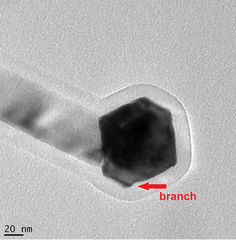
3.4. TEM: Branches in GaN Rods
Another observation is that the rods formed branches with a diameter similar to or smaller than that of the main rods (Figures 4(d) and 6(c)). The orientations of branches did not follow a regular trend; they grew at angles ranging from 83 to 157 degrees, including T shaped branching.
The formation of these branches may be explained as secondary growth originating from the convergence of an L-S interface with the nitrogen present around the droplet in the V phase (Figure 8), which may react to form GaN by a V-S step.
As a result of the accumulation of gallium in the gold droplet (as discussed earlier), the possibilities to react with nitrogen increase, but solidification of GaN requires a L-S interface, which can be found close to the rod (dashed area in Figure 8). Evidences of incipient branching were found in samples of both substrates (Figures 9(a), (b)). The further growth of the branch cannot be associated with a gold catalyzed pathway because we did not find any droplet division. It was rather seen that the droplet either deviates and catalyzes the formation of a branch (Figure 6(c)), or follows the main rod to form a side branch (Figure 6(c)) according to the model de-

Figure 7. SEM image of the quartz zone exposed directly to the gallium stream.
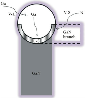
Figure 8. Scheme of GaN nucleation in the L-S interface.
 (a)
(a)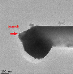 (b)
(b)
Figure 9. TEM images of GaN rods with incipient branching in samples grown onto (a) sapphire and (b) quartz.
picted in Figure 8. Thus, the rod without the presence of a droplet should continue to grow by replicating the structure of crystalline GaN without the need for a catalyst.
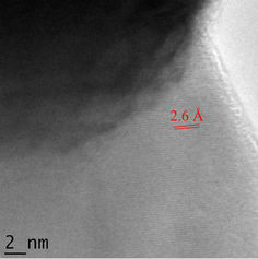
3.5. HRTEM
The GaN rods contained a large amount of crystalline faults, as expected, since the gold droplet did not form a complete solution with nitrogen. Despite the faults and the large thickness of the rods, HRTEM images were collected which revealed that the rods grew along the c axis (Figure 10). Thus, the droplet is supported by the (0002) plane of GaN which has an interplanar spacing of 2.6 Å.
3.6. Cathodoluminescence
The CL spectra collected at room temperature (Figure 11) reveals a broad band-edge emission at 380 nm (3.26 eV) commonly associated with GaN with a wurtzite-like structure. Typical emission of the near band edge in GaN structures has been detected at 365 - 378 nm [20-22],
 (a)
(a) (b)
(b)
Figure 10. HRTEM images of GaN rod grown on (a) quartz and (b) sapphire.
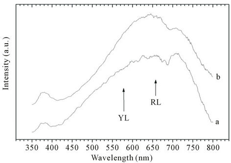
Figure 11. Room-temperature CL spectra of GaN deposited on (a) sapphire and (b) quartz.
which is the donor bound exciton emission [20]. This band can be broad [23] due to donor acceptor pair in GaN nanowires [20].
In addition, a broad and high intensity band emission above 500 nm was observed and assigned to defect-rich crystallites [24,25]. The broad band is composed of yellow luminescence (YL) and red luminescence (RL). The former is caused by gallium vacancies while the red luminescence is produced in regions with nitrogen deficiency [22]. Both of these regions are exhibited by the GaN rods obtained on sapphire and quartz, indicating that the formation of defects depends on the type of reagents used in the ammono-CVD system and not on the substrate.
The RL intensity was even higher than the YL, thus indicating several sites in the GaN structure with nitrogen deficiency. This fact has coherency with the hypothesis stating that nitrogen is poorly soluble in the gold droplet, i.e. the lower possibility of nitrogen to reach the L-S interface, in comparison with gallium, produces nitrogen deficient sites. The presence of crystalline defects makes GaN prone to react with some chemical species like gases or even with more complex molecules like amino acids as some preliminary experiments proved, and such surface reactions induce changes in electrical conductivity. This behavior can be useful to design chemical sensors. Additionally, the 1D structures obtained in this work provide a larger contact area in comparison with films.
4. Conclusions
Formation of gold clusters in situ is feasible during the heating ramp of the CVD system with a heating rate of 30˚C·min−1 up to 800˚C. Gold particles formed onto amorphous or crystalline surfaces like quartz and sapphire substrates are effective in catalyzing the growth of GaN rods. The diameter of the rods depends on the size of the gold particles, without the influence of the sapphire or quartz substrate surface once the growth of crystalline GaN had been initiated.
GaN rods grow by a VLS mechanism even when only gallium is dissolved by the droplet, by reaction in the V-S region with nitrogen. Since nitrogen surrounds the gallium/gold droplet surface, the region near the L-S interface could form branches; when this occurred, the droplet is not divided and guides either the main rod or a branch. The rods undergo lateral growth, influenced by the gallium complex in the vapor phase. Gallium has a low rate of diffusion through the gold droplet, resulting in the accumulation of gallium, thereby increasing the volume of the droplet. After cooling, well-faceted droplets formed on the tips. The GaN on both substrates possessed a wurtzite-like structure according to the X-ray analysis and CL spectra.
Owing to the insolubility of nitrogen in the droplet, rods exhibit crystalline defects, reflected in the wide red band of the CL spectra, despite this, the crystalline defects represent an opportunity to develop devices for gas sensing since this sites are prone to react with foreign chemical compounds changing the electrical conductivity. The use of NH4Cl to transfer gallium to the vapor phase is a good alternative to prepare GaN in a CVD system, being possible to grow rods with gold as catalyst.
5. Acknowledgements
We are grateful to the technical assistance of I. Gradilla, E. Aparicio, F. Ruiz, E. Flores, J.A. Diaz Hernandez, D. Dominguez and M.I. Perez Montfort. Financial support was provided by DGAPA-UNAM (project IN109612) and CONACYT (project 82984). We also thank M. Avalos Borja for helpful suggestions and for providing access to LINAN’s electron microscopy facilities.
REFERENCES
- E. Estephan, et al., “Tailoring GaN Semiconductor Surfaces with Biomolecules,” Journal of Physical Chemistry B, Vol. 112, No. 29, 2008, pp. 8799-8805. doi:10.1021/jp804112y
- M. He, et al., “Growth of GaN Nanowires by Direct Reaction of Ga with NH3,” Journal of Crystal Growth, Vol. 231, No. 3, 2001, pp. 357-365. doi:10.1016/S0022-0248(01)01466-X
- D. Ehrentraut, et al., “Physico-Chemical Features of the Acid Ammonothermal Growth of GaN,” Journal of Crystal Growth, Vol. 310, No. 5, 2008, pp. 891-895. doi:10.1016/j.jcrysgro.2007.11.090
- R. Garcia, A. C. Thomas and F. Ponce, “Measurement of the Solubility of Ammonia and Nitrogen in Gallium at Atmospheric Pressure,” Journal of Crystal Growth, Vol. 467, No. 1-2, 2008, pp. 3131-3134. doi:10.1016/j.jcrysgro.2008.03.030
- G. G. C. Arízaga, et al., “Influence of Reaction Conditions on the Growth of GaN Rods in an Ammono-CVD Reactor,” Journal of Crystal Growth, Vol. 319, No. 1, 2011, pp. 19-24. doi:10.1016/j.jcrysgro.2011.01.103
- S. N. Mohammad, “Why Droplet Dimension Can Be Larger than, Equal to, or Smaller than the Nanowire Dimension,” Journal of Applied Physics, Vol. 106, 2009, Article ID: 104311, pp. 1-11.
- A. Morales and C. M. Lieber, “A Laser Ablation Method for the Synthesis of Crystalline Semiconductor Nanowires,” Science, Vol. 279, No. 5348, 1998, pp. 208-211. doi:10.1126/science.279.5348.208
- X. Duan and C. M. Lieber, “Laser-Assisted Catalytic Growth of Single Crystal GaN Nanowires,” Journal of the American Chemical Society, Vol. 122, No. 1, 2000, pp. 188-189. doi:10.1021/ja993713u
- L. Yu, Y. Ma and Z. Hu, “Low-Temperature CVD Synthesis Route to GaN Nanowires on Silicon Substrate,” Journal of Crystal Growth, Vol. 310, No. 24, 2008, pp. 5237-5240. doi:10.1016/j.jcrysgro.2008.09.191
- R. S. Wagner and W. C. Ellis, “Vapor-Liquid-Solid Mechanism of Single Crystal Growth,” Applied Physics Letters, Vol. 4, No. 89, 1964, pp. 89-90. doi:10.1063/1.1753975
- V. Gottschalch, et al., “VLS Growth of GaN Nanowires on Various Substrates,” Journal of Crystal Growth, Vol. 310, No. 23, 2008, pp. 5123-5128. doi:10.1016/j.jcrysgro.2008.08.013
- P. Purdy, “Ammonothermal Synthesis of Cubic Gallium Nitride,” Chemistry of Materials, Vol. 11, No. 7, 1999, pp. 1648-1651. doi:10.1021/cm9901111
- T. Hashimoto, et al., “Growth of Gallium Nitride via Fluid Transport in Supercritical Ammonia,” Journal of Crystal Growth, Vol. 275, No. 1-2, 2005, pp. e525-e530. doi:10.1016/j.jcrysgro.2004.11.024
- G. G. C. Arizaga, et al., “Reversible Intercalation of Ammonia Molecules into a Layered Double Hydroxide Structure without Exchanging Nitrate Counter-Ions,” Journal of Solid State Chemistry, Vol. 183, No. 10, 2010, pp. 2324-2328. doi:10.1016/j.jssc.2010.07.050
- Image Tool Version 3.0. http://ddsdx.uthscsa.edu/dig/itdesc.html
- Ch. Y. Chang, et al., “Control of Nucleation Site Density of GaN Nanowires,” Applied Surface Science, Vol. 253, No. 6, 2007, pp. 3196-3200. doi:10.1016/j.apsusc.2006.07.007
- Ch. Cao, X. Xiang and H. Zhu, “High-Density, Uniform Gallium Nitride Nanorods Grown on Au-Coated Silicon Substrate,” Journal of Crystal Growth, Vol. 273, No. 3-4, 2005, pp. 375-380. doi:10.1016/j.jcrysgro.2004.09.050
- S. E. Alexandrov, A. Y. Kovalginy and D. M. Krasovitskiy, “A Study of CVD of Gallium Nitride Films by In-Situ Gas-Phase UV Spectroscopy,” Journal de Physique IV, Vol. 5, No. C5, 1995, pp. 183-190. doi:10.1051/jphyscol:1995520
- Data Collection of the Joint Committee on Powder Diffraction Standard, PCPDFWIN Version 2.2, June 2001.
- Y. H. Ra, et al., “The Influence of the Working Pressure on the Synthesis of GaN Nanowires by Using MOCVD,” Journal of Crystal Growth, Vol. 312, No. 6, 2010, pp. 770-774. doi:10.1016/j.jcrysgro.2009.12.056
- R. Navamathavan, et al., “Different Growth Behaviors of GaN Nanowires Grown with Au Catalyst and Au + Ga Solid Solution Nano-Droplets on Si(111) Substrates by Using MOCVD,” Current Applied Physics, Vol. 11, No. 1, 2011, pp. 77-81. doi:10.1016/j.cap.2010.06.022
- D. S. Chander, J. Ramkumar and S. Dhamodaran, “Controlled 1-D to 3-D Growth Mode Transition of GaN Nanostructures and Their Optical Properties,” Physica E, Vol. 4. No. 9, 2011, pp. 1683-1687. doi:10.1016/j.physe.2011.05.022
- Y. H. Cho, et al., “Optical Properties of Laterally Overgrown GaN Pyramids Grown on (111) Silicon Substrate,” Current Applied Physics, Vol. 2, No. 6, 2002, pp. 515- 519. doi:10.1016/S1567-1739(02)00168-2
- S. Q. Zhou, et al., “Comparison of the Properties of GaN Grown on Complex Si-Based Structures,” Applied Physics Letters, Vol. 86, No. 8, 2005, pp. 1-3. doi:10.1063/1.1868870
- A. N. Red’kin, et al., “Chemical Vapor Deposition of GaN from Gallium and Ammonium Chloride,” Inorganic Materials, Vol. 40, No. 10, 2004, pp. 1049-1053. doi:10.1023/B:INMA.0000046466.62619.e9
NOTES
*Corresponding author.