Advances in Materials Physics and Chemistry
Vol.3 No.2(2013), Article ID:33324,6 pages DOI:10.4236/ampc.2013.32026
Effect of Side Chain of Oligothiophene Derivatives on Bulk Heterojunction Structure in Organic Photovoltaic Devices
1National Institute of Advanced Industrial Science and Technology (AIST), Ibaraki, Japan
2Graduate School of Engineering, Kobe University, Hyogo, Japan
3Interdisciplinary Graduate School of Science and Engineering, Tokyo Institute of Technology, Kanagawa, Japan
Email: 081t904t@stu.kobe-u.ac.jp
Copyright © 2013 Kenichi Sasaki et al. This is an open access article distributed under the Creative Commons Attribution License, which permits unrestricted use, distribution, and reproduction in any medium, provided the original work is properly cited.
Received February 25, 2013; revised May 1, 2013; accepted May 16, 2013
Keywords: Organic Photovoltaic Cells; Sexthiophene; Bulk Heterojunction; Morphology
ABSTRACT
The effect of the molecular structure on photovoltaic performance was investigated by comparing two types of active layers. One is an active layer formed by sexithiophene (6T) and C60 molecules which don’t have side chains. Another one is an active layer formed by a,ω-bis(2-hexyldecyl)sexithiophene (BHD6T) and [6,6]-phenyl-C61-butyric acid methyl ester (PCBM) molecules which have side chains. The 6T:C60 active layer exhibited an excessive crystallization of 6T, which led to the low photovoltaic performance. In the BHD6T:PCBM active layer, the crystallization of BHD6T was suppressed. The crystallization of BHD6T was also easily controlled by thermal annealing, which led to improved photovoltaic performance.
1. Introduction
Organic photovoltaic devices are attractive for the realization of a low cost, lightweight, flexible, large-area, and eco-friendly energy source. In recent years, a large number of high-performance organic photovoltaic devices have been reported [1-5]. In addition, fabrication techniques for printable organic photovoltaic devices have developed rapidly [6-20]. Most devices have a bulk heterojunction (BHJ) structure, which is prepared from a mixed solution containing p-type and n-type molecules. These molecules generally have side chains for the improved solubility. [6,6]-phenyl-C61-butyric acid methyl ester (PCBM) has been widely used as an n-type fullerene derivative [21]. In most cases, polymer materials have been used as a p-type derivative. In particular, poly (3-hexylthiophene) (P3HT) has high photovoltaic performance as a result of aggregation and high crystallinity [22]. Recently, some researchers have focused on soluble small molecules as p-type materials because of their higher durability and higher crystallinity [23]. Here, we investigated soluble oligothiophene based p-type semiconducting materials. Oligothiophene derivatives have been used for thin-film transistors, and the relationship between the alkyl side chain and carrier mobility has been studied [24-29]. However, there are few reports on the photovoltaic application of these oligothiophenes. To obtain high photovoltaic performance, the important factors are not only high carrier mobility but also the optimized morphology of the BHJ. It is well known that the morphology of a BHJ is affected by its molecular structure. In this study, we compared two types of active layer to investigate the effect of the alkyl side chain on the morphology and photovoltaic performance. One is an active layer formed by sexithiophene (6T) and C60 molecules which do not have side chains, as shown Figure 1(a) [30]. The other is an active layer formed by PCBM and a,ω-bis(2-hexyldecyl)sexithiophene (BHD6T) which have side chains, as shown in Figure 1(b). BHD 6T is a molecule with a complex side alkyl chain and is based on a-alkyl sexithiophene. It has high charge mobility. The material has been used as an active layer of organic thin film transistors and has a charge mobility of 0.18 cm2/Vs [31]. PCBM is an n-type soluble molecule based on fullerene and has a side chain. In addition, we investigated the effect of thermal annealing on BHD6T: PCBM devices. From our results, we clarified the effect of the molecular structure on organic photovoltaic devices.
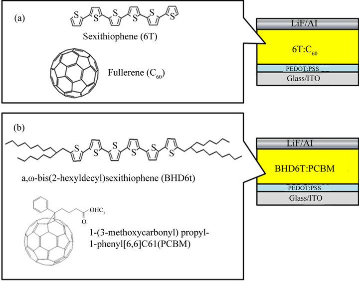
Figure 1. Device structure and molecular structure: (a) 6T:C60 device; (b) BHD6T:PCBM device.
2. Experimental
2.1. Preparation
We fabricated organic photovoltaic devices with two structures: 1) glass/ITO/PEDOT:PSS/6T:C60 (1:1)/LiF/Al; and 2) glass/ITO/PEDOT:PSS/BHD6T:PCBM (1:1)/LiF/ Al. The preparation procedure is as follows. An ITOcoated glass substrate was cleaned by ultrasonication in acetone, an alkaline detergent, water and an ethanol solvent successively, then was exposed to ozone. Poly(3,4- ethylenedio-xylenethiophene):polystyrene sulphuric acid (PEDOT:PSS) was spin-coated on the substrate. The active layer of 6T:C60 was prepared by vacuum co-deposition. The deposition rates of 6T and C60 were 0.015 nm/s. The active layer of BHD6T:PCBM was prepared by spin-coating from a chloroform solution containing BHD6T (1 wt%) and PCBM (1 wt%). Then, the substrate was annealed on a hot plate inside a glove box filled with nitrogen. After the formation of the active layer, a LiF (2 nm) and Al (100 nm) electrode were deposited in a vacuum of 10−5 Pa.
2.2. Measurement
The photovoltaic characteristics were measured using a source meter (Keithley 2400, Keithley Instruments Inc.) under a light-illuminated condition. The light source was a solar simulator (OTENTO-SUN III, Bunkoukeiki Co., Ltd.), whose light was adjusted to air mass (AM) 1.5 G, 100 mW/cm2. Differential thermal analysis (DTA) was performed for 6T, BHD6T, BHD6T:PCBM (1:1), BHD 6T:PCBM (1:5) and PCBM. The morphology of the active layer was characterized by out-of-plane X-ray diffraction measurement (XRD) and atomic force microscopy (AFM, Seiko Instruments). The XRD was measured in a synchrotron radiation facility at the BL19B2 beamline of SPring-8 (Japan Synchrotron Radiation Research Institute, Hyogo, Japan). The incident X-ray had a wavelength of l = 1.0 Å.
3. Results and Discussion
3.1. Thermal Characteristics of the Materials
To examine the thermal characteristics of the materials, DTA was performed (Figure 2). The melting point of 6T was observed to be 310˚C. BHD6T exhibited a liquid crystal transition temperature of 127˚C and its melting point was 138˚C. The melting point of BHD6T was lower than that of 6T. It is considered that the BHD6T shows lower packing than that of 6T because of its complex branched alkyl chains. From the liquid crystal transition temperature of BHD6T, it is expected that the crystalline state of BHD6T will be drastically changed by thermal annealing at temperature of above 127˚C. The BHD6T: PCBM mixture expected a lower transition temperature of BHD6T than pure BHD6T. Furthermore, BHD6T:PCBM (1:5) exhibited a lower transition temperature than BHD6T:PCBM (1:1) owing to the lower BHD6T content. The lower transition temperature indicated weak interactions within the materials, or between BHD6T and PCBM. From the DTA results, it is expected that the morphology of the BHD6T:PCBM mixture can be easily controlled by thermal annealing at approximately 120˚C. To clarify the effect of thermal annealing on the active layer morphology and the photovoltaic performance, we annealed a devices with a BHD6T:PCBM (1:1) active layer at 120˚C and 150˚C, which are similar to and above the melting point of BHD6T, respectively.
3.2. Photovoltaic Characteristics
Table 1 shows the photovoltaic parameters of the devices with active layers of as-deposited 6T:C60, as-deposited
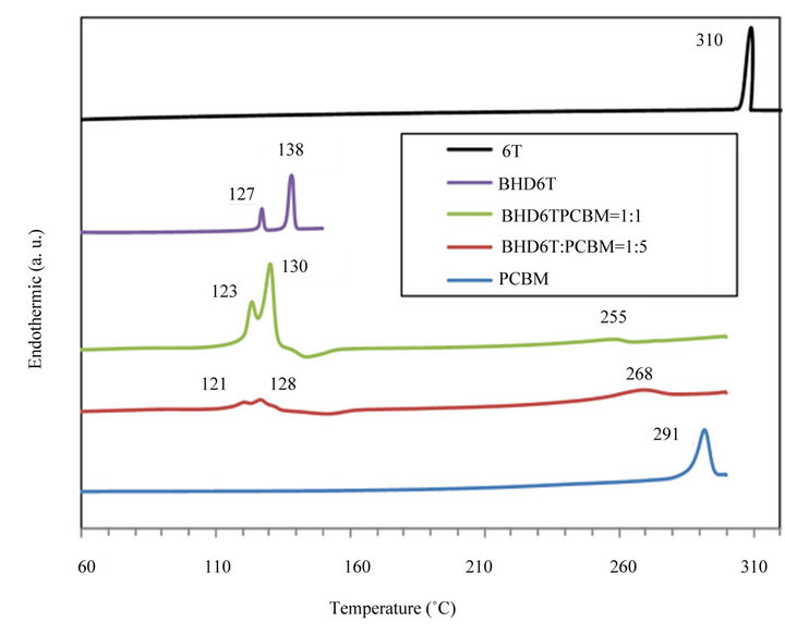
Figure 2. Differential thermal analysis (DTA) traces of 6T, BHD6T, BHD6T:PCBM (1:1), BHD6T:PCBM (1:5), and PCBM.
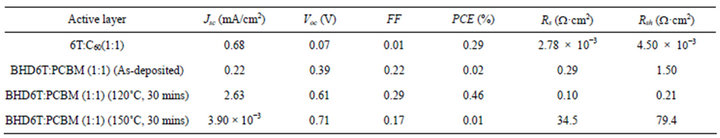
Table 1. Photovoltaic parameters of each device.
BHD6T:PCBM, BHD6T:PCBM annealed at 120˚C and BHD6T:PCBM annealed at 150˚C. The device with the as-deposited 6T:C60 active layer exhibited the lowest open-circuit voltage (Voc), fill factor (FF) and shunt resistance (Rsh). The short-circuit current density (Jsc) of the device with as-deposited 6T:C60 was lower than that of the device with BHD6T:PCBM annealed at 120˚C. The as-deposited 6T:C60 device also exhibited the lowest power conversion efficiency (PCE). For the device with the BHD6T:PCBM active layer, Voc and Rsh increased gradually with increasing temperature of the thermal annealing treatment. On the other hand, RS was increased by annealing at 120˚C, but decreased by annealing at 150˚C. Therefore, the device with BHD6T:PCBM annealed at 120˚C had a largest value of PCE in this study.
3.3. Crystallinity and Morphology
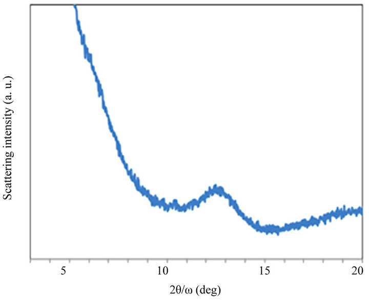
Figure 3 shows XRD patterns of the PCBM, BHD6T and BD6T:PCBM films deposited by spin-coating. These films were annealed at 120˚C. The PCBM film produced no scattering peaks [32]. This suggests that PCBM is not crystallized at 120˚C as shown in Figure 3(a). On the other hand, the BHD6T film proposed scattering peaks at 4.81˚, 7.17˚, 9.61˚, 12.07˚ and 16.91˚ as shown in Figure 3(b). Thus, it is considered that BHD6T was highly crystallized. BHD6T:PCBM produced only the scattering peaks originating from BHD6T at 4.82˚, 7.23˚, 9.64˚, 12.05˚ and 16.89˚ as shown in Figure 3(c). This result indicates that BHD6T is mainly crystallized by annealing at 120˚C in BHD6T:PCBM layer.
Figure 4 shows AFM images of the as-deposited 6T:C60 film, as-deposited BHD6T:PCBM, BHD6T PC BM annealed at 120˚C and BHD6T:PCBM annealed at 150˚C. In the surface structure of the 6T:C60 active layer, closepacked nanocrystal aggregates originating from the 6T crystal were observed [30]. These aggregates may act as effective carrier transport paths, which may result in a low Rs. In addition, the 6T:C60 layer had a rough surface owing to the aggregates, which may result in a low Rsh. On the other hand, such aggregates were not observed in all the BHD6T:PCBM films. The as-deposited BHD6T: PCBM film had a smooth surface. This suggests that BHD6T and PCBM molecules are mixed at random to produce an amorphous structure. In the BHD6T:PCBM
 (a)
(a)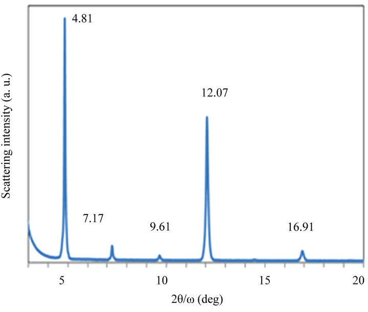 (b)
(b)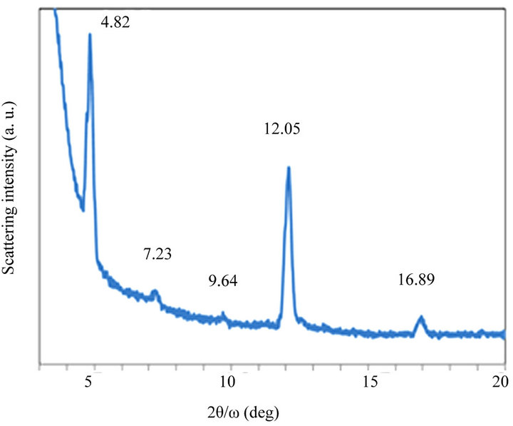 (c)
(c)
Figure 3. Out-of-plane X-ray diffraction (XRD) patterns of (a) PCBM, (b) BHD6T and (c) BHD6T:PCBM. Each sample was annealed at 120˚C for 30 mins.
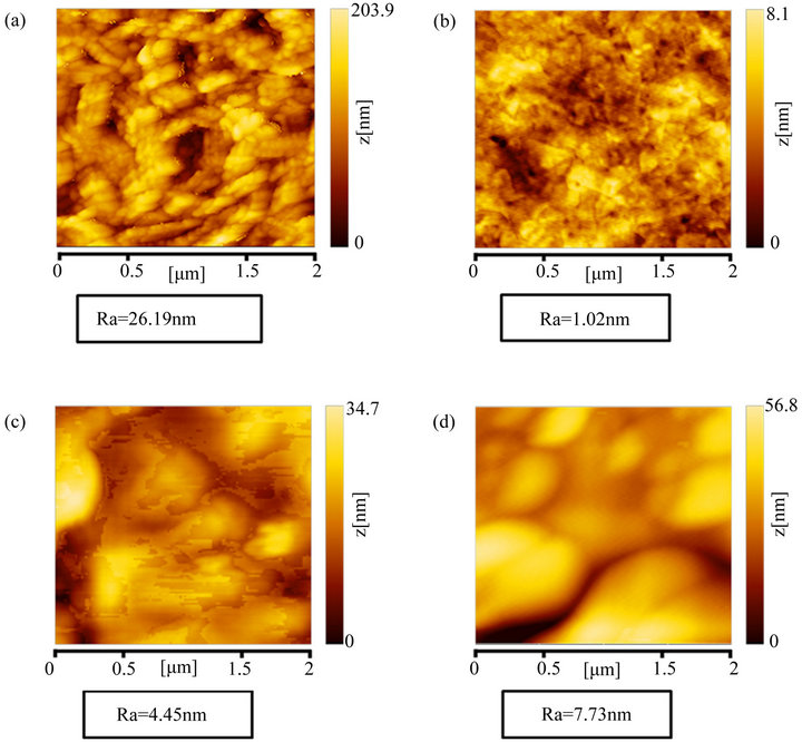
Figure 4. Atomic force microscopy (AFM) images of the 6T:C60 and BHD6T:PCBM (1:1) layers: (a) As-deposited 6T:C60 layer; (b) As-deposited BHD6T:PCBM layer; (c) BHD6T:PCBM layer annealed at 120˚C for 30 mins; (d) BHD6T:PCBM layer annealed at 150˚C for 30 mins.
film annealed at 120˚C, which is near the transition temperature of BHD6T, large grains were observed. It is assumed that these grains were microcrystals of BHD6T because the BHD6T:PCBM film annealed at 120˚C produced only scattering peaks derived from BHD6T as shown in Figure 3. These grains are considered to act as carrier transport paths.
4. Discussion
These results indicated that the device with BHD6T: PCBM annealed at 120˚C had a low Rs and a high photovoltaic performance owing to the formation of effective carrier transport paths comprising BHD6T grains. In contrast, in the active layer of BHD6T:PCBM annealed at 150˚C, isolated smooth grains were distributed on the surface. It is considered that each grain is a microcrystal of BHD6T formed by the melting and recrystallization of BHD6T by annealing at a temperature higher than its melting point of 138˚C. These grains are isolated from one another and formed grain boundaries and discontinuous carrier transport paths. In addition, these grain boundaries are considered to act as annealed at 150˚C had an extremely high Rs and a low photovoltaic performance. These results indicate that an active layer formed from highly crystalline molecules leads to the formation of close-packed microcrystal aggregates due to excessive crystallization, resulting in the low Rs, low Rsh and lower photovoltaic performance of 6T:C60. The low photovoltaic performance due to excessive crystallization can be resolved by using molecules with intricately branched alkyl side chains, such as BHD6T, for the active layer. The side chain inhibits excessive crystallization, and the crystallinity of BHD6T can be simply controlled by thermal annealing.
5. Conclusion
In summary, we clarified the effect of the side chains of materials on the morphology and photovoltaic performance of organic photovoltaic devices by comparing a BHD6T:PCBM active layer and a 6T:C60 active layer, as well as the effect of thermal annealing on the BHD6T: PCBM active layer. In the highly crystalline 6T:C60 active layer, the high crystallinity of 6T and its rough surface resulted in a low Rs and Rsh. On the other hand, the BHD6T:PCBM active layer reduced the excessive crystallization and enabled the easy control of the crystallinity in the active layer by thermal annealing owing to its side chains. These results indicate that a side chain of molecules enables the easy control of crystallinity by thermal annealing, and molecules with a side chain can be used to realize high-efficiency photovoltaic devices.
REFERENCES
- W. Wang, H. Wu, C. Yang, C. Luo, Y. Zhang, J. Chen and Y. Cao, “High-Efficiency Polymer Photovoltaic Devices from Regioregular-Poly(3-hexylthiophene-2,5-diyl) and [6,6]-Phenyl-C61-butyric Acid Methyl Ester Processed with Oleic Acid Surfactant,” Applied Physics Letters, Vol. 90, No. 18, 2007, Article ID: 183512. doi:10.1063/1.2735937
- F. Padinger, R. S. Ritberger and N. S. Sariciftci, “Effects of Postproduction Treatment on Plastic Solar Cells,” Advanced Functional Materials, Vol. 13, No. 1, 2003, pp. 85-88. doi:10.1002/adfm.200390011
- B. Sun, H. J. Snaith, A. S. Dhoot, S. Westenhoff and N. C. Greenham, “Vertically Segregated Hybrid Blends for Photovoltaic Devices with Improved Efficiency,” Journal of Applied Physics, Vol. 97, No. 1, 2005, Article ID: 014914. doi:10.1063/1.1804613
- E. Wang, L. Wang, L. Lan, C. Luo, W. Zhuang, J. Peng and Y. Cao, “High-Performance Polymer Heterojunction solar Cells of a Polysilafluorene Derivative,” Applied Physics Letters, Vol. 92, No. 3, 2008, Article ID: 033307. doi:10.1063/1.2836266
- Z. Li and C. R. McNeill, “Transient Photocurrent Measurements of PCDTBT:PC70BM and PCPDTBT:PC70BM Solar Cells: Evidence for Charge Trapping in Efficient Polymer/Fullerene Blends,” Journal of Applied Physics, Vol. 109, No. 7, 2011, Article ID: 074513. doi:10.1063/1.3573394
- F. Wudl, “The Chemical Properties of Buckminsterfullerene (C60) and the Birth and Infancy of Fulleroids,” Accounts of Chemical Research, Vol. 25, No. 3, 1992, pp. 157-161. doi:10.1021/ar00015a009
- Y. Zhang and P. W. M. Blom, “Enhancement of the Hole Injection into Regioregular Poly(3-hexylthiophene) by Molecular Doping,” Applied Physics Letters, Vol. 97, No. 8, 2010, Article ID: 083303.
- S. Ebadian, B. Gholamkhass, S. Shambayati, S. Holdcroft and P. Servati, “Effects of Annealing and Degradation on Regioregular Polythiophene-Based Bulk Heterojunction Organic Photovoltaic Devices,” Solar Energy Materials & Solar Cell, Vol. 94, No. 12, 2010, pp. 2258-2264. doi:10.1016/j.solmat.2010.07.021
- F. Zhang, K. G. Jespersen, C. Björström, M. Svensson, M. R. Andersson, V. Sundström, K. Magnusson, E. Moons, A. Yartsev and O. Inganäs, “Influence of Solvent Mixing on the Morphology and Performance of Solar Cells Based on Polyfluorene Copolymer/Fullerene Blends,” Advanced Functional Materials, Vol. 16, No. 5, 2006, pp. 667-674. doi:10.1002/adfm.200500339
- J. W. Jeong, J. W. Huh, J. I. Lee, H. Y. Chu, I. K. Han and B.-K. Ju, “Effects of Thermal Annealing on the Efficiency of Bulk-Heterojunction Organic Photovoltaic Devices,” Current Applied Physics, Vol. 10, No. 3, 2010, S520-S524. doi:10.1016/j.cap.2010.02.023
- C.-J. Ko, Y.-K. Lin and F.-C. Chen, “Microwave Annealing of Polymer Photovoltaic Devices,” Advanced Materials, Vol. 19, No. 21, 2007, pp. 3520-3523. doi:10.1002/adma.200700741
- J. Peet, C. Soci, R. C. Coffin, T. Q. Nguyen, A. Mikhailovsky, D. Moses and G. C. Bazana, “Method for Increasing the Photoconductive Response in Conjugated Polymer/Fullerene Composites,” Applied Physics Letters, Vol. 89, No. 25, 2006, Article ID: 252105. doi:10.1063/1.2408661
- H. Hoppe and N. S. Sariciftci, “Morphology of Polymer/Fullerene Bulk Heterojunction Solar Cells,” Journal of Materials Chemistry, Vol. 16, No. 1, 2006, pp. 45-61. doi:10.1039/b510618b
- S. Bertho, W. D. Oosterbaan, V. Vrindts, J. D’Haen, T. J. Cleij, L. Lutsen, J. Manca and D. Vanderzande, “Controlling the Morphology of Nanofiber-P3HT:PCBM Blends for Organic Bulk Heterojunction Solar Cells,” Organic Electronics, Vol. 10, No. 7, 2009, pp. 1248-1251.
- S. Nagamatsu, M. Misaki, M. Chikamatsu, T. Kimura, Y. Yoshida, R. Azumi, N. Tanigaki and K. Yase, “Article Crystal Structure of Friction-Transferred Poly(2,5-dioctyloxy-1,4-phenylenevinylene),” The Journal of Physical Chemistry B, Vol. 111, No. 17, 2007, pp. 4349-4354. doi:10.1021/jp067555m
- N. Ohashi, T. Miyadera, T. Taima and Y. Yoshida, “MgxC60 Fabricated by Using Mg:C60 Co-Evaporation Method for Carrier Doping,” Molecular Crystals and Liquid Crystals, Vol. 538, No. 1, 2011, pp. 193-198. doi:10.1080/15421406.2011.563723
- W. Ma, C. Yang, X. Gong, K. Lee and A. J. Heeger, “Thermally Stable, Efficient Polymer Solar Cells with Nanoscale Control of the Interpenetrating Network Morphology” Advanced Functional Materials, Vol. 15, No. 10, 2005, pp. 1617-1622. doi:10.1002/adfm.200500211
- E. Verploegen, R. Mondal, C. J. Bettinger, S. Sok, M. F. Toney and Z. Bao, “Effects of Thermal Annealing Upon the Morphology of Polymer-Fullerene Blends,” Advanced Functional Materials, Vol. 20, No. 20, 2010, pp. 3519- 3529. doi:10.1002/adfm.201000975
- S. Lilliu, T. Agostinelli, E. Pires, M. Hampton, J. Nelson and J. E. Macdonald, “Dynamics of Crystallization and Disorder during Annealing of P3HT/PCBM Bulk Heterojunctions,” Macromolecules, Vol. 44, No. 8, 2011, pp. 2725-2734. doi:10.1021/ma102817z
- B. W. Boudouris, V. Ho, L. H. Jimison, M. F. Toney, A. Salleo and R. A. Segalman, “Real-Time Observation of Poly(3-alkylthiophene) Crystallization and Correlation with Transient Optoelectronic Properties” Macromolecules, Vol. 44, No. 17, 2011, pp. 6653-6658. doi:10.1021/ma201316a
- G. Yu, J. Gao, J. C. Hummelen, F. Wudl and A. J. Heeger, “Polymer Photovoltaic Cells: Enhanced Efficiencies via a Network of Internal Donor-Acceptor Heterojunctions,” Science, Vol. 270, No. 5243, 1995, pp. 1789-1791. doi:10.1126/science.270.5243.1789
- F. Padinger, R. S. Rittberger and N. S. Saricifici, “Effects of Postproduction Treatment on Plastic Solar Cells,” Advanced Functional Materials, Vol. 13, No. 1, 2003, pp. 85-88. doi:10.1002/adfm.200390011
- A. Mishra and P. Bäuerle, “Small Molecule Organic Semiconductors on the Move: Promises for Future Solar Energy Technology,” Angewandte Chemie International Edition, Vol. 51, No. 9, 2012, pp. 2020-2067. doi:10.1002/anie.201102326
- F. Gamier, A. Yassar, R. Hajlaoui, G. U. Horowitz, F. G. Deloffre, B. Serve, S. Ries and P. Alnot, “Molecular Engineering of Organic Semiconductors: Design of SelfAssembly Properties in Conjugated Thiophene Oligomers,” Journal of the American Chemical Society, Vol. 115, No. 19, 1993, pp. 8716-8721.
- F. Garnier, R. Hajlaoui, A. El Kassmi, G. Horowitz, L. Laigre, W. Porzio, M. Armanini and F. Provasoli, “Dihexylquaterthiophene: A Two-Dimensional Liquid Crystal-Like Organic Semiconductor with High Transport Properties,” Chemistry of Materials, Vol. 10, No. 11, 1998, pp. 3334-3339. doi:10.1021/cm970704g
- A. Facchetti, J. Letizia, M. H. Yoon, M. Mushrush, H. E. Katz and T. J. Marks, “Synthesis and Characterization of Diperfluorooctyl-Substituted Phenylene-Thiophene Oligomers as n-Type Semiconductors. Molecular StructureFilm Microstructure-Mobility Relationships, Organic FieldEffect Transistors, and Transistor Nonvolatile Memory Elements,” Chemistry of Materials, Vol. 16, No. 23, 2004, pp. 4715-4727.
- N. Kiriy, A. Kiriy, V. Bocharova, M. Stamm, S. Richter, M. Plötner, W. J. Fischer, F. C. Krebs, I. Senkovska and H. J. Adler, “Conformation, Molecular Packing, and Field Effect Mobility of Regioregular β,β‘-Dihexylsexithiophene,” Chemistry of Materials, Vol. 16, No. 23, 2004, pp. 4757-4764. doi:10.1021/cm049686a
- J. A. Letizia, A. Facchetti, C. L. Stern, M. A. Ratner and T. J. Marks, “High Electron Mobility in Solution-Cast and Vapor-Deposited Phenacyl—Quaterthiophene-Based Field-Effect Transistors: Toward N-Type Polythiophenes,” Journal of the American Chemical Society, Vol. 127, No. 39, 2005, pp. 13476-13477. doi:10.1021/ja054276o
- J. Locklin, D. Li, S. C. B. Mannsfeld, E. J. Borkent, H. Meng, R. Advincula and Z. Bao, “Organic Thin Film Transistors Based on Cyclohexyl-Substituted Organic Semiconductors,” Chemistry of Materials, Vol. 17, No. 13, 2005, pp. 3366-3374. doi:10.1021/cm047851g
- J. Sakai, T. Taima and K. Saito, “Efficient Oligothiophene: Fullerene Bulk Heterojunction Organic Photovoltaic Cells,” Organic Electronics, Vol. 9, No. 5, 2008, pp. 582-590. doi:10.1016/j.orgel.2008.03.008
- M. Lu, S. Nagamatsu, Y. Yoshida, M. Chikamatsu, R. Azumi and K. Yase, “Solution-Processable Oligothiophene Derivatives with Branched Alkyl Chains and Their Thin-Film Transistor Characteristics,” Chemistry Letters, Vol. 39, No. 1, 2010, pp. 60-61. doi:10.1246/cl.2010.60
- R. Mens, S. Chambon, S. Bertho, G. Reggers, B. Ruttens, J. D’Haen, J. Manca, R. Carleer, D. Vanderzande and P. Adriaensens, “Description of the Nanostructured Morphology of [6,6]-Phenyl-C61-butyric Acid Methyl Ester (PCBM) by XRD, DSC and Solid-State NMR,” Magnetic Resonance in Chemistry, Vol. 49, No. 5, 2011, pp. 242- 247. doi:10.1002/mrc.2741