Paper Menu >>
Journal Menu >>
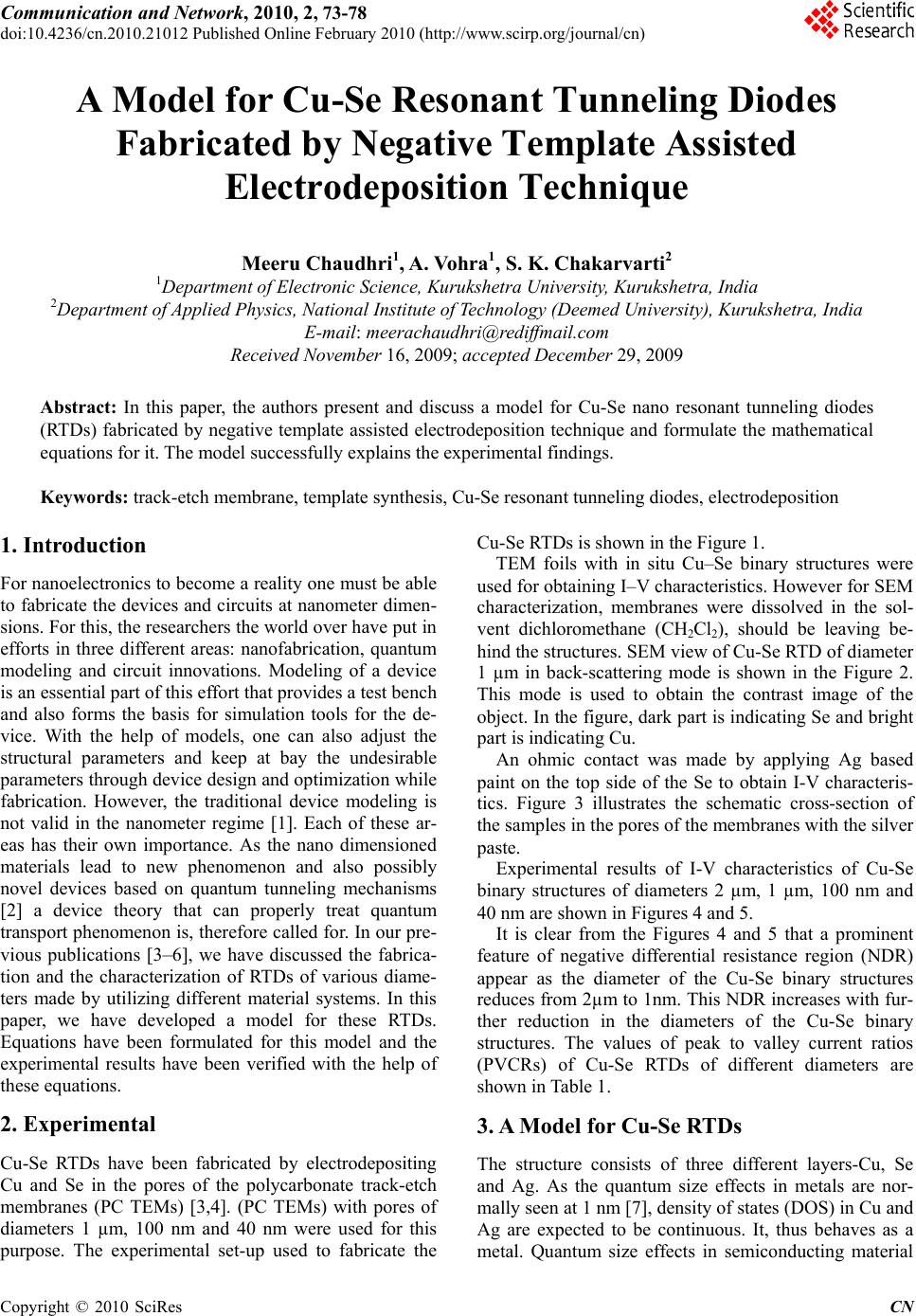 Communication and Network, 2010, 2, 73-78 doi:10.4236/cn.2010.21012 Published Online February 2010 (http://www.scirp.org/journal/cn) Copyright © 2010 SciRes CN 73 A Model for Cu-Se Resonant Tunneling Diodes Fabricated by Negative Template Assisted Electrodeposition Technique Meeru Chaudhri1, A. Vohra1, S. K. Chakarvarti2 1Department of Electronic Science, Kurukshetra University, Kurukshetra, India 2Department of Applied Physics, National Institute of Technology (Deemed University), Kurukshetra, India E-mail: meerachaudhri@redi ffmail.com Received November 16, 2009; accepted December 29, 2009 Abstract: In this paper, the authors present and discuss a model for Cu-Se nano resonant tunneling diodes (RTDs) fabricated by negative template assisted electrodeposition technique and formulate the mathematical equations for it. The model successfully explains the experimental findings. Keywords: track-etch membrane, template synthesis, Cu-Se resonant tunneling diodes, electrodeposition 1. Introduction For nanoelectronics to become a reality one must be able to fabricate the devices and circuits at nanometer dimen- sions. For this, the researchers the world over have put in efforts in three different areas: nanofabrication, quantum modeling and circuit innovations. Modeling of a device is an essential part of this effort that provides a test bench and also forms the basis for simulation tools for the de- vice. With the help of models, one can also adjust the structural parameters and keep at bay the undesirable parameters through device design and optimization while fabrication. However, the traditional device modeling is not valid in the nanometer regime [1]. Each of these ar- eas has their own importance. As the nano dimensioned materials lead to new phenomenon and also possibly novel devices based on quantum tunneling mechanisms [2] a device theory that can properly treat quantum transport phenomenon is, therefore called for. In our pre- vious publications [3–6], we have discussed the fabrica- tion and the characterization of RTDs of various diame- ters made by utilizing different material systems. In this paper, we have developed a model for these RTDs. Equations have been formulated for this model and the experimental results have been verified with the help of these equations. 2. Experimental Cu-Se RTDs have been fabricated by electrodepositing Cu and Se in the pores of the polycarbonate track-etch membranes (PC TEMs) [3,4]. (PC TEMs) with pores of diameters 1 µm, 100 nm and 40 nm were used for this purpose. The experimental set-up used to fabricate the Cu-Se RTDs is shown in the Figure 1. TEM foils with in situ Cu–Se binary structures were used for obtaining I–V characteristics. However for SEM characterization, membranes were dissolved in the sol- vent dichloromethane (CH2Cl2), should be leaving be- hind the structures. SEM view of Cu-Se RTD of diameter 1 µm in back-scattering mode is shown in the Figure 2. This mode is used to obtain the contrast image of the object. In the figure, dark part is indicating Se and bright part is indicating Cu. An ohmic contact was made by applying Ag based paint on the top side of the Se to obtain I-V characteris- tics. Figure 3 illustrates the schematic cross-section of the samples in the pores of the membranes with the silver paste. Experimental results of I-V characteristics of Cu-Se binary structures of diameters 2 µm, 1 µm, 100 nm and 40 nm are shown in Figures 4 and 5. It is clear from the Figures 4 and 5 that a prominent feature of negative differential resistance region (NDR) appear as the diameter of the Cu-Se binary structures reduces from 2µm to 1nm. This NDR increases with fur- ther reduction in the diameters of the Cu-Se binary structures. The values of peak to valley current ratios (PVCRs) of Cu-Se RTDs of different diameters are shown in Table 1. 3. A Model for Cu-Se RTDs The structure consists of three different layers-Cu, Se and Ag. As the quantum size effects in metals are nor- mally seen at 1 nm [7], density of states (DOS) in Cu and Ag are expected to be continuous. It, thus behaves as a metal. Quantum size effects in semiconducting material 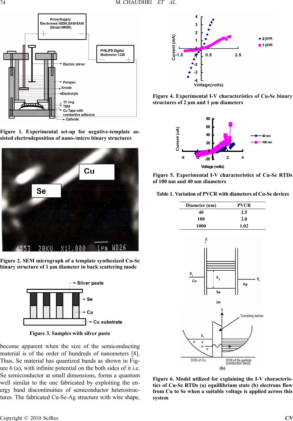 M. CHAUDHRI ET AL. Copyright © 2010 SciRes CN 74 Figure 1. Experimental set-up for negative-template as- sisted electrodeposition of nano-/micro binary structures Figure 2. SEM micrograph of a template synthesized Cu-Se binary structure of 1 µm diameter in back scattering mode Figure 3. Samples with silver paste become apparent when the size of the semiconducting material is of the order of hundreds of nanometers [8]. Thus, Se material has quantized bands as shown in Fig- ure 6 (a), with infinite potential on the both sides of it i.e. Se semiconductor at small dimensions, forms a quantum well similar to the one fabricated by exploiting the en- ergy band discontinuities of semiconductor heterostruc- tures. The fabricated Cu-Se-Ag structure with wire shape, Figure 4. Experimental I-V characteristics of Cu-Se binary structures of 2 µm and 1 µm diameters -20 0 20 40 60 80 -4-20 2 4 Vo ltage (volts) Current (uA) 40 nm 100 nm Figure 5. Experimental I-V characteristics of Cu-Se RTDs of 100 nm and 40 nm diameters Table 1. Variation of PVCR with diameters of Cu-Se devices Diameter (nm) PVCR 40 2.5 100 2.0 1000 1.02 (b) Figure 6. Model utilized for explaining the I-V characteris- tics of Cu-Se RTDs (a) equillibrium state (b) electrons flow from Cu to Se when a suitable voltage is applied across this system  M. CHAUDHRI ET AL. Copyright © 2010 SciRes CN 75 hence, forms one dimensional RTD with Cu as emitter, Ag as collector and Se as a potential well. On applying a voltage across the device, the band diagrams can be re- drawn as shown in Figure 6(b). The electrons from the Cu electrode tunnel to the empty states in the conduction band of Se. The electrons in the well stay at a particular energy level until these electrons get enough energy to jump to the next higher energy level. These electron waves reflect back and forth between the two walls of the well and interfere, causing the change in the ampli- tude of the wave. When the energy of the electrons is equal to the energy of the quantized level in the well, the two waves interfere constructively and resonance of the electron wave takes place, which results in maximum transmission of electrons. The accumulation of electrons in the well thus results in a decrease in the current up to valley point current of the I-V curve. Based on this model of quantization of energy levels, the I-V behavior of the Cu-Se structures has been ex- plained. The energy levels in Cu-Se-Ag structures can be drawn as in Figure 7. The bulk behavior of the Cu-Se binary structures of 2 µm can be explained by the energy level diagram of Figure 7 (a) where the energy levels are continuous. However, as the dimensions of the device are reduced, quantized energy levels appear in Se semiconductor and a negative differential resistance region starts appearing. This is shown in Figure 7 (b). On reducing the diameter further, the negative differential resistance region in- creases and this is illustrated in Figure 7 (c). The energy band diagrams in Figures. 7 (b) and (c) show the increase in spacing in energy levels in the conduction band of the Se with decrease in the dimensions (diameter) of the fab- ricated binary structures. Further, the cut-in voltages of the devices increase with decrease in diameters of the device. This indicates an increase in the Schottky barrier height due to increase in band gap of Se as the device dimensions are reduced. Various workers [9,10] have reported an increase in band gap with reduction in dimensions. A similar behavior is expected for Se as well and has been shown in Figures 7(a), (b) and (c). 4. Theor etical Analysis of Experimental Results In this section, the authors intend to correlate some of the experimental observations. Figures 4 and 5 and Table 1 indicate that there is 1) an increase in cut-in voltage as the diameters of the device is decreased 2) The PVCR increases with decrease in diameters of the device. 4.1 Increase in Cut-In Voltage The increase in cut in voltage as seen in Figs. 4 and 5 can be explained due to increase in band gap. Such an in- crease in band gap with decrease in diameter is reported in literature [10–12]. As a metal is brought in contact with a semiconductor, a barrier will be formed at the metal-semiconductor in- terface. The height of the barrier is governed by metal work function and the electron affinity of the semicon- ductor. The voltage required to increase the energy of electrons on the metal side to overcome the barrier is cut-in voltage. The cut-in voltage and the band gap of the semiconductor are related as [13]. qb=Eg - q (m -) (1) where Eg is band gap of the semiconductor qm is work-function of the metal qb is Schottky barrier height at the metal- semiconductor contact q is electron affinity of the semiconductor Figure 7. Energy band diagrams and corresponding I-V characteristics of Cu-Se resonant tunneling diodes of dif- ferent diameters illustrating the emergence of quantum size effects (a) bulk effect (b & c) quantum size effects 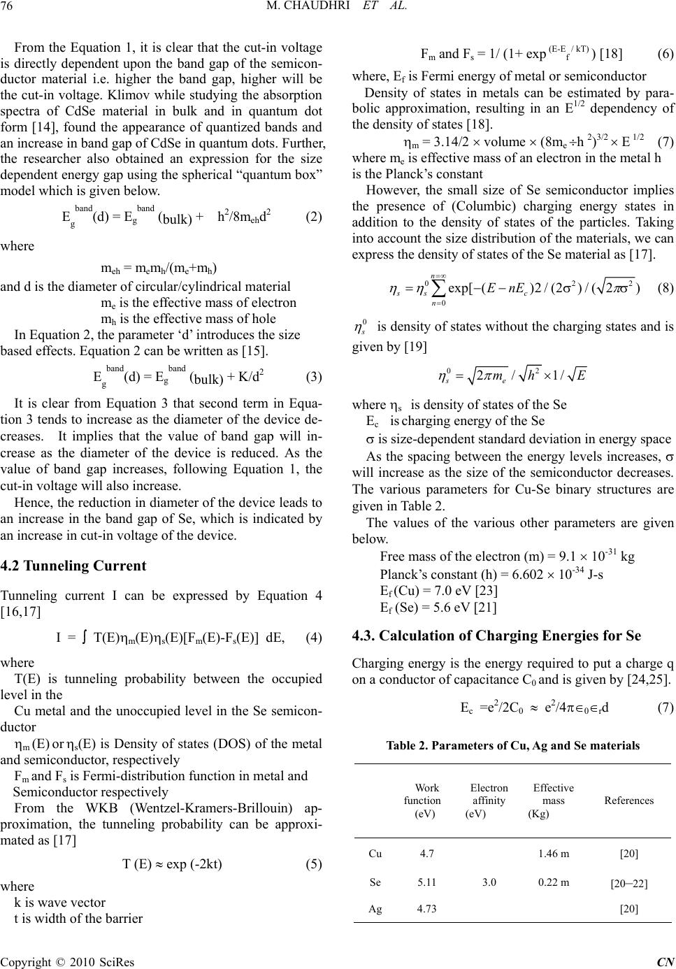 M. CHAUDHRI ET AL. Copyright © 2010 SciRes CN 76 From the Equation 1, it is clear that the cut-in voltage is directly dependent upon the band gap of the semicon- ductor material i.e. higher the band gap, higher will be the cut-in voltage. Klimov while studying the absorption spectra of CdSe material in bulk and in quantum dot form [14], found the appearance of quantized bands and an increase in band gap of CdSe in quantum dots. Further, the researcher also obtained an expression for the size dependent energy gap using the spherical “quantum box” model which is given below. Eg band(d) = Eg band (bulk) + h2/8mehd2 (2) where meh = memh/(me+mh) and d is the diameter of circular/cylindrical material me is the effective mass of electron mh is the effective mass of hole In Equation 2, the parameter ‘d’ introduces the size based effects. Equation 2 can be written as [15]. Eg band(d) = Eg band (bulk) + K/d2 (3) It is clear from Equation 3 that second term in Equa- tion 3 tends to increase as the diameter of the device de- creases. It implies that the value of band gap will in- crease as the diameter of the device is reduced. As the value of band gap increases, following Equation 1, the cut-in voltage will also increase. Hence, the reduction in diameter of the device leads to an increase in the band gap of Se, which is indicated by an increase in cut-in voltage of the device. 4.2 Tunneling Current Tunneling current I can be expressed by Equation 4 [16,17] I = T(E)m(E)s(E)[Fm(E)-Fs(E)] dE, (4) where T(E) is tunneling probability between the occupied level in the Cu metal and the unoccupied level in the Se semicon- ductor m (E) or s(E) is Density of states (DOS) of the metal and semiconductor, respectively Fm and Fs is Fermi-distribution function in metal and Semiconductor respectively From the WKB (Wentzel-Kramers-Brillouin) ap- proximation, the tunneling probability can be approxi- mated as [17] T (E) exp (-2kt) (5) where k is wave vector t is width of the barrier Fm and Fs = 1/ (1+ exp (E-E f / kT) ) [18] (6) where, Ef is Fermi energy of metal or semiconductor Density of states in metals can be estimated by para- bolic approximation, resulting in an E1/2 dependency of the density of states [18]. m = 3.14/2 volume (8me h 2)3/2 E 1/2 (7) where me is effective mass of an electron in the metal h is the Planck’s constant However, the small size of Se semiconductor implies the presence of (Columbic) charging energy states in addition to the density of states of the particles. Taking into account the size distribution of the materials, we can express the density of states of the Se material as [17]. 022 0 exp[()2 / (2) / (2) n ss c n EnE (8) 0 s is density of states without the charging states and is given by [19] 02 2/ 1/ se mh E where s is density of states of the Se Ec is charging energy of the Se is size-dependent standard deviation in energy space As the spacing between the energy levels increases, will increase as the size of the semiconductor decreases. The various parameters for Cu-Se binary structures are given in Table 2. The values of the various other parameters are given below. Free mass of the electron (m) = 9.1 10-31 kg Planck’s constant (h) = 6.602 10-34 J-s Ef (Cu) = 7.0 eV [23] Ef (Se) = 5.6 eV [21] 4.3. Calculation of Charging Energies for Se Charging energy is the energy required to put a charge q on a conductor of capacitance C0 and is given by [24,25]. Ec =e2/2C0 e 2/40rd (7) Table 2. Parameters of Cu, Ag and Se materials Work function (eV) Electron affinity (eV) Effective mass (Kg) References Cu 4.7 1.46 m [20] Se 5.11 3.0 0.22 m [20–22] Ag 4.73 [20] 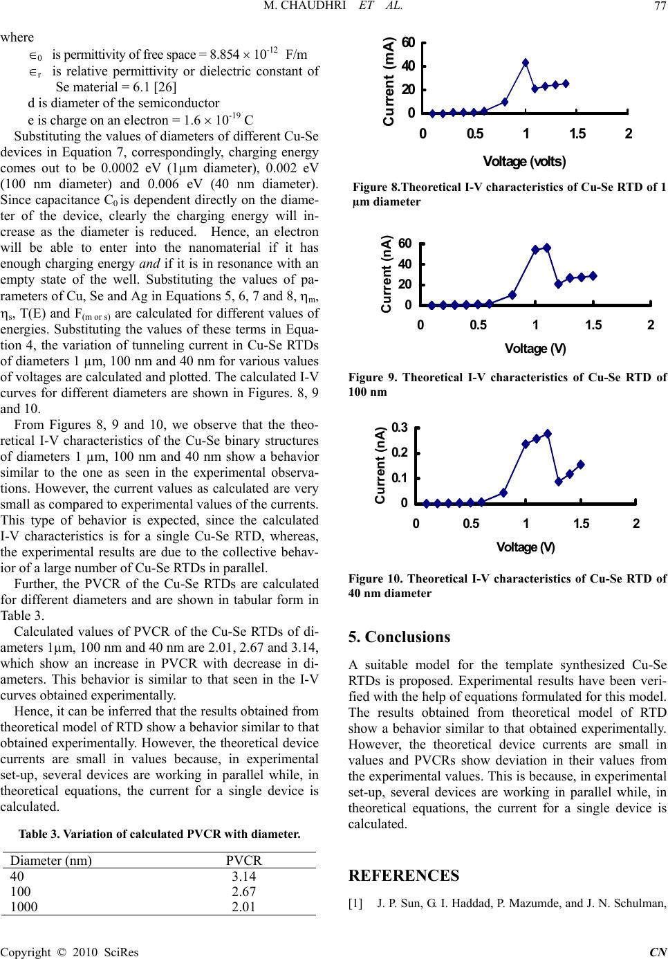 M. CHAUDHRI ET AL. Copyright © 2010 SciRes CN 77 where 0 is permittivity of free space = 8.854 10-12 F/m r is relative permittivity or dielectric constant of Se material = 6.1 [26] d is diameter of the semiconductor e is charge on an electron = 1.6 10-19 C Substituting the values of diameters of different Cu-Se devices in Equation 7, correspondingly, charging energy comes out to be 0.0002 eV (1µm diameter), 0.002 eV (100 nm diameter) and 0.006 eV (40 nm diameter). Since capacitance C0 is dependent directly on the diame- ter of the device, clearly the charging energy will in- crease as the diameter is reduced. Hence, an electron will be able to enter into the nanomaterial if it has enough charging energy and if it is in resonance with an empty state of the well. Substituting the values of pa- rameters of Cu, Se and Ag in Equations 5, 6, 7 and 8, m, s, T(E) and F(m or s) are calculated for different values of energies. Substituting the values of these terms in Equa- tion 4, the variation of tunneling current in Cu-Se RTDs of diameters 1 µm, 100 nm and 40 nm for various values of voltages are calculated and plotted. The calculated I-V curves for different diameters are shown in Figures. 8, 9 and 10. From Figures 8, 9 and 10, we observe that the theo- retical I-V characteristics of the Cu-Se binary structures of diameters 1 µm, 100 nm and 40 nm show a behavior similar to the one as seen in the experimental observa- tions. However, the current values as calculated are very small as compared to experimental values of the currents. This type of behavior is expected, since the calculated I-V characteristics is for a single Cu-Se RTD, whereas, the experimental results are due to the collective behav- ior of a large number of Cu-Se RTDs in parallel. Further, the PVCR of the Cu-Se RTDs are calculated for different diameters and are shown in tabular form in Table 3. Calculated values of PVCR of the Cu-Se RTDs of di- ameters 1µm, 100 nm and 40 nm are 2.01, 2.67 and 3.14, which show an increase in PVCR with decrease in di- ameters. This behavior is similar to that seen in the I-V curves obtained experimentally. Hence, it can be inferred that the results obtained from theoretical model of RTD show a behavior similar to that obtained experimentally. However, the theoretical device currents are small in values because, in experimental set-up, several devices are working in parallel while, in theoretical equations, the current for a single device is calculated. Table 3. Variation of calculated PVCR with diameter. Diameter ( nm ) PVCR 40 3.14 100 2.67 1000 2.01 0 20 40 60 00.5 1 1.5 2 V o ltag e (vo lts) C u rrent (mA) Figure 8.Theoretical I-V characteristics of Cu-Se RTD of 1 µm diameter 0 20 40 60 00.511.52 Vo ltage (V) Current (nA) Figure 9. Theoretical I-V characteristics of Cu-Se RTD of 100 nm 0 0.1 0.2 0.3 00.511.52 Voltage (V) Current (nA) Figure 10. Theoretical I-V characteristics of Cu-Se RTD of 40 nm diameter 5. Conclusions A suitable model for the template synthesized Cu-Se RTDs is proposed. Experimental results have been veri- fied with the help of equations formulated for this model. The results obtained from theoretical model of RTD show a behavior similar to that obtained experimentally. However, the theoretical device currents are small in values and PVCRs show deviation in their values from the experimental values. This is because, in experimental set-up, several devices are working in parallel while, in theoretical equations, the current for a single device is calculated. REFERENCES [1] J. P. Sun, G. I. Haddad, P. Mazumde, and J. N. Schulman,  M. CHAUDHRI ET AL. Copyright © 2010 SciRes CN 78 Proceedings of the IEEE, Vol. 86, No. 4, pp. 641, 1998. [2] O. I. Mićić and A. J. Nozik, in Hari Singh Nalwa (Ed.), Colloidal Quantum Dot of III-V Semiconductors, Hand- book of Nanostructured Mateials and Nanotechnology, Academic Press, 2000. [3] M. Chaudhri, A. Vohra, S. K. Chakarvarti, and R. Kumar, J. mater. Sci., Mater Electron, Vol. 17, pp. 189, 2006. [4] M. Chaudhri, A. Vohra, and S. K. Chakarvarti, J. Mater. Sci., Mater Electron, Vol. 17, pp. 993, 2006. [5] M. Chaudhri, A. Vohra, and S. K. Chakarvarti, Physica E, Vol. 40, pp. 849, 2008. [6] M. Chaudhri, A. Vohra, and S. K. Chakarvarti, Mater. Sci. Engg. B, Vol. 149, No. 7, pp. 641, 2008. [7] H. D. Vladimir Gavryushin, Functional Combinations in Solid States, 2002. http://www.mtmi.vu.lt/pfk/funkc_dari- niai/index.html. [8] V. V. Moshchalkov, V. Bruyndoncx, L. L. Van, M. J. Van Bael, Y. Bruynseraede, and A. Tonomura, in Hari Singh Nalwa (Ed.), Quantization and Confinement Phenomena in Nanostructured Superconductors, Handbook of Nanos- tructured Mateials and Nanotechnology, Academic Press, 2000. [9] Y. J. Choi, I. S. Hwang, J. H. Park, S. Nahm, and J. G. Park, Nanotechnology, Vol. 17, pp. 3775, 2006. [10] J. Heremans, C. M. Thrush, Y. M. Lin, S. Cronin, Z. Zhang, M. S. Dresselhaus, and J. F. Mansfield, Phys. Rev. B, Vol. 61, pp. 2921, 2000. [11] M. Li and J. C. Li, , Mater. Lett. Vol. 60, pp. 2526, 2006. [12] S. Cronin, Z. Zhang, and M. S. Dresselhaus, Phys. Rev. B, Vol. 61, No. 4, pp. 2921, 2000. [13] S. M. Sze, Physics of Semiconductor Devices. New York, Wiley, 1981. [14] V. I. Klimov, Vol. 28, pp. 215, 2003. [15] S. Ogut, J. R. Chelikowsky, and S. G. Louie, Phys. Rev. Lett., Vol. 79, pp. 1770, 1997. [16] A. Sigurdardottir, V. Krozer, and H. L. Hartnage, Appl. Phys. Lett., Vol. 67, No. 22, pp. 3313, 1995. [17] S. H. Kim, , G. Markovich, S. Rezvani, S. H. Choi, S. H., K. L. K. L. Wang, and J. R. Heath, Appl. Phys. Lett., pp. 317, 1999. [18] B. G. Streetman, “Solid state electronic devices,” Pren- tice-Hall of India Private Limited, New Delhi, 1994. [19] B. V. Zeghbroeck, “Principles of semiconductor devices,” 2004. http://ece-www.colorado.edu/~bart/book. [20] P. A. Tipler and R. A. Liewellyn, Modern Physics, 3rd Edtion, W. H. Freeman, 1999. [21] K. Barbalace, 2006. http://Klbprouctions.com/Periodic Table of Elements-Selenium-Se, Environmental Chemis- try.com, 1995–2006. Accessed online: 7/13/2006. http:// Environmental Chemistry.com//yogi/Periodic/Se.html. [22] C. M. Fang, R. A. De Groot, and G. A. wiegers, Journal of Physics and Chemistry of Solids, Vol. 63, pp. 457, 2002. [23] N. W. Ashcroft and N. D. Mermin, Solid State Physics, Saunders, 1976. [24] A. J. Quinn, P. Beecher, D. Iacopino, L. Floyd, G. De- Marzi, E. V. Shechenko, H. Weller, and R G. edmond, Small 1, 613. Vol. 1, pp. 613, 2005. [25] S. Möller, H. Buhmann, S. F. Godijn, and L. W. Molen- kamp, Phys. Rev. Lett., Vol. 81, No. 23, pp. 5197, 1998. [26] Dielectric Constant References Guide: http://www.asi- instr.com/technal/Dielectric%20Constants.htm. |