Circuits and Systems
Vol. 4 No. 2 (2013) , Article ID: 29886 , 10 pages DOI:10.4236/cs.2013.42029
MIMO Hardware Simulator: Algorithm Design for Heterogeneous Environments
Institute of Electronics and Telecommunications of Rennes, Rennes, France
Email: bachir.habib@insa-rennes.fr
Copyright © 2013 Bachir Habib et al. This is an open access article distributed under the Creative Commons Attribution License, which permits unrestricted use, distribution, and reproduction in any medium, provided the original work is properly cited.
Received November 30, 2012; revised February 2, 2013; accepted February 9, 2013
Keywords: Hardware Simulator; MIMO Radio Channel; FPGA; 802.11ac Signal; Time-Varying TGn Channel Models
ABSTRACT
A wireless communication system can be tested either in actual conditions or by a hardware simulator reproducing actual conditions. With a hardware simulator it is possible to freely simulate a desired type of a radio channel and making it possible to test “on table” mobile radio equipment. This paper presents an architecture for the digital block of a hardware simulator of MIMO propagation channels. This simulator can be used for LTE and WLAN IEEE 802.11ac applications, in indoor and outdoor environments. However, in this paper, specific architecture of the digital block of the simulator is presented to characterize a scenario indoor to outdoor using TGn channel models. The switching between each environment in the scenario must be made in a continuous manner. Therefore, an algorithm is designed to pass from a considered impulse response in the environment to another in other environment. The architecture of the digital block of the hardware simulator is presented and implemented on a Xilinx Virtex-IV FPGA. Moreover, the impulse responses are transferred into the simulator. The accuracy, the occupation on the FPGA and the latency of the architecture are analyzed.
1. Introduction
Wireless communication systems may offer high data bit rates by achieving a high spectral efficiency using Multiple-Input Multiple-Output (MIMO) techniques. MIMO systems make use of antenna arrays simultaneously at both transmitter and receiver sites to improve the capacity and/or the system performance. However, the transmitted electromagnetic waves interact with the propagation environment. Thus, it is necessary to take into account the main propagation parameters during the design of the future communication systems. The current communication standards indicate a clear trend in industry toward supporting MIMO functionality. In fact, several studies published recently present systems that reach a MIMO order of 8 × 8 and higher [1]. This is made possible by advances at all levels of the communication platform, as the monolithic integration of antennas [2] and the simulator platforms design [3].
The objective of our work concerns the channel models and the digital block of the simulator. The design of the RF blocks was completed in a previous project [4].
The channel models can be obtained from standard channel models, as the TGn IEEE 802.11n [5] and the LTE models [6], or from real measurements conducted with the MIMO channel sounder designed and realized at IETR [7].
In the MIMO context, little experimental results have been obtained regarding time-variations, partly due to limitations in channel sounding equipment [8]. However, theoretical models of impulse responses of time-varying channels can be obtained using Rayleigh fading [9,10].
Tests of a radio communication system, conducted under actual conditions are difficult, because tests taking place outdoors, for instance, are affected by random movements or even by the weather. However, with hardware simulators, it is possible to very freely simulate desired types of radio channels. Moreover, a hardware simulator provides the necessary processing speed and real time performance, as well as the possibility to repeat the tests for any MIMO system. Thus, a hardware simulator can be used to compare the performance of various radio communication systems in the same desired test conditions.
These simulators are standalone units that provide the fading signal/signals of SISO/MIMO channel in the form of analog or digital samples. Some MIMO hardware simulators are proposed by industrial companies like Spirent (VR5) [11], Azimuth (ACE), Elektrobit (Propsim F8) [12], but they are quite expensive.
With continuing increase of the Field Programmable Gate Array (FPGA) capacity, entire baseband systems can be mapped onto faster FPGAs for more efficient prototyping, testing and verification. Larger and faster FPGAs permit the integration of a channel simulator along with the receiver noise simulator and the signal processing blocks for rapid and cost-effective prototyping and design verification. As shown in [13], the FPGAs provide the greatest design flexibility and the visibility of resource utilization.
The MIMO hardware simulator realized at IETR is reconfigurable with sample frequencies not exceeding 200 MHz, which is the maximum value for FPGA Virtex-IV. The 802.11ac signal provides a sample frequency of 200 MHz. Thus, it is compatible with the FPGA Virtex-IV. However, in order to exceed 200 MHz for the sample frequency, more performing FPGA as Virtex-VII can be used [3]. The simulator is able to accept input signals with wide power range, between −50 and 33 dBm, which implies a power control for the input signals.
At IETR, several architectures of the digital block of a hardware simulator have been studied, in both time and frequency domains [4]. Typically, wireless channels are commonly simulated using finite impulse response (FIR) filters, as in [14-16]. The FIR filter output signal is a convolution between a channel impulse response and a fed signal in such a manner that the signal delayed by different delays is weighted by the channel coefficients, i.e. tap coefficients, and the weighted signal components are summed up. The channel coefficients are periodically modified to reflect the behavior of an actual channel. Nowadays, different approaches have been widely used in filtering, such as distributed arithmetic (DA) and canonical signed digits (CSDs) [17].
Using FIR filter in a channel simulator has however a limitation. With a FPGA Virtex-IV, it is impossible to implement a FIR filter with more than 192 multipliers (impulse response with more than 192 taps).
To simulate an impulse response with more than 192 taps, the Fast Fourier Transform (FFT) module can be used. With a FPGA Vitrex-IV, the size N of the FFT module can reach 65536 samples. Thus, several frequency architectures have been considered and tested [17]. However, their disadvantages are high latency and high occupation on FPGA.
In this paper, the number of taps is limited to 18 for each SISO channel, thus, to 18 × 4 taps for the 2 × 2 MIMO channel. Therefore, the time domain architecture is considered because the total number of taps does not exceed 192.
The main contributions of the paper are:
• In general, the channel impulse responses can be presented in baseband with its complex values, or as real signals with limited bandwidth B between fc – B/2 and fc + B/2, where fc is the carrier frequency. In this paper, to eliminate the fc and the complex multiplication, the hardware simulation operates between Δ and B + Δ, where Δ depends on the band-pass filters (RF and IF). The value Δ is introduced to prevent spectrum aliasing. The use of real impulse response allows the reduction by 2 of the FIR filters size and by 4 the number of multipliers. Thus, within the same FPGA, MIMO channels with larger number of antennas can be simulated.
• Tests have been made for indoor [18] and outdoor [19, 20] fixed environments using standard channel models. In this paper, tests are made with scenario that switches between indoor environment and another, or between indoor and outdoor environments to simulate heterogeneous networks [21]. In this context, an algorithm is proposed to switch between the environments in a continuous manner.
• To decrease the number of multipliers on the FPGA and to switch from one environment to another, a solution is proposed to control the change of delays in architecture for time-varying channel.
The rest of this paper is organized as follows. Section 2 presents the channel models and the scenario proposed for the test. Section 3 describes the algorithm designed to switch between environments. Section 4 presents the designed architecture of the digital block of the simulator and its implementation summary on the FPGA. In Section 5, the accuracy of the output signals of the architecture are analyzed. The output SNR for the entire scenario is provided. Lastly, Section 6 gives concluding remarks and prospects.
2. Channel Description
2.1. Proposed Scenario
The proposed scenario covers indoor and indoor-to-outdoor environments at different environmental speeds. They consider the movements from an environment to another using an 802.11ac signal which has a 200 MHz sampling frequency (fs) at a central frequency of 5 GHz. Thus, the sampling period Ts = 5 ns.
A person moves from an office environment to a large indoor environment, then to an outdoor environment. For this scenario, the TGn channel model B, C and E cover the entire channel. Thus, three environments in this scenario are considered.
Figure 1 and Table 1 present the scenario and the movement of the person in it.
v is the mean environmental speed, fd is the Doppler frequency, fref is the refresh frequency between two suc-
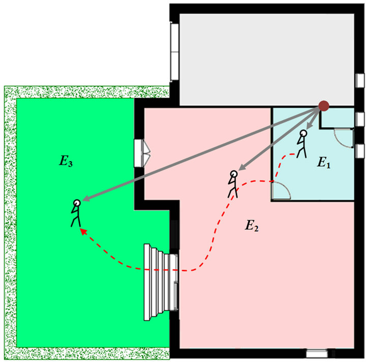
Figure 1. Proposed scenario.
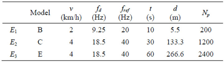
Table 1. Scenario description.
cessive MIMO profiles, t is the time duration of movements in the considered environment, d is the distance traveled and Np = t × fref is the number of profiles in each environment. fd is equal to:
 (1)
(1)
where c is the celerity. fref is chosen > 2·fd to respect the Nyquist-Shannon sampling theorem.
TGn channel models [5] have a set of 6 profiles, labeled A to F, which cover all the scenarios for WLAN applications. Each model has a number of clusters. Each cluster corresponds to specific tap delays which overlap each other in certain cases. The relative power of each tap of the impulse response for the considered TGn channel models are presented in Table 2 by taking the Lineof-Sight (LOS) path as reference.
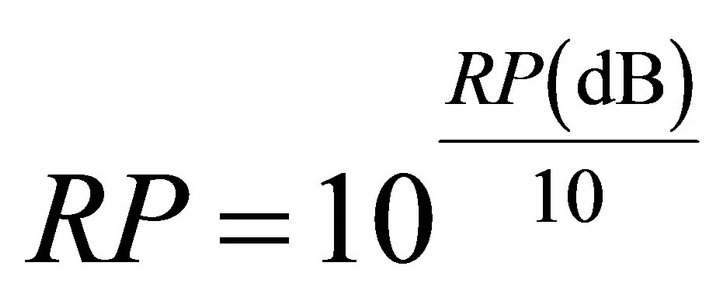
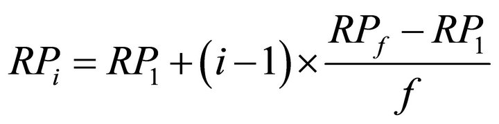
RP is the linear relative power; it can be obtained from the relative power in (dB) by:
 (2)
(2)
The maximum relative delay for the last tap for model B is 80 (ns), for model C is 200 (ns) and for model E is 730 (ns). Each tap of each model considers reflection of the wave in the environment. Thus, the scenarios in this
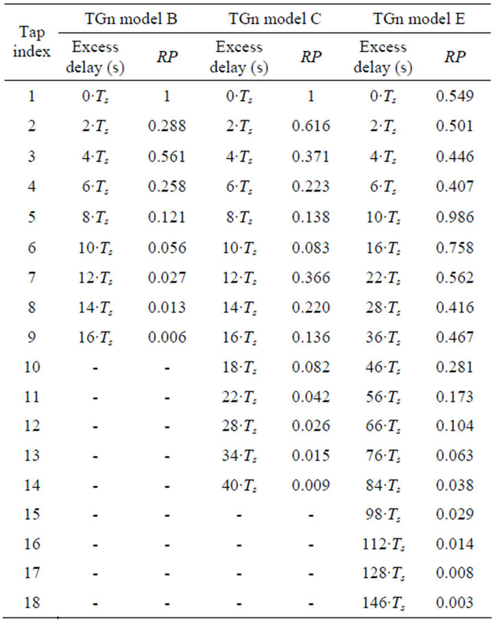
Table 2. Path loss for the considered TGn models.
paper are considered as scenario models.
Model E is considered for a typical large open space (indoor and outdoor) in Non-Line-of-Sight (NLOS) conditions. Model C represents a large indoor environment in NLOS conditions. Lastly, Model B is used for typical office environments in NLOS conditions.
2.2. Time-Varying 2 × 2 MIMO Channel
In this section, we present the method used to obtain a model of a time variant channel, using the Rayleigh fading. A 2 × 2 MIMO Rayleigh fading channel [22,23] is considered. The MIMO channel matrix H can be characterized by two parameters:
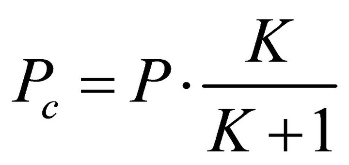
1) The relative power Pc of constant channel components corresponds to LOS paths.
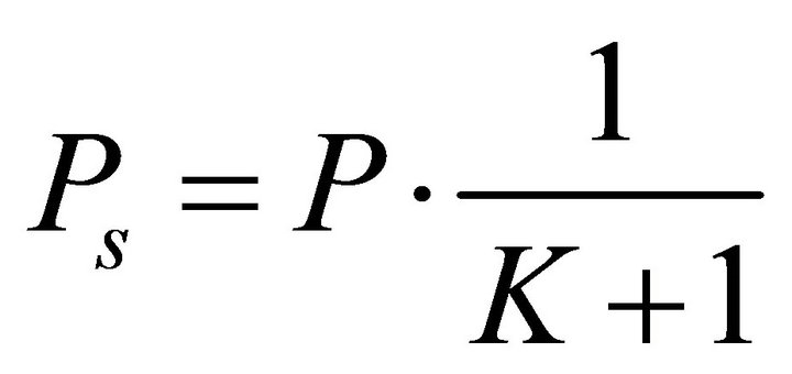
2) The relative power Ps of the channel scattering components corresponds to NLOS paths.
The ratio Pc/Ps is called Ricean K-factor.
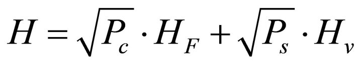
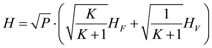
Assuming that all the elements of the MIMO channel matrix H are Rice distributed, it can be expressed for each tap by:
 (3)
(3)
where HF and HV are the constant and the scattered channel matrices respectively.
The total relative received power is P = Pc + Ps. Therefore:
 (4)
(4)
 (5)
(5)
If we replace Equations (4) and (5) in Equation (3) we obtain:
 (6)
(6)
To obtain a Rayleigh fading channel, K is equal to zero, so H can be written as:
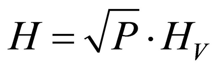 (7)
(7)
P is derived from Table 2 for each tap. For 2 transmit and 2 receive antennas:
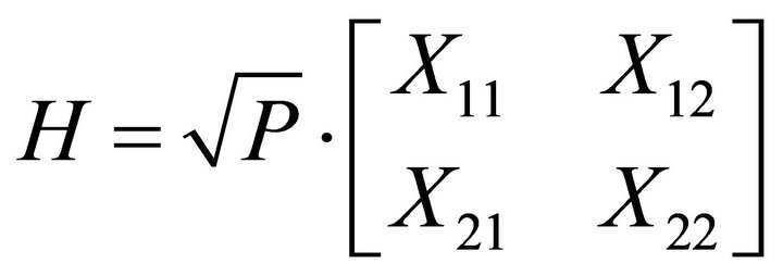 (8)
(8)
where Xij (i-th receiving and j-th transmitting antenna) are correlated zero-mean, unit variance, complex Gaussian random variables as coefficients of the variable NLOS (Rayleigh) matrix HV.
To obtain correlated Xij elements, a product-based model is used [23]. This model assumes that the correlation coefficients are independently derived at each end of the link:
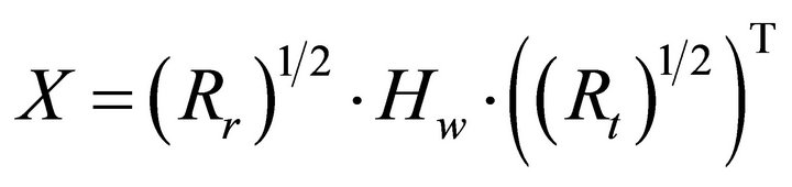 (9)
(9)
Hw is a matrix of independent zero mean, unit variance, complex Gaussian random variables. Rr and Rt are the receive and transmit correlation matrices. They can be written by:
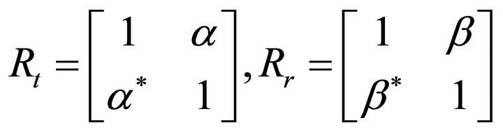 (10)
(10)
where α is the correlation between channels (between their average signal gain) at two receives antennas, but originating from the same transmit antenna (SIMO). It is the correlation between channels that have the same Angle of Departure (AoD). β is the correlation coefficient between channels at two transmit antennas that have the same receive antenna (MISO).
The use of this model has two conditions:
1) The correlations between channels at two receive (resp. transmit) antennas are independent from the Rx (resp. Tx) antenna.
2) If s1 (resp. s2) is the cross-correlation between antennas AoD (resp. AoA) at the same side of the link, then: 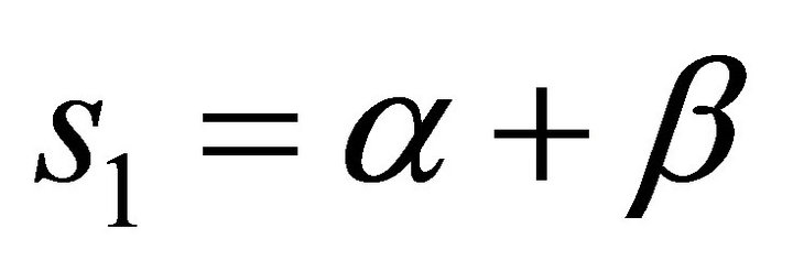 and
and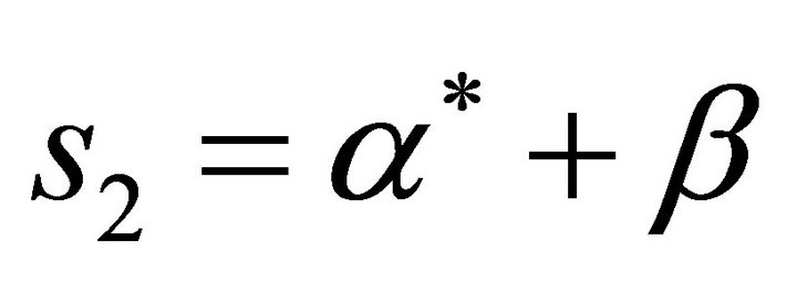 .
.
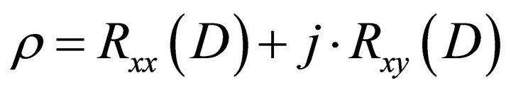
α and β are expressed by ρ:
 (11)
(11)
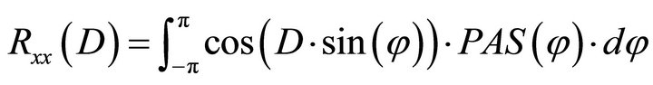
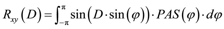
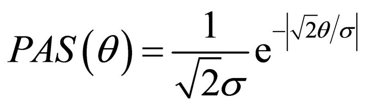
where D = 2πd/λ, d = 0.5λ is the distance between two successive antennas, λ is the wavelength and Rxx and Rxy are the real and imaginary parts of the cross-correlation function of the considered correlated angles:
 (12)
(12)
 (13)
(13)
The PAS (Power Angular Spectrum) closely matches the Laplacian distribution [24,25]:
 (14)
(14)
where σ is the standard deviation of the PAS.
3. Algorithm Design
The switch between the environments must be made in continuous manner.
Between E1 and E2 for example, the person speed begins accelerating from 2 (km/h) to 4 (km/h). Thus, we consider a mean environmental speed for each environment.
After applying the method used to obtain a 2 × 2 MIMO time-varying channel presented in Section 2.2, Table 3 presents the relative powers (RP) of the last impulse response of h11 in E1, the first h11 in E2, the last h11 in E2 and the first h11 in E3.
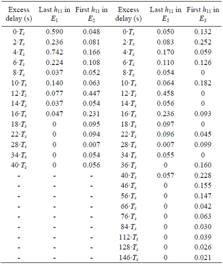
Table 3. Relative power for the considered switching impulse responses for h11.
To switch from 9 taps (E1) with a maximum delay of 16Ts to 14 taps (E2) with a maximum delay of 40Ts, an algorithm is proposed. Two parameters are considered: the delay of the taps of the impulse responses and their RP:
1) As presented in Table 2, the excess delays of the 9 taps in E1 are equal to the first 9 taps excess delay of E2. Therefore, we completed the impulse responses RP vectors of h11 in E1 by 14 − 9 = 5 zeros that corresponds to the excess delay of E2, as presented in Table 3.
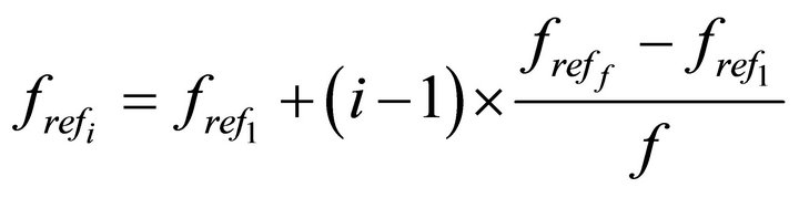
2) To pass from RP of last h11 in E1 (RP1) to first h11 in E2 (RPf), a relation is proposed to increase the RP on each fref :
 (15)
(15)
where i is an integer that varies from 2 to f − 1. fref also changes, as presented in Table 1. It passes from 20 Hz
 to 40 Hz
 :
:
 (16)
(16)
f is chosen equal to 80. In fact, the average  is equal to 30 Hz. In this case, 80/30 = 2.66 s needed time to switch between the impulse responses which is sufficient to consider it in continuous manner.
Figure 2 presents the switch between the last h11 in E1 and the first h11 in E2 for the 80 profile of h11.
To switch from the last h11 in E2 to the first h11 in E3, the same previous method is used. However, in this case, to consider Equation (15), the excess delay vector of the two impulse responses are summed up to a new excess delay vector that contains all the delays, as presented in Table 3. Moreover, fref remains the same in this switch. Figure 3 presents the switch between the last h11 in E2 and the first h11 in E3 for the 80 profile of h11.
4. Architecture and Implementation
In this section, the architecture of the digital block of the hardware simulator is presented. The occupation of the architecture on the FPGA is provided. Moreover, the transfer process of the impulse responses is described.
4.1. Digital Block Architecture
We simulate 2 × 2 MIMO channel. Therefore, four FIR filters are considered to present the four SISO channels. In general, for each channel the FIR width and the number of used multipliers are determined by the taps of each channel. However, by simulating a scenario all the channels have to be considered. To use limited number of multipliers on the FPGA and to switch from one environment to another, a solution is proposed to control the
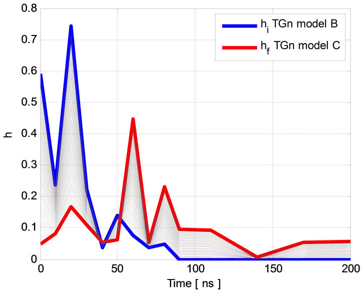
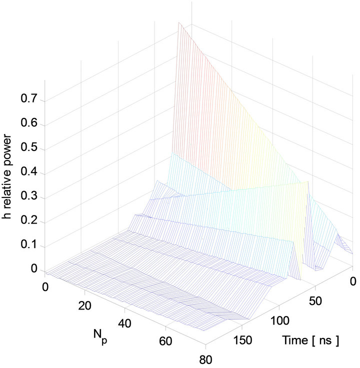
Figure 2. Switching between E1 and E2.
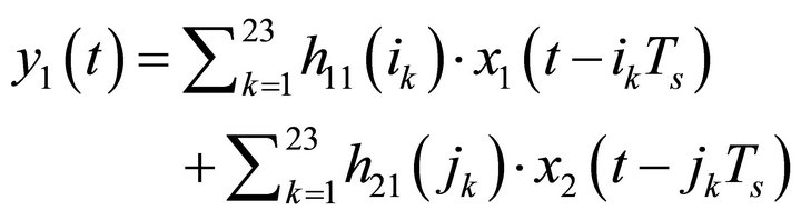
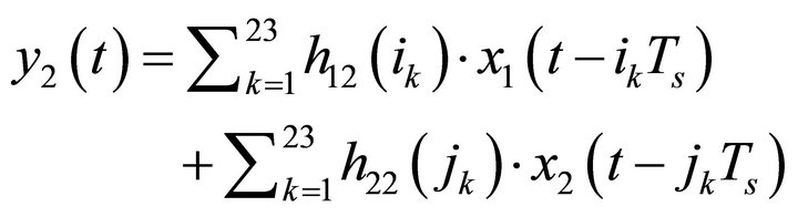
change of delays in architecture by connecting each multiplier block of the FIR by the corresponding shift Register block. Therefore, the number of multipliers in the FIR filters is equal to the maximum number of taps between all channels of all environments. The switch from the last h11 in E2 to the first h11 in E3 needs 23 taps (Table 3). Therefore, 4 FIR filters with 23 multipliers each are considered. Figure 4 presents two SISO channels of the time domain architecture based on FIR 147 filter with 23 multipliers.
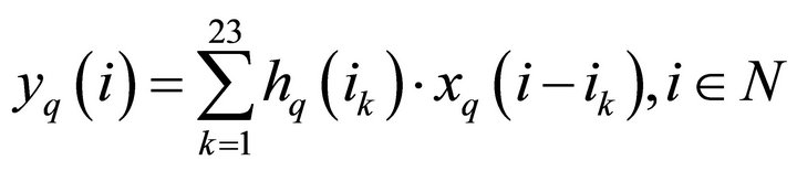
We have developed our own FIR filter instead of using Xilinx MAC FIR filter to make it possible to reload the FIR filter coefficients. The general formula for a FIR filter with 23 multipliers is:
 (17)
(17)
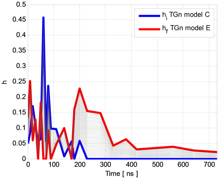
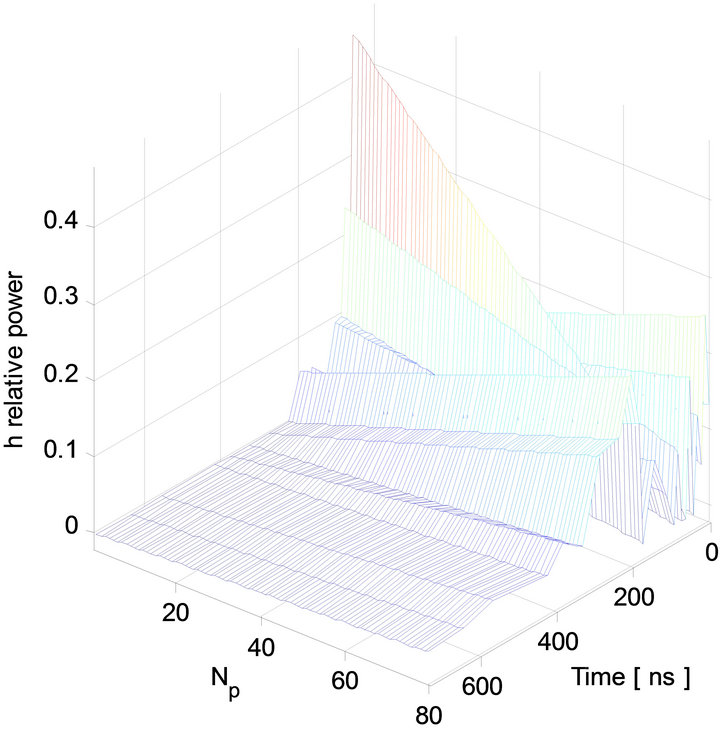
Figure 3. Switching between E2 and E3.
In this relation, the index q suggests the use of quantified samples and hq(ik) is the attenuation of the kth path with the delay ikTs.
The truncation block is located at the output of the final digital adder. It is necessary to reduce the number of bits to 14 bits. Thus, these samples can be accepted by the digital-to-analog converter (DAC), while maintaining the highest accuracy. The immediate solution is to keep the first 14 bits. It is a “brutal” truncation (B.T.). This truncation decreases the real value of the quantified output sample. Moreover, 36 − 14 = 22 bits will be eliminated. Thus, instead of an output sample y, we obtain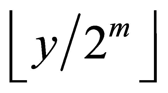 , where
  is the biggest integer number smaller or equal to u.
However, for low voltages, the brutal truncation generates zeros to the input of the DAC. Therefore, a better solution is the sliding truncation (S.T.) presented in Fig-
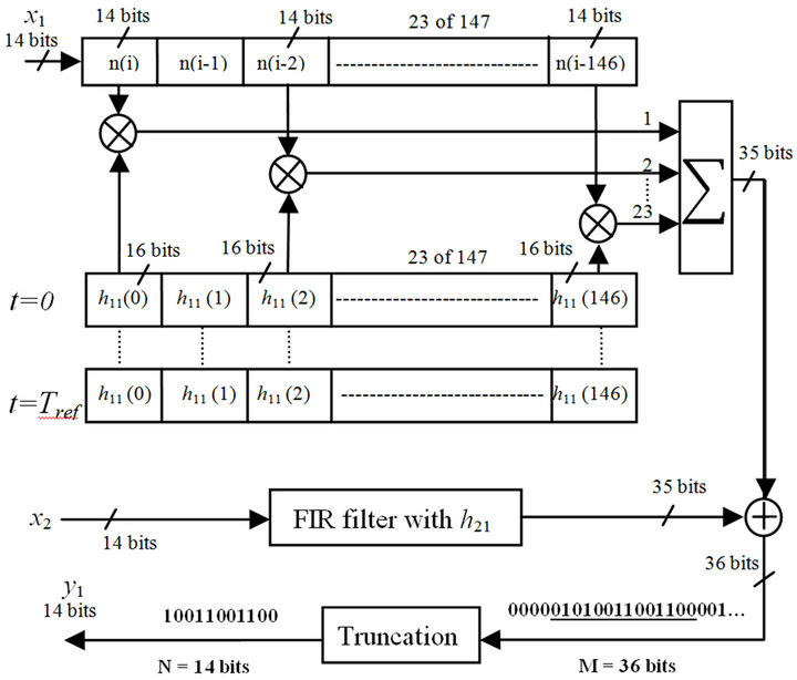
Figure 4. FIR 147 with 23 multipliers for one h11 and h21.
ure 4 which uses the 14 most significant bits. This solution modifies the output sample values. Therefore, the use of a reconfigurable amplifier after the DAC must be used to restore the correct output value. It must be divided by the corresponding sliding factor.
4.2. Implementation on FPGA Virtex-IV
The XtremeDSP Virtex-IV board from Xilinx [3] is used for the implementation. The XtremeDSP features dualchannel high performance ADCs (AD6645) and DACs (AD9772A) with 14-bit resolution, a user programmable Virtex-IV FPGA, programmable clocks, support for external clock, host interfacing PCI, two banks of ZBTSRAM, and JTAG interfaces. The simulations and synthesis are made with Xilinx ISE [3] and ModelSim software [26].
The 2 × 2 MIMO architectures are implemented in the FPGA Virtex-IV which has 2 ADC and 2 DAC, it can be connected to only 2 down-conversion and 2 up conversion RF units. To test a higher order MIMO array, the use of more performing FPGA as Virtex-VII [3] is recommended.
Table 4 presents the FPGA utilization of 2 × 2 MIMO time domain architecture using four FIR filters with their additional circuits used to dynamically reload the channel coefficients.
In the FPGA, the clock is controlled by a Virtex-II which is connected to the Virtex-IV.
4.3. Impulse Responses Transfer
The channel impulse responses are stored on the hard disk of the computer and read via the PCI bus and then stored in the FPGA dual-port RAM. Figure 5 shows the connection between the computer and the FPGA board to
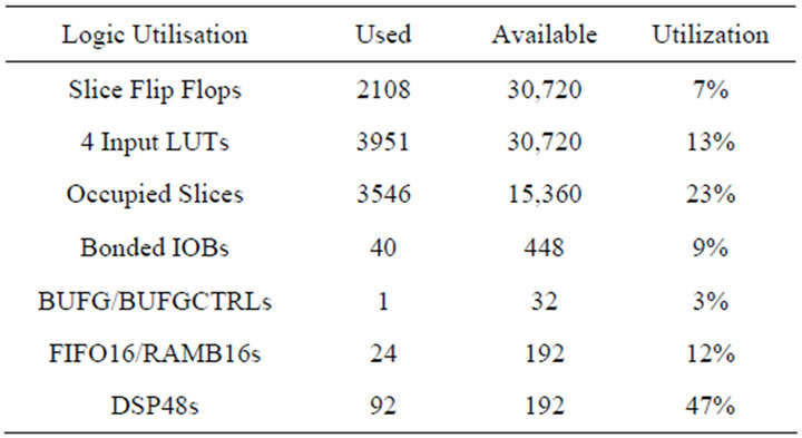
Table 4. Virtex-IV utilization summary for the 2 × 2 MIMO architecture.
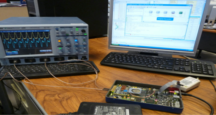
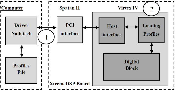
Figure 5. Connection between the computer and the XtremeDSP board.
reload the coefficients. The successive profiles are considered for the test of a 2 × 2 MIMO time-varying channel.
The maximum data transfer of the impulse responses is: 23 × 4 = 92 words of 16 bits = 184 bytes to transmit for a MIMO profile, which is: 184 × fref (Bps). fref depends on each environment in the scenario. For E1 it is 3.680 (kBps) and for E2 and E3 it is 7.360 (kBps).
The MIMO profiles are stored in a text file on the hard disk of a computer. This file is then read to load the memory block which will supply RAM blocks on the simulator (one block for each tap of the impulse response). Each block RAM has a memory of 64 (kB), thus 512 (kbits). The impulse responses are quantified on 16 bits, therefore, up to 32,000 MIMO profiles can be supplied in the RAM blocks. Each environment needs 4 blocks RAM for the power of the impulse responses and 4 blocks for the delays, which is a total of 8 blocks RAM. Reading the file can be done either from USB or PCI interfaces, both available on the used prototyping board. The PCI bus is chosen to load the profiles. It has a speed of 30 (MB/s). In addition, this is a bus of 32 (bits). Thus, on each clock pulse two samples of the impulse response are transmitted.
The Nallatech driver in Figure 5 provides an IP sent directly to the “Host Interface” that reads it from the PCI bus and stores these data in a FIFO memory. The module called “Loading profiles” reads and distributes the impulse responses in “RAM” blocks. While a MIMO profile is used, the following profile is loaded and will be used after the refresh period.
5. Accuracy
In order to determine the accuracy of the digital block, a comparison is made between the theoretical and the Xilinx output signals.
An input Gaussian signal x(t) is considered for the two inputs of the 2 × 2 MIMO simulator. The use of a Gaussian signal is preferred because it has a limited duration in time domain. To simplify the calculation, we consider x1(t) = x2(t):
 (18)
(18)
where Wt = 50·Ts, mx = 25·Ts and σ = 4·Ts (small enough to show the effect of each tap on the output signal).
The A/D and D/A converters of the development board have a full scale [−Vm, Vm], with Vm = 1 V. For the simulations we consider xm = Vm/2. The theoretic output signals are calculated by:
 (19)
(19)
 (20)
(20)
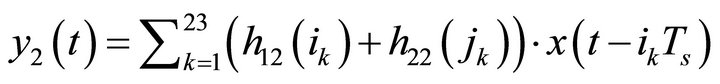
For x1(t) = x2(t):
 (21)
(21)
 (22)
(22)
and in this case, the occupation on FPGA is decreased if h11 and h21 (respectively h12 and h22) are summed before charging to the RAM blocks. In fact, two channels will be simulated instead of four. The number of RAM blocks and multipliers will be divided by 2. Thus, the occupation on FPGA of 4 × 4 MIMO channel (with the same input signals) is equal to the occupation of 2 × 2 MIMO channel (with different input signals).
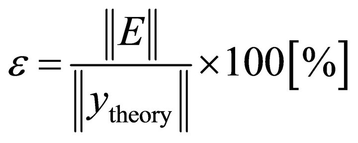
The relative error is given for each output sample by:
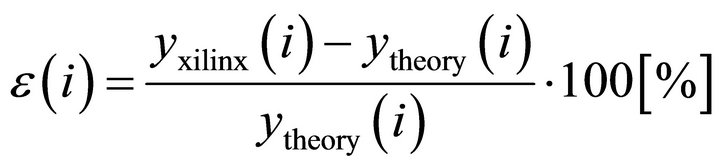 (23)
(23)
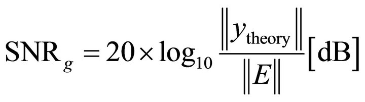
where yxilinx and ytheory are vectors containing the samples of corresponding signals and ytheory equal to y1 or y2. The Signal-to-Noise Ratio (SNR) is:
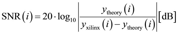 (24)
(24)
where 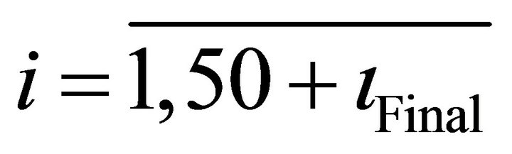 and
and  is the maximum number of the last tap between h11 and h21, or between h12 and h22.
Three snapshots of y1 in E1, E2 and E3 respectively with their SNR are presented in Figure 6.
For TGn channel model B (E1), the effect of the channel on the input signals is negligible. In fact, the length of the impulse responses is 14 (very low if we compare it to
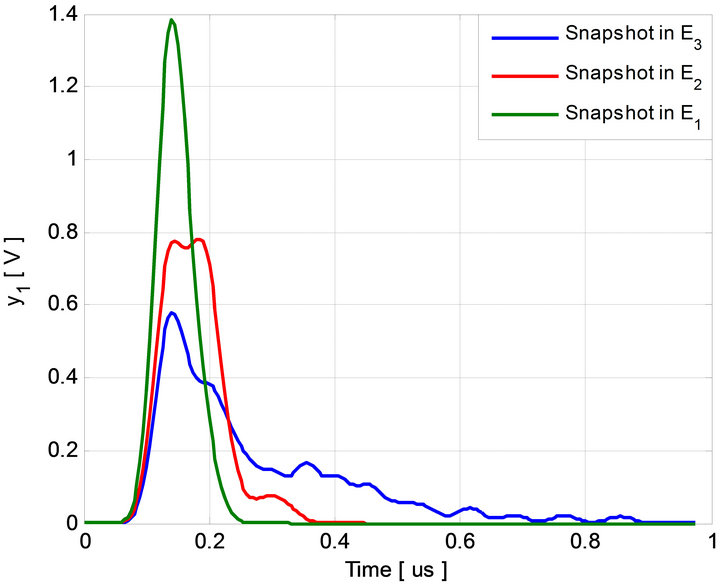
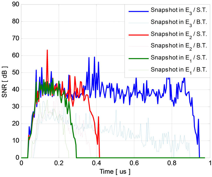
Figure 6. Three snapshots of y1 in E1, E2 and E3 respectively with their SNR.
the length of 6σ). However, TGn channel model C (E2) and E (E3), the maximum length of the impulse responses is high which will affect the input signals. As shown in Figure 6, the SNR is low for small values of the output signal.
The global values of the relative error and of the SNR computed for the output signal before and after the final truncations are necessary to evaluate the accuracy of the architecture. The global relative error is computed by:
 (25)
(25)
The global SNR is computed by:
 (26)
(26)
where E = yXilinx − ytheory is the error vector.
For a given vector , its Euclidean norm ||x|| is:
 (27)
(27)
Table 5 shows the mean global values of the SNR between the Xilinx output signal and the theoretical output signal using 2 × 2 MIMO time domain architecture for all the profiles in each environment. The results are given with brutal truncation and with sliding truncation. It has been shown that the sliding truncation increases the SNR about 30 to 40 (dB).
6. Conclusions
In this paper, specific architecture of the digital block of the simulator is presented to characterize a scenario indoor to outdoor using TGn channel models. An algorithm has been proposed and tested to switch between the environments in a continuous manner. Also, to decrease the number of multipliers on the FPGA and to switch from one environment to another, a solution is proposed to control the change of delays in architecture for timevarying channel. The impulse responses have been implemented in the digital block of the simulator.
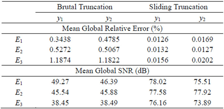
Table 5. The mean global relative error and SNR.
The time domain architecture used for the design of the digital block represents the best solution, especially for MIMO systems. In fact, it occupies just 23% of slices on the FPGA Virtex-IV. Also, it has a small latency of 125 (ns).
Moreover, a study of the architecture accuracy for time-varying 2 × 2 MIMO channel has been presented. It showed that the SNR increases of about 30 to 40 (dB) using a sliding truncation.
For our future work, simulations made using a VirtexVII [3] XC7V2000T platform will allow us to simulate up to 300 SISO channels. In parallel, measurement campaigns will be carried out with the MIMO channel sounder realized by IETR to obtain the impulse responses of the channel for various types of environments. The final objective of these measurements is to obtain realistic MIMO channel models in order to supply the hardware simulator. A graphical user interface will also be designed to allow the user to reconfigure the simulator parameters.
7. Acknowledgements
The authors would like to thank the “Région Bretagne” for its financial support of this work, which is a part of PALMYRE-II project.
REFERENCES
- S. Behbahani, R. Merched and A. Eltawil, “Optimizations of a MIMO Relay Network,” IEEE Transactions on Signal Processing, Vol. 56, No. 10, 2008, pp. 5062-5073. doi:10.1109/TSP.2008.929120
- A. Cetiner, E. Sengul, E. Akay and E. Ayanoglu, “A MIMO System with Multifunctional Reconfigurable Antennas,” IEEE Antennas and Wireless Propagation Letters, Vol. 5, No. 1, 2006, pp. 463-466. doi:10.1109/LAWP.2006.885171
- Xilinx, “FPGA, CPLD and EPP Solutions.” www.xilinx.com
- S. Picol, G. Zaharia, D. Houzet and G. El Zein, “Design of the Digital Block of a Hardware Simulator for MIMO Radio Channels,” IEEE PIMRC, Helsinki, 2006.
- V. Erceg, L. Shumacher, P. Kyritsi, et al., “TGn Channel Models,” IEEE 802.11-03/940r4, 10 May 2004.
- Agilent Technologies, “Advanced Design System—LTE Channel Model—R4-070872 3GPP TR 36.803 v0.3.0,” 2008.
- H. Farhat, R. Cosquer, G. Grunfelder, L. Le Coq and G. El Zein, “A Dual Band MIMO Channel Sounder at 2.2 and 3.5 GHz,” Instrumentation and Measurement Technology Conference Proceedings, Victoria, 12-15 May 2008.
- P. Almers, E. Bonek, et al., “Survery of Channel and Radio Propagation Models for Wireless MIMO Systems,” EURASIP Journal on Wireless Communications and Networking, 2007, Article ID 19070.
- J. Salz and J. H. Winters, “Effect of Fading Correlation on Adaptive Arrays in Digital Mobile Radio,” IEEE Transactions on Vehicular Technology, Vol. 43, No. 4, 1994, pp. 1049-1057.
- L. Schumacher, K. I. Pedersen and P. E. Mogensen, “From Antenna Spacings to Theoretical Capacities— Guidelines for Simulating MIMO Systems,” IEEE Proceedings of Personal Indoor and Mobile Radio Conference, Vol. 2, 2002, pp. 587-592.
- Spirent Communications, “Wireless Channel Emulator,” 2006.
- Rohde & Schwarz, “Baseband Fading Simulator ABFS, Reduced Costs through Baseband Simulation,” 1999.
- P. Murphy, F. Lou, A. Sabharwal and P. Frantz, “An FPGA Based Rapid Prototyping Platform for MIMO Systems,” Asilomar Conferences on Signals, Systems and Computers, Vol. 1, 2003, pp. 900-904.
- D. Umansky and M. Patzold, “Design of MeasurementBased Stochastic Wideband MIMO Channel Simulators,” IEEE Global Communications Conference, Honolulu, 30 November-4 December 2009.
- S. Fouladi Fard, A. Alimohammad, B. Cockburn and C. Schlegel, “A Single FPGA Filter-Based Multipath Fading Emulator,” IEEE Global Communications Conference, Honolulu, 30 November-4 December 2009.
- M. Al Mahdi Eshtawie and M. Bin Othma, “An Algorithm Proposed for FIR FILTER Coefficients Representation,” World Academy of Science, Engineering and Technology, 2007.
- H. Eslami, S. V. Tran and A. M. Eltawil, “Design and Implementation of a Scalable Channel Emulator for Wideband MIMO Systems,” IEEE Transactions on Vehicular Technology, Vol. 58, No. 9, 2009, pp. 4698-4708. doi:10.1109/TVT.2009.2027439
- B. Habib, G. Zaharia and G. El Zein, “MIMO Hardware Simulator: Digital Block Design for 802.11ac Applications with TGn Channel Model Test,” IEEE VTC Spring, Yokohama, 6-9 May 2012.
- B. Habib, G. Zaharia and G. El Zein, “Digital Block Design of MIMO Hardware Simulator for LTE Applications,” IEEE ICC, Ottawa, 10-15 June 2012.
- K. Borries, E. Anderson and P. Steenkiste, “NetworkScale Emulation of General Wireless Channels,” IEEE VTC Fall, San Francisco, 5-8 September 2011.
- A. Damnjanovic, et al., “A Survey on 3GPP Heterogeneous Networks,” IEEE Wireless Communications, Vancouver, 1-3 June 2011.
- W. C. Jakes, “Microwave Mobile Communications,” Wiley & Sons, New York, 1975.
- J. P. Kermoal, L. Schumacher, K. I. Pedersen, P. E. Mogensen and F. Frederiksen, “A Stochastic MIMO Radio Channel Model with Experimental Validation,” IEEE Journal on Selected Areas of Communications, Vol. 20, No. 6, 2002, pp. 1211-1226. doi:10.1109/JSAC.2002.801223
- Q. H. Spencer, et al., “Modeling the Statistical Time and Angle of Arrival Characteristics of an Indoor Environment,” IEEE Journal on Selected Areas of Communications, Vol. 18, No. 3, 2000, pp. 347-360. doi:10.1109/49.840194
- C.-C. Chong, D. I. Laurenson and S. McLaughlin, “Statistical Characterization of the 5.2 GHz Wideband Directional Indoor Propagation Channels with Clustering and Correlation Properties,” IEEE proceedings of Vehicular Technology Conference, Vol. 1, 2002, pp. 629-633.
- ModelSim, “Advanced Simulation and Debugging.” http://model.com