Circuits and Systems
Vol. 3 No. 2 (2012) , Article ID: 18550 , 5 pages DOI:10.4236/cs.2012.32027
Effect of Temperature & Supply Voltage Variation on Stability of 9T SRAM Cell at 45 nm Technology for Various Process Corners
1VLSI Group, Atal Bihari Vajpayee Indian Institute of Information Technology and Management, Gwalior, India
2Department of Electronics & Communications, Sir Padampat Singhania University, Udaipur, India
3Department of Electronics & Communications, Bipin Chandra Tripathi kumaon Engineering College, Dwarahat, India
Email: shilpibirla@gmail.com
Received February 8, 2012; revised March 7, 2012; accepted March 17, 2012
Keywords: DSM Technology; Process Corners; Write Margin; Read Current; Static Noise Margin
ABSTRACT
Due to the continuous rising demand of handheld devices like iPods, mobile, tablets; specific applications like biomedical applications like pacemakers, hearing aid machines and space applications which require stable digital systems with low power consumptions are required. As a main part in digital system the SRAM (Static Random Access Memory) should have low power consumption and stability. As we are continuously moving towards scaling for the last two decades the effect of this is process variations which have severe effect on stability, performance. Reducing the supply voltage to sub-threshold region, which helps in reducing the power consumption to an extent but side by side it raises the issue of the stability of the memory. Static Noise Margin of SRAM cell enforces great challenges to the sub threshold SRAM design. In this paper we have analyzed the cell stability of 9T SRAM Cell at various processes. The cell stability is checked at deep submicron (DSM) technology. In this paper we have analyzed the effect of temperature and supply voltage (Vdd) on the stability parameters of SRAM which is Static Noise Margin (SNM), Write Margin (WM) and Read Current. The effect has been observed at various process corners at 45 nm technology. The temperature has a significant effect on stability along with the Vdd. The Cell has been working efficiently at all process corners and has 50% more SNM from conventional 6T SRAM and 30% more WM from conventional 6T SRAM cell.
1. Introduction
With continuous scaling of the supply voltages, the SRAM cell does not function properly at sub-threshold supply voltage ranges as at theses voltages the SNM deteriorates and is not enough for reliable and stable operation. With the increased complexity of the microprocessors and digital signal processors on-chip register files and SRAMs are expected to increase significantly while maintaining the stability. SRAM caches represent an important part of modern processors as they have an increasingly large influence on the system speed and power consumption [1]. SRAMs are expected to increase significantly as the demands of handheld devices are increasing day by day but stability demand is rising.
Various SRAMs from 6T to 13T [2-5] has been proposed to improve the stability and performance along with low power consumption. In this paper we have analyzed the stability and leakage of our proposed SRAM PNN stack at various process corners. This cell is suitable and operational for deep sub-threshold technology and is operational at all the process corners. Process variation like dopant variation, temperature, and threshold affects the overall performance of the design at deep sub micron technology [6].
This paper is organized as follows: In Section 2 a brief overview is given about 6T SRAM cell, Section 3 deals with the proposed 9T SRAM cell whose analysis is to be done. Section 4 includes the Simulation & Analysis part and finally the conclusion.
2. Conventional 6T Sram Cell
In traditional 6T-SRAM as shown in Figure 1, it has one wordline and two bitlines which are required during a read and write operations. The cell must be both stable during a read event and writeable during a write event ignoring redundancy; such functionality must be preserved for each cell under worst-case variation. At the cell level, transistor strength ratios must be chosen such that cell static noise margin and write margin are both maintained, which presents conflicting constraints on the cell transistor strengths.
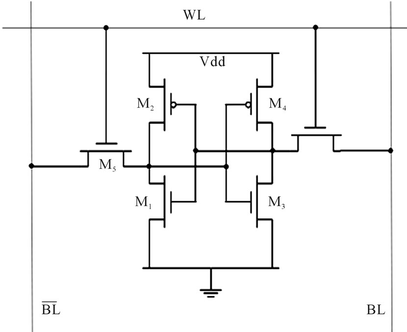
Figure 1. 6T SRAM cell.
For cell stability during a read, it is desirable to strengthen the storage inverters and weaken the pass-gates. The opposite is desired for cell write ability a weak storage inverter and strong pass-gates. This delicate balance of transistor strength ratios can be severely impacted by device variation, which dramatically degrades stability and write margins, especially in scaled technologies. Low supply voltages further exacerbate the problem as threshold voltage variation consumes a larger fraction of these voltage margins. Variability can thus limit the minimum operating voltage of SRAM.
3. 9T SRAM Cell-Working
The 9T SRAM cell is shown in Figure 2. This cell has 9T and it is like the conventional SRAM cell which has cross coupled inverters like the conventional cell. It is connected in PNN fashion that is one PMOS as Pull-up transistor and 2 NMOS one is for stacking purpose and the other Pull-down transistor. It has one discharging NMOS transistor ND. The RD signal is always connected to ground reference during the read operation. The data storage in the 9T cell is performed by the crosscouple inverters [7]. Two NMOS access transistors (PG) NA1 and NA2 connect to the virtual storage nodes (V1 & V2) to the write bitline pair when the write wordline (WDL) is on. N1 and N2 transistors are placed in between the pull-up PMOS transistors P1 and P2 and the pull-down NMOS transistors N3 and N4 of the crosscoupled inverters. RDL is read signal which controls the read port. N3 and N4 are the pull down transistors. During read the RDL signal is grounded so that there will be less power consumption. There is only one wordline for reading and writing. During write “1” keep BL as high and also WDL and RDL high. Similarly during write “0” we can keep BL as “0”. During read keep WDL and RDL as “0”.
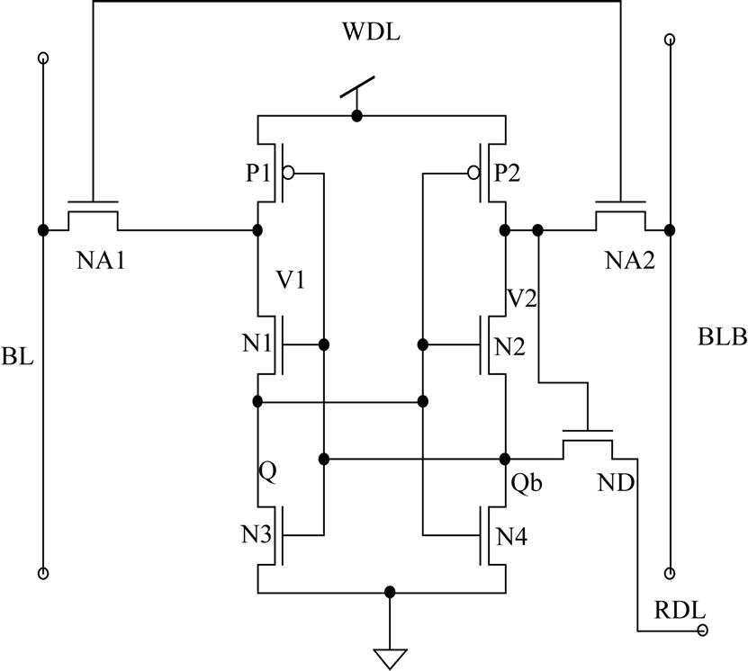
Figure 2. 9T SRAM cell.
4. Analysis of the Stablity of the Cell
In order to verify the robustness of an integrated circuit design, semiconductor manufacturers will fabricate corner lots, which are groups of wafers that have had process parameters adjusted according to these extremes, and will then test the devices made from these special wafers at varying increments of environmental conditions, such as voltage, clock frequency, and temperature, applied in combination (two or sometimes all three together) in a process called characterization. Corner-lot analysis is most effective in digital electronics because of the direct effect of process variations on the speed of transistor switching during transitions from one logic state to another, which is not relevant for analog circuits, such as amplifiers.
The stability of any SRAM cell is basically measure from the noise margin, write margin and read current of the cell [8]. We have analyzed the three parameters of stability at various process corners along with the temperature variation and voltage variations. We have mainly focused on three process variations which are of more concerned for digital applications. We have simulated the SRAM cell at 45 nm technology taking Vtn = 0.22 V and Vtp = |0.22| V.
4.1. Noise Margin Analysis
The Static Noise Margin (SNM) is the maximum amount of noise voltage that can be tolerated at the both inputs of the cross-coupled inverters in different directions while inverters still maintain bi-stable operating points and cell retains its data [8-10]. In other words, the Static Noise Margin (SNM) quantifies the amount of noise voltage required at the storage nodes of SRAM to flip the cell data. We have varied the temperature from –20˚C to 125˚C and the Vdd has been varied from 0.5 V to 1.0 V. Reducing the Vdd will reduce the SNMAs the temperature is increased the SNM reduces in the three corners (TT, FF, FS) as shown in Figures 3-5 respectively.
The highest SNM is 0.3949 V at 1.0 Vdd and at TT corner, for FF corner the highest SNM is 0.3649 V at 1.0 Vdd, and for FS corner the highest SNM is 0.3749 V at 1.0 Vdd. But the highest SNM is calculated at the lowest temperature. We have taken the temperature 50˚C and varying Vdd and find the SNM which is given in Table 1.
4.2. Write Margin Analysis
Write Margin is an important parameter which ensures robust write operation. The Write Margin (WRM) is defined as the potential difference between the BL level at which the data is flipped and the end-point (e.g., GND). The effect of temperature and voltage variation is also analyzed for write margin. We have varied the temperature from –20˚C to 125˚C and the Vdd has been varied from 0.5 V to 1.0 V. The write margin increases exponentially with Vdd and also incraeses as temperature incareses as shown in Figures 6-8.
The highest WM is 0.4859 V at 1.0 Vdd and at FS corner, for FF corner the highest WM is 0.4379 V at 1.0 Vdd, and for TT corner the highest SNM is 0.3771 V at 1.0 Vdd. But the highest SNM is calculated at the highest temperature and highest Vdd. We have taken the tem-
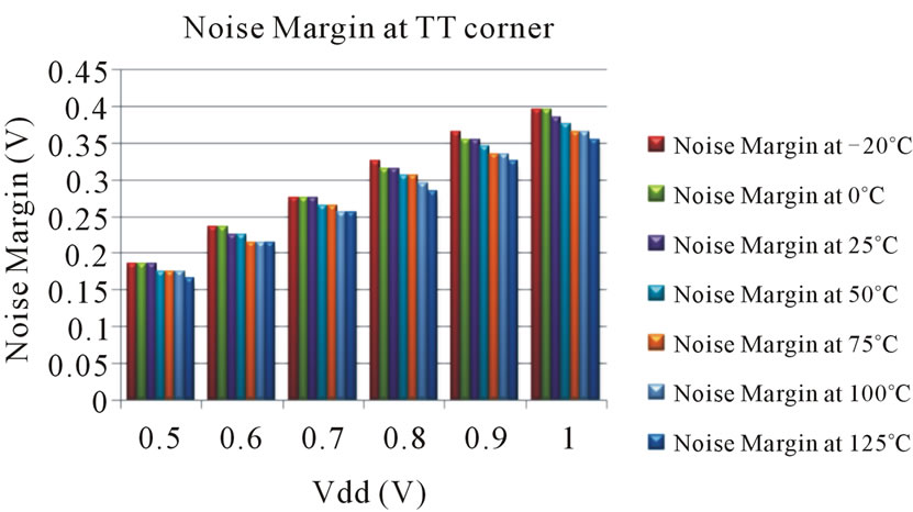
Figure 3. Noise margin at TT corner with respect to temperature variation.
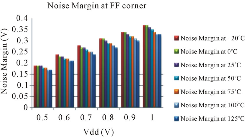
Figure 4. Noise margin at FF corner with respect to temperature variation.
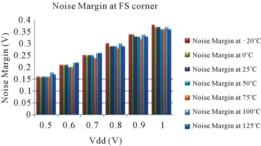
Figure 5. Noise margin at FS corner with respect to temperature variation.
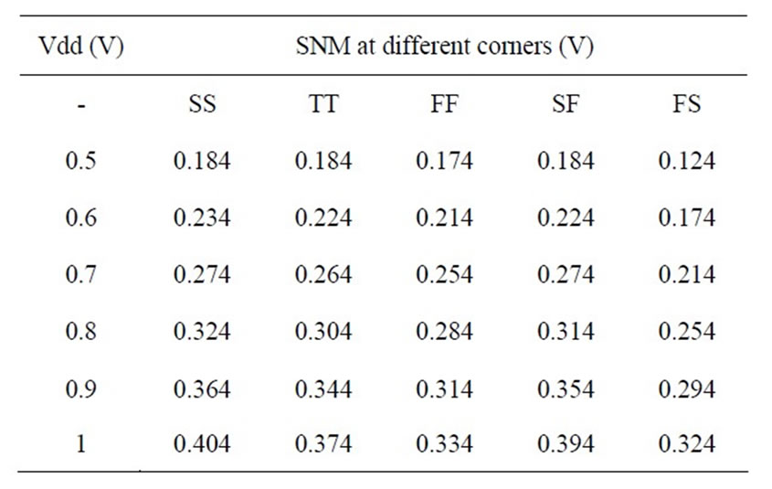
Table 1. SNM at different process corners.
perature 50˚C and varying Vdd and find the WM which is given in Table 2.
4.3. Read Current Analysis
The read current in an SRAM memory cell is the current flowing from the precharged bit line (BL) along the conducting pass-gate (PG) transistor and the pull-down (PD) transistor to ground. We have varied the temperature from –20˚C to 125˚C and the Vdd has been varied from 0.5 V to 1.0 V. The read current decreases drastically with Vdd decreases and the effect of temperature is not very prominent as in Figures 9-11.
The highest read current is 31.6 µA at 1.0 Vdd and at FF corner, for FS corner the highest read current is 29.8 µA at 1.0 Vdd, and for TT corner the highest SNM is 23 µA at 1.0 Vdd. But the highest read current is calculated at the lower temperature and highest Vdd. We have taken the temperature 50˚C and varying Vdd and find the read current which is given in Table 3.
5. Conclusion
In this paper we have anlaysed the stability parameters at various process corners to find the work ability of the cell and it has been successfully operative in all the process corners. It has been observed that cell is stable
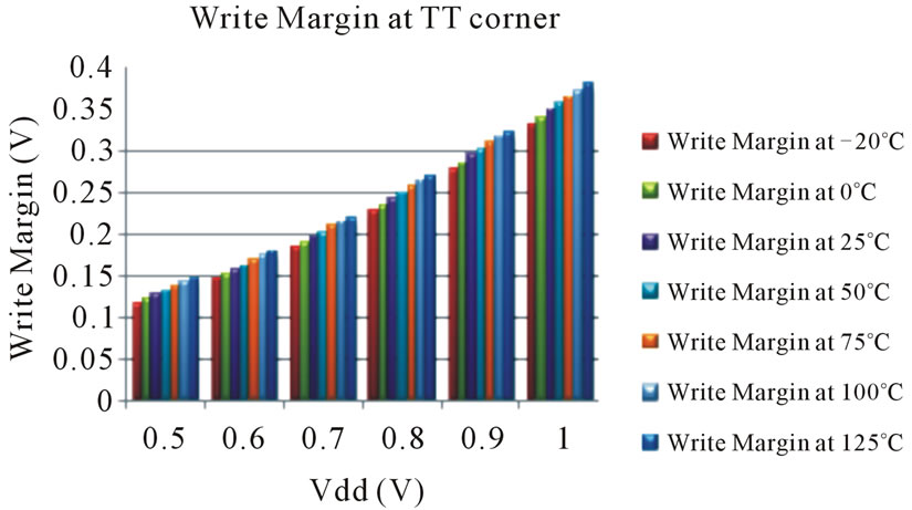
Figure 6. Write margin at TT corner with respect to temperature variation.
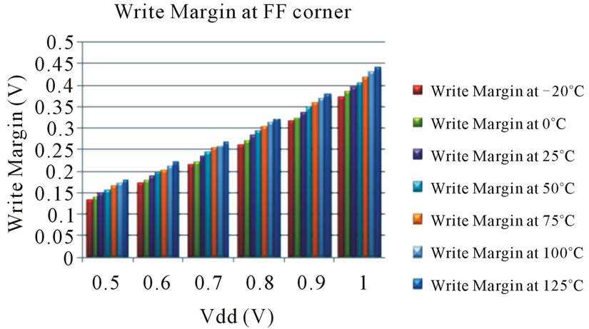
Figure 7. Write margin at FF corner with respect to temperature variation.
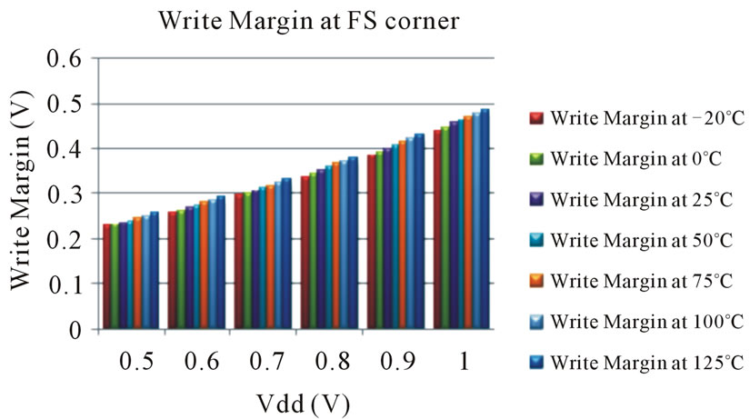
Figure 8. Write margin at FS corner with respect to temperature variation.
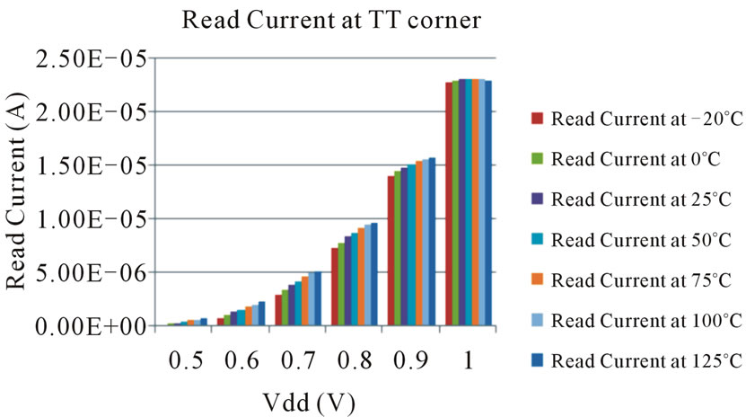
Figure 9. Read current at TT corner with respect to temperature variation.
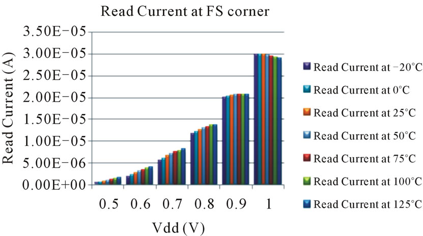
Figure 10. Read current at FS corner with respect to temperature variation.
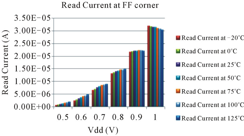
Figure 11. Read current at FF corner with respect to temperature variation.
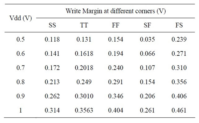
Table 2. Write Margin at different process corners.
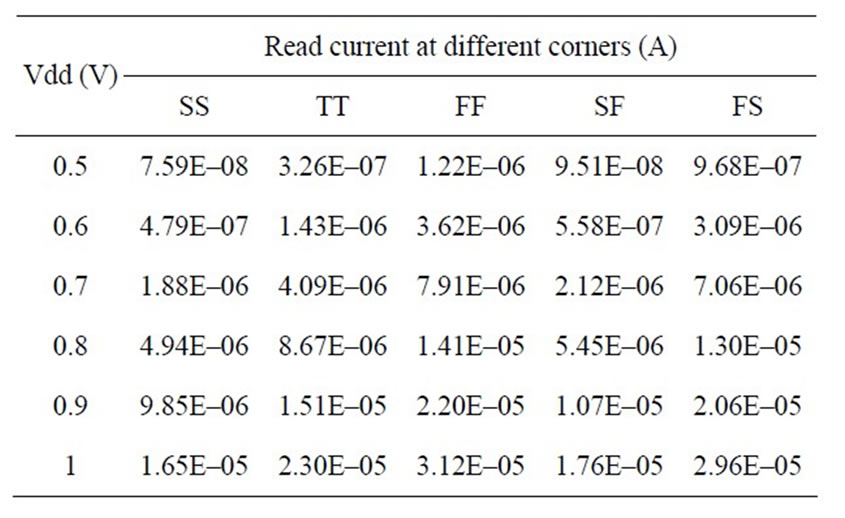
Table 3. Read current at different process corners.
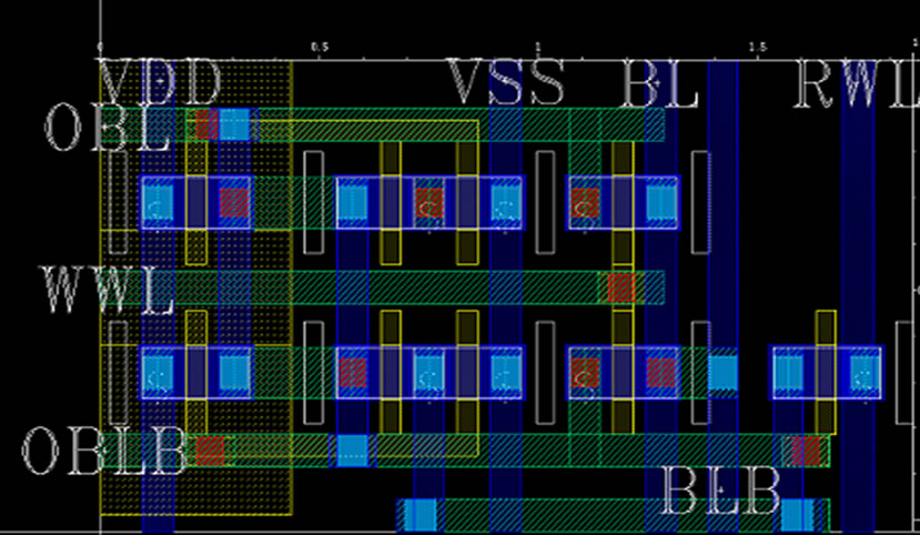
Figure 12. Layout of 9T SRAM cell.
with SNM at 0.8 V with 0.3 V which is higher by 50% from conventional 6T. The write ability of the cell at 0.8 V with temperature 50˚C is also higher by the conventional 6T SRAM by 30%. The cell is also having low leakge current as the leakage current measure at 0.8 V at FF corner is 43 nA and the leakage current in the worst case is 68 nA. The cell area is 1.901 µm2 which can be further optimized by sizing the cell. The cell layout is as shown in Figure 12. The cell is suitable for applications where stability and power are concerned.
6. Acknowledgements
The authors are grateful to their respective organizations for their encouragement and support.
REFERENCES
- B. H. Calhoun and A. P. Chandrakasan, “Static Noise Margin Variation for Sub-Threshold SRAM in 65 nm CMOS,” IEEE Journal of Solid-State Circuits, Vol. 41, No. 7, 2006, pp. 1673-1679.
- M. Sinangil, N. Verma and A. P. Chandrakasan, “A Reconfigurable 8T Ultra-Dynamic Voltage Scalable (U-DVS) SRAM in 65 nm CMOS,” IEEE Journal of Solid-State Circuits, Vol. 44, No. 11, 2009, pp. 3163-3173.
- Z. Y. Liu and V. Kursun, “Characterization of a Novel Nine-Transistor SRAM Cell,” IEEE Transaction of Very Large Scale Integration Systems, Vol. 16, No. 4, 2008, pp. 488-492.
- S. Lin, Y.-B. Kim and F. Lombardi, “Design and Analysis of a 32 nm PVT Tolerant CMOS SRAM Cell for Low Leakage and High Stability,” Integration the VLSI Journal, Vol. 43, No. 2, 2010, pp. 176-187. doi:10.1016/j.vlsi.2010.01.003
- A. J. Bhavnagarwala, X. Tang and J. D. Meindl, “The Impact of Intrinsic Device Fluctuations on CMOS SRAM Cell Stability,” IEEE Journal of Solid-State Circuits, Vol. 36, No. 4, 2001, pp. 658-665. doi:10.1109/4.913744
- Z. Guo, A. Carlson, L.-T. Pang, K. Duong, T.-J. K. Liu and B. Nikolic, “Large-Scale Read/Write Margin Measurement in 45 nm CMOS SRAM Arrays,” IEEE Symposium on VLSI Circuits Digest of Technical Papers, Honolulu, 18-20 June 2008, pp. 42-43.
- R. K. Singh, S. Birla and M. Pattanaik, “Characterization of PNN Stack SRAM Cell at Deep Sub-Micron Technology with High Stability and Low Leakage for Multimedia Applications,” International Journal of Computer Applications, Vol. 33, No. 1, 2011, pp. 13-17. doi:10.5120/3409-4756
- J. J. Wang, S. Nalam and B. H. Calhoun, “Analyzing Static and Dynamic Write Margin for Nanometer SRAMs,” International Symposium on Low Power Electronics and Design, Bangalore, 11-13 August 2008, pp. 129-134.
- E. Seevinck, et al., “Static-Noise Margin Analysis of MOS SRAM Cells,” IEEE Journal of Solid-State Circuits, Vol. 22, No. 5, 1987, pp. 748-754. doi:10.1109/JSSC.1987.1052809
- S. Birla, M. Pattanaik and R. K. Singh, “Static Noise Margin Analysis of Various SRAM Topologies,” IACSIT International Journal of Engineering and Technology, Vol. 3, No. 3, 2011, pp. 304-309.