Journal of Modern Physics
Vol.2 No.11(2011), Article ID:8637,7 pages DOI:10.4236/jmp.2011.211164
Temperature and Doping Dependencies of the Transport Properties within GaN and GaAs
Department of Physics, Faculty of Girls, Ain Shams University, Cairo, Egypt
E-mail: afnan_Zakaria_000@yahoo.com
Received July 4, 2011; revised August 23, 2011; accepted September 9, 2011
Keywords: Monte Carlo, Steady State, Temperature Dependence, Doping Dependence
ABSTRACT
Temperature and doping dependencies of the transport properties have been calculated using an ensemble Monte Carlo simulation. We consider the polar optical phonon, acoustic phonons, piezoelectric, intervalley scatterings and Charged impurity scattering model of Ridley; furthermore, a non nonparabolic three-valley model is used. Our simulation results have shown that the electron velocity in GaN is less sensitive to changes in temperature than that associated with GaAs. Also it is found that GaN exhibits high peak drift velocity at room temperature, 2.8 × 10⁵ m/s, at doping concentration of 1 × 10²⁰ m–3 and the electron drift velocity relaxes to the saturation value of 1.3 × 10⁵ m/s which is much larger than that of GaAs. The weakening of the phonon emission rate at low temperature explains the extremely high low field mobility. Our results suggest that the transport characteristics of GaN are superior to that of GaAs, over a wide range of temperatures, from 100 K to 700 K, and doping concentrations, up to 1 × 1025 m–3.
1. Introduction
As the need for high speed electronics and optoelectronic growth, the study of electronic transport in semiconductor devices will play an important role in the development of microelectronics science and technology. Interest in GaN-based devices has risen rapidly [1-3]. There has been considerable interest in GaN due to its wide band gap and favorable material properties, such as high electron mobility and very high thermal conductivity. The large band gap energy of the III-nitrides insures that the breakdown electric field strength of these materials is much larger than that of GaAs [4].
The favorable electron transport characteristics of the III-V nitride semiconductor, GaN, have long been recognized. In 1975, Littlejohn et al. [5] were the first to report results obtained from semi-classical Monte Carlo simulations of the steady-state electron transport within bulk wurtzite GaN. A one-valley model for the conduction band was adopted in their analysis. The primary focus of their investigation was the determination of the velocity-field characteristic associated with GaN. The electron drift velocity achieving a maximum of about 2 × 10⁵ m/s at an applied electric field strength of about 100 × 105 V/m, with further increases in the applied electric field strength resulting in a slight decrease in the corresponding electron drift velocity.
In 1993, Gelmont et al. [2] reported on ensemble semi-classical two-valley Monte Carlo simulations of the electron transport within bulk wurtzite GaN, this analysis improving upon the analysis of Littlejohn et al. [5] by incorporating intervalley scattering into the simulations. They found that the negative differential mobility found in bulk wurtzite GaN is much more pronounced than that found by Littlejohn et al. [5], and that intervalley transitions are responsible for this. For a doping concentration of 1023 m–3, Gelmont et al. [2] demonstrated that the electron drift velocity achieves a peak value of about 2.8 × 10⁵ m/s at an applied electric field of about 140 × 105 V/m. The impact of intervalley transitions on the electron distribution function was also determined and shown to be significant. The impact of doping and compensation on the velocity-field characteristic associated with bulk wurtzite GaN was also examined. Since these pioneering investigations, ensemble Monte Carlo simulations of the electron transport within GaN have been performed numerous times.
In 1995, Mansour et al. [6] reported the use of such an approach in order to determine how the crystal temperature influences the velocity-field characteristic associated with bulk wurtzite GaN. Later that year, Kolník et al. [7] reported on employing full-band Monte Carlo simulations of the electron transport within bulk wurtzite GaN and bulk zincblende GaN, finding that bulk zincblende GaN exhibits a much higher low-field electron drift mobility than bulk wurtzite GaN. The peak electron drift velocity corresponding to bulk zincblende GaN was found to be only marginally greater than that exhibited by bulk wurtzite GaN.
In 1997, Bhapkar and Shur [8] reported on employing ensemble semi-classical three-valley Monte Carlos simulations of the electron transport within bulk and confined wurtzite GaN. Their simulations demonstrated that the two-dimensional electron gas within a confined wurtzite GaN structure will exhibit higher low-field electron drift mobility than bulk wurtzite GaN, by almost an order of magnitude.
In 1998, Albrecht et al. [9] reported on employing ensemble semi-classical five-valley Monte Carlo simulations of the electron transport within bulk wurtzite GaN, with the aim of determining elementary analytical expressions for a number of electron transport parameters corresponding to bulk wurtzite GaN. The subsequent ensemble full-band Monte Carlo simulations of Bellotti et al. [10], reported in 1999, produced results similar to those of O’Leary et al. [11]. The first known study of transient electron transport within the III-V nitride semiconductors was that carried by Foutz et al. [12], reported in 1997.
A more general analysis, in which transient electron transport within GaN, AlN, and InN was studied, was performed by Foutz et al. [13], and reported in 1999. As with their previous study, Foutz et al. [13] determined how electrons, initially in thermal equilibrium, respond to the sudden application of a constant electric field. In addition to Monte Carlo simulations of the electron transport within these materials, a number of other types of electron transport studies have been performed. In 1975, for example, Ferry [14] reported on the determination of the velocity-field characteristic associated with wurtzite GaN using a displaced Maxwellian distribution function approach.
On the experimental front, in 2000 Wraback et al. [15] reported on the use of a femtosecond optically detected time-of-flight experimental technique in order to experimentally determine the velocity-field characteristic associated with bulk wurtzite GaN. Wraback et al. [15] suggested that the large defect density characteristic of the GaN samples they employed, which were not taken into account in Monte Carlo simulations of the electron transport within this material, accounts for the difference between this experimental result and that obtained using simulation. They also suggested that decreasing the intervalley energy separation from about 2 eV to 340 meV, as suggested by the experimental results of Brazel et al. [16]. Review analyses of the electron transport within the III-V nitride semiconductors GaN, AlN, InN and GaAs have been reported by focused on the electron transport within the previous materials [3].
In this work, a comparison between the temperature dependence of the transport properties associated with GaN and GaAs, as determined on the basis of ensemble Monte Carlo calculations [17-19], will be presented for low impurity concentration less than 1 × 10²⁰ m–3. The velocity-field characteristics will be presented for the doping dependence. All donors were assumed to be ionized, and the free electron concentration was taken to be equal to the doping concentration.
Charged impurity model of Ridley [18,20,21] has been used in our study, which becomes convenient to use in the Monte Carlo method [22], since it solves the problem of cutting the impurity scattering at very small electron energy in the Brooks and Herring [23] model, at the same time it reconciles the different proposed [23,24] models used before in most previous transport investigations.
We simulate 5000 electrons and the main types of scattering mechanisms included in our calculations are, polar optical phonon scattering, acoustic phonon scattering, piezoelectric phonon scattering, equivalent intervalley phonon scattering, non-equivalent intervalley phonon scattering and Charged impurity scattering model of Ridley.
2. Three Band Structure
The electron energy E could be found for a given wave vector k using Kane relation [18,19]:
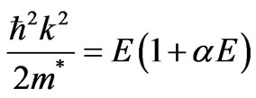 (1)
(1)
where α is the nonparabolicity coefficient and is given by
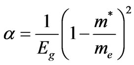 (2)
(2)
where me and Eg denote the free electron mass and the energy gap, respectively.
Nonparabolicity is considered in all valleys. The band structure and material parameters necessary for calculating the scattering probabilities used in our simulation are given in Table 1. These parameter selections are from S. K. O’Leary et al. [3] and M. A. Littlejohn [25] for GaN and GaAs respectively. The GaN parameters were originally from Foutz et al. [13] and Lambrecht and Segall [26].

Table 1. Material parameter selections for GaN and GaAs.
3. Monte Carlo Model [3,17,19]
The Monte Carlo method makes the solution of Boltzmann transport equation possible by the use of a statistical numerical approach. This approach follows the transport history of one or more carriers which are subject to the action of external forces. These forces which affect the particles consist of an applied field and scattering mechanisms. The Monte Carlo technique generates sequences of random numbers with specified distribution probabilities. These probabilities are used to describe quantities such as scattering events which determine the time between successive collisions of carriers.
The Monte Carlo simulation requires a detailed definition of the physical system as a starting point. The electron transport in a semiconductor requires material parameters, knowledge of energy band structure, lattice temperature and a definition of the applied electric field. The process of simulating the electron motion involves a number of computational steps to calculate the duration of each free flight, select the scattering mechanisms at the end of the flight and determine the final wave vector of the scattered electron.
4. Charged Ionized Impurity Scattering Rate
There are two famous approaches used to handle the charged impurity scattering problem [23,24], the scattering rate of electron by charged ionized donor may be calculated according to Brooks and Herring (B.H.) model [23]. Although the ionized impurity scattering is not important at high electron energy and so the nonparabolicity of the bands, we have included the nonparabolicity of the bands resulting in
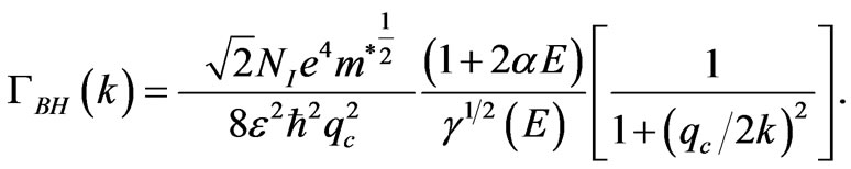 (3)
(3)
where  is the density of impurity atoms, while
is the inverse screening length defined by N is the electron concentration and
  is the electron temperature.
Also, Ridley [18,20,21] proposed a model; it reconciles the different proposed models used before.
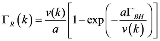 (4)
(4)
 ,
,  represent the Ridley [24] and the Brooks Herring [23] impurity scattering rates respectively,
  is the electron group velocity and a is the average distance apart the impurity center which is given by [18,21]
 (5)
(5)
5. Results and Discussion
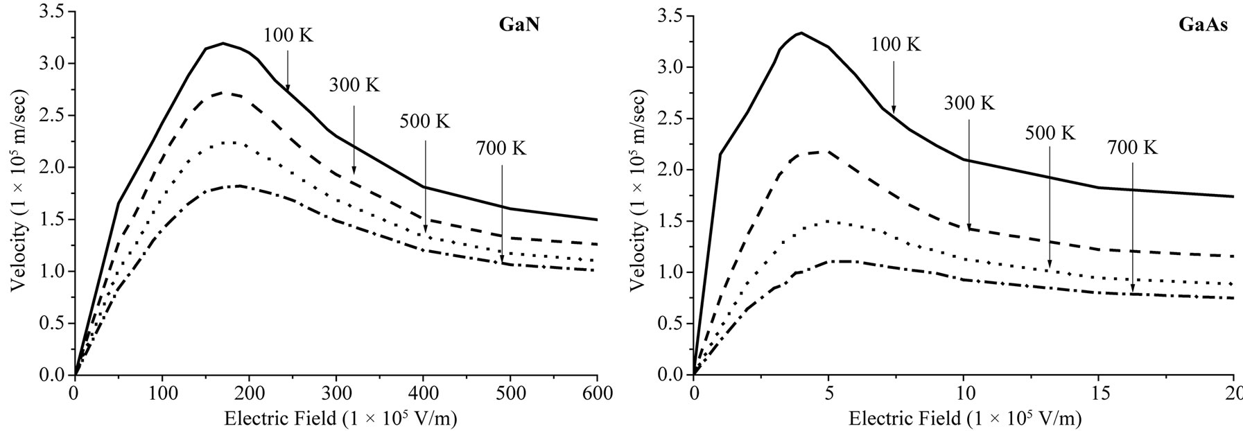
Electron drift velocity as a function of electric field is important in determining the performance of high-speed and microwave semiconductor devices. Here we show the results of temperature dependence of the steady-state velocity-field characteristics in GaN and GaAs. Figure 1(a) shows the velocity-field characteristics of GaN for temperatures ranging from 100 K to 700 K, for low impurity concentration less than 1 × 10²⁰ m–3. It is seen from the figure that the peak velocity and low-field mobility rise as the temperature falls, a consequence of the lower phonon occupation number

where ħwpo is the optical phonon energy, T is the lattice temperature, and kB is a Boltzmann’s constant, additionally, the small phonon occupation number lowers phonon scattering rates. The term (Npo + 1) represents phonons emission, while Npo represents phonons absorption. So the phonon absorption is absent at 100 K and high lowfield mobility is achieved, while the probability of phonon emission for a given process is zero unless the electron energy at least equals the energy of one phonon.
It can be seen that the peak drift velocity decreases and moves to higher electric field as the temperature is increased. Quantitatively, the peak drift velocity decreases from about 3.19 × 10⁵ m/s at 100 K to about 1.82 × 10⁵ m/s at 700 K in GaN. This is due to the general increase of total scattering rate with temperature. Monte Carlo simulations of the electron transport within GaAs have also been performed under the same conditions as GaN. Figure 1(b) shows the results of these simulations. Note that the electron drift velocity for the case of GaN is less sensitive to changes in temperature than that associated with GaAs and the peak drift velocities, in response to increases in the crystal temperature, do not drop as much in GaN as they do in GaAs. It is clear that GaN suitable for high speed device applications.
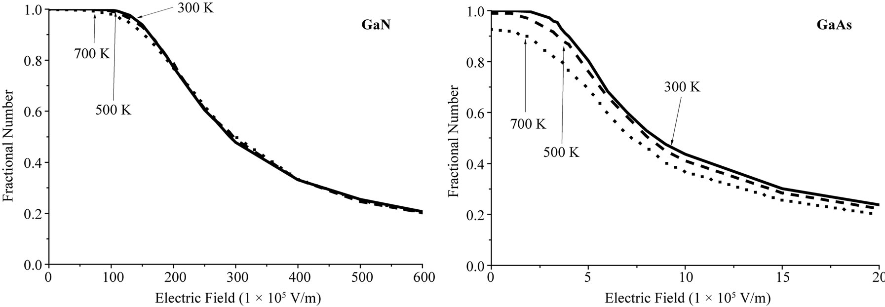
A comparison of the electron energy as a function of the applied electric field for various crystal temperatures in both GaN and GaAs is shown in Figure 2, for low impurity concentration less than 1 × 10²⁰ m–3. The total energy decreases as the temperature falls due to small phonon absorption rates at low temperature, so the fractional number of electrons in the Γ valley at low temperature is high as shown in Figure 3. In this figure the fractional number of electrons in Γ valley for various crystal temperatures in both GaN and GaAs has been calculated, for low impurity concentration less than 1 × 10²⁰ m–3.
In the case of GaN, the upper valleys begin to become occupied at roughly the same applied electric field strength independent of temperature. For the case of GaAs, however, the upper valleys are at a much lower energy than those in GaN. As the upper conduction band valleys are so close to the bottom of the conduction band for the case of GaAs , the thermal energy (at 700 K, kBT » 0.06 eV) is enough in order to allow a small fraction of the electrons to be transferred into the upper valleys even before an electric field is applied. When electrons occupy the upper valleys, intervalley scattering and the upper valleys larger effective masses reduce the overall electron drift velocity. This is another reason why the velocity-field characteristic associated with GaAs is more sensitive to variations in crystal temperature than that associated with GaN. Our results are in a good agreement with those given in Refs. [3,8].
One parameter that can be readily controlled during the fabrication of semiconductor devices is the doping concentration. Figure 4 shows how the velocity-field characteristic associated with GaN and GaAs change with doping concentration at 300 K. In the case of GaAs, the electron drift velocities decrease much more with increased doping than those associated with GaN and the peak in the velocity-field characteristic disappears completely for high doping concentrations. GaN maintains a higher electron drift velocity with increased doping levels than GaAs.
6. Conclusions
Electron transport at different temperatures in GaN and GaAs has been simulated using an ensemble Monte Carlo method. The peak velocity and low-field mobility, in both materials, rises as the temperature falls, a consequence of the lower phonon occupation number and lower phonon absorption scattering rate. The electron drift velocity decreases with increasing electric field at all temperatures over the entire field range investigated.
 (a) (b)
Figure 1. A comparison of the temperature dependence of the velocity-field characteristics associated with (a) GaN and (b) GaAs.
 (a) (b)
Figure 2. A comparison of the average electron energy as a function of the applied electric field at various crystal temperatures, for the cases of (a) GaN and (b) GaAs.
 (a) (b)
Figure 3. A comparison of the fractional electron number in the lowest energy valley of the conduction band, the Γ valley, as a function of the applied electric field at various crystal temperatures, for the cases of (a) GaN and (b) GaAs.
 (a) (b)
Figure 4. A comparison of the doping dependence of the velocity-field characteristics associated with (a) GaN and (b) GaAs at room temperatures.
The weakening of the phonon emission rate at low temperature explains the extremely high low field mobility. The total energy decreases as the temperature falls due to small phonon absorption rates at low temperature, so the fractional number of electrons in the Γ valley at low temperature is high. The transport properties of GaN were shown to be relatively insensitive to variations in temperature and doping concentration, unlike GaAs. So GaN is attractive for high power and high temperature electronic applications.
REFERENCES
- S. N. Mohammed and H. Morkoc, “Progress and Prospects of Group-III Nitride Semiconductors,” Progress in Quantum Electronics, Vol. 20, No. 5-6, 1996, pp. 361- 525. doi:10.1016/S0079-6727(96)00002-X
- B. Gelmont, K. Kim and M. Shur, “Monte Carlo Simulation of Electron Transport in Gallium Nitride,” Journal of Applied Physics, Vol. 74, No. 3, 1993, pp. 1818-1821. doi:10.1063/1.354787
- S. K. O’Leary, B. E. Foutz, M. S. Shur and L. F. Eastman, “Steady-State and Transient Electron Transport within the III-V Nitride Semiconductors, GaN, AlN, and InN: A Review,” Journal of Material Science: Materials in Electronics, Vol. 17, No. 2, 2006, pp. 87-126. doi:10.1007/s10854-006-5624-2
- S. Adachi, “GaAs and Related Materials, Bulk semiconducting and Superlattice Properties,” World Scientific, Singapore, 1994. doi:10.1142/9789812705709
- M. A. Littlejohn, J. R. Hauser and T. H. Glisson, “Monte Carlo Calculation of Velocity-Field Relationship for Gallium Nitride,” Applied Physics Letters, Vol. 26, No. 11, 1975, pp. 625-627. doi:10.1063/1.88002
- N. S. Mansour, K. W. Kim and M. A. Littlejohn, “Theoretical Study of Electron Transport in Gallium Nitride,” Journal of Applied Physics, Vol. 77, No. 6, 1995, pp. 2834-2836. doi:10.1063/1.358696
- J. Kolník, I. H. Oguzman, K. F. Brennan, R. Wang, P. P. Ruden and Y. Wang, “Electronic Transport Studies of Bulk Zinc Blende and Wurtzite Phases of GaN Based on an Ensemble Monte Carlo Calculation including a Full Zone Band Structure,” Journal of Applied Physics, Vol. 78, No. 2, 1995, pp. 1033-1038. doi:10.1063/1.360405
- U. V. Bhapkar and M. S. Shur, “Monte Carlo Calculation of Velocity-Field Characteristics of Wurtzite GaN,” Journal of Applied Physics, Vol. 82, No. 4, 1997, pp. 1649-1655. doi:10.1063/1.365963
- J. D. Albrecht, R. P. Wang, P. P. Ruden, M. Farahmand and K. F. Brennan, “Electron Transport Characteristics of GaN for High Temperature Device Modeling,” Journal of Applied Physics, Vol. 83, No. 9, 1998, pp. 4777- 4781. doi:10.1063/1.367269
- E. Bellotti, B. K. Doshi, K. F. Brennan, J. D. Albrecht and P. P. Ruden, “Ensemble Monte Carlo Study of Electron Transport in Wurtzite InN,” Journal of Applied Physics, Vol. 85, No. 2, 1999, pp. 916-923. doi:10.1063/1.369211
- S. K. O’Leary, B. E. Foutz, M. S. Shur, U. V. Bhapkar and L. F. Eastman, “Electron Transport in Wurtzite Indium Nitride,” Journal of Applied Physics, Vol. 83, No. 2, 1998, pp. 826-829. doi:10.1063/1.366641
- B. E. Foutz, L. F. Eastman, U. V. Bhapkar and M. S. Shur, “Comparison of High Field Electron Transport in GaN and GaAs,” Applied Physics Letters, Vol. 70, No. 21, 1997, pp. 2849-2851. doi:10.1063/1.119021
- B. E. Foutz, S. K. O’Leary, M. S. Shur and L. F. Eastman, “Transient Electron Transport in Wurtzite GaN, InN and AlN,” Journal of Applied Physics, Vol. 85, No. 11, 1999, pp. 7727-7734. doi:10.1063/1.370577
- D. K. Ferry, “High Field Transport in Wide-Band-Gap Semiconductrors,” Physical Review B, Vol. 12, No. 6, 1975, pp. 2361-2369. doi:10.1103/PhysRevB.12.2361
- M. Wraback, H. Shen, J. C. Carrano, T. Li, J. C. Campbell, M. J. Schurman and I. T. Ferguson, “Time-Resolved Electroabsorption Measurement of the Electron Velocity-Field Characteristic in GaN,” Applied Physics Letters, Vol. 76, No. 9, 2000, pp. 1155-1157. doi:10.1063/1.125968
- E. G. Brazel, M. A. Chin, V. Narayanamurti, D. Kapolnek, E. J. Tarsa and S. P. DenBaars, “Ballistic Electron Emission Microscopy Study of Transport in GaN Thin Films,” Applied Physics Letters, Vol. 70, No. 3, 1997, pp. 330-332. doi:10.1063/1.118406
- R. W. Hockney and J. W. Eastwood, “Computer Simulation Using Particles,” Bristol, Adam-Hilger, 1988. doi:10.1887/0852743920
- B. K. Ridley, “Quantum Processes in Semiconductors,” 3rd Edition, Oxford, Clarendon, 1993.
- C. Jacoboni and P. Lugli, “The Monte Carlo Method for Semiconductor Device Simulation,” Springer-Verlag, New York, 1989. doi:10.1007/978-3-7091-6963-6
- B. K. Ridley, “Reconciliation of the Conwell-Weisskopf and Brooks-Herring Formulae for Charged-Impurity Scattering in Semiconductors: Third-Body Interference,” Journal of Physics C: Solid State Physics, Vol. 10, No. 10, 1977, pp. 1589-1593. doi:10.1088/0022-3719/10/10/003
- B. K. Ridley, “Statistically Screened Impurity Scattering in Modulation-Doped Structures,” Semiconductor Science and Technology, Vol. 3, No. 2, 1988, pp. 111-115. doi:10.1088/0268-1242/3/2/006
- T. G. Van de Roer and F. P. Widdershoven, “Ionized Impurity Scattering in Monte Carlo Calculations,” Journal of Applied Physics, Vol. 59, No. 3, 1986, pp. 813- 8150. doi:10.1063/1.336603
- H. Brooks and C. Herring, “Scattering by Ionized Impurities in Semiconductors,” Physical Review, Vol. 83, 1951, pp. 879-887.
- E. M. Conwell and V. F. Weisskopf, “Theory of Impurity Scattering in Semiconductors,” Physical Review, Vol. 77, No. 3, 1950, pp. 388-390. doi:10.1103/PhysRev.77.388
- M. A. Littlejohn, J. R. Hausersand and T. H. Glisson,” Velocity-Field Characteristics of GaAs with
 Conduction-Band Ordering,” Journal of Applied Physics, Vol. 48, No. 11, 1977, pp. 4587-4590. doi:10.1063/1.323516
 - W. R. L. Lambrecht and B. Segall, “Band Structure of Pure GaN,” In: J. H. Edgar, Ed., Properties of Group III Nitrides, No 11 EMIS Datareviews Series, Inspec, London, 1994, pp. 141-150.