World Journal of Condensed Matter Physics
Vol.3 No.1(2013), Article ID:28329,6 pages DOI:10.4236/wjcmp.2013.31012
Graphene-Semiconductor Quantum Well with Asymmetric Energy Gaps
![]()
1Department of Physics, Southern University and A & M College, Baton Rouge, USA; 2Department of Physics, Xiamen University, Xiamen, China; 3Institute of Mechanics, Chinese Academy of Sciences, Beijing, China; 4Department of Physics, University of Houston, Houston, USA.
Email: wangjintong@gmail.com, dsguophd@gmail.com, sunzwyh@yahoo.com, jcchen@xmu.edu.cn, guang-lin_zhao@subr.edu, aignatie@central.uh.edu
Received October 21st, 2012; revised November 27th, 2012; accepted December 11th, 2012
Keywords: Graphene; Quantum Well; Dirac Equation; PV Cell; Energy Levels
ABSTRACT
Semiconductor solar cell (PV cell) has been widely used for generating solar electricity. However, the high cost and severe pollution limits its application. Recently the discovery of graphene may open a door to fabricate a novel solar cell with lower cost and more environmentally friendly. Our proposed solar cell device consists of a graphene strip and two semiconductor strips with different energy gaps attached to the two edges of the graphene strip on a flat plane. This structure is a two-dimensional quantum well. The energy bands of graphene can be described by a two-dimensional Dirac equation centered on hexagonal corners (Dirac points) of the honeycomb lattice Brillouin zone. The 2 D Dirac equation has been solved numerically in this paper. The results indicate that the graphene quantum well possesses very dense quantum energy states which imply that quantum well of this type can absorb sun light with more different frequencies. If we use graphene quantum well to fabricate the photo voltaic cell, the efficiency of converting solar energy to electricity will be enhanced.
1. Introduction
This paper is devoted to a theoretical study of quantum well based on graphene and narrow semiconductors with two different energy gaps. Single atom layer graphene possesses unique electric properties. The energy bands of graphene can be described by a two-dimensional Dirac equation centered on hexagonal corners (Dirac points) of the honeycomb lattice Brillouin zone [1-3]. Particularly the low energy band structure of graphene is gapless and the corresponding electronic states are found near two cones located at unequivalent corners of the Brillouin zone [2-4]. The low-energy carrier dynamics  is equivalent to that of a 2 D gas of massless charged fermions [2,5,6]. Many studies of electronic properties, transport properties of a nanoscale graphene strips were performed over the past years [4,7-14]. Transistors using graphene strip and graphene quantum dot have be fabricated recently [15,16].
The graphene quantum well composed of semiconductor and graphene strip which has two different boundary conditions corresponding to two types of graphene strip edges, i.e., the zigzag and “armchair” [10,17], currently attracts intensively investigations world-wide [2,9].
In this paper, we proposed a flat graphene-semiconductor quantum well with asymmetric energy gaps of the semiconductors. With this structure of the quantum well, the two dimensional Dirac equation was established and the boundary conditions of the quantum well were discussed. We then numerically solved the equation with the boundary conditions. The energy states of the electrons in the well were obtained. The advantages of using such quantum well as a photo voltaic cell were discussed.
2. Electron Wave Functions in Graphene Semiconductor Quantum Well
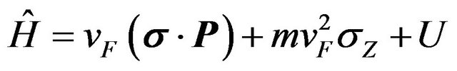
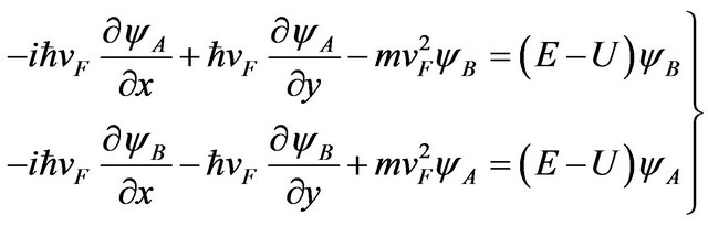
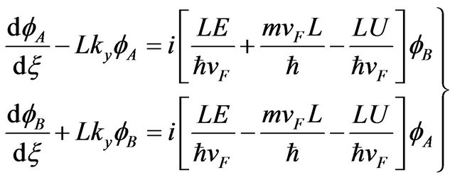
Electrons in graphene can be treated as massless particles. Their behavior is governed by Dirac Hamiltonian [2,5,6]. The Hamiltonian including the energy gaps of the semiconductor film surrounding the graphene strip and a diagonal effective mass-like term  is [2].
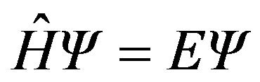
 and the Dirac equation is [2]
 , (1)
, (1)
where
 (2)
(2)
Since effective mass of electrons in graphene strips near the corners of the Brillouin zone is close to massless, the Hamiltonian of the electrons is nearly relativistic. Then the energy of the electrons in the graphene strip mostly arises from the spin-orbit interaction [2,18].
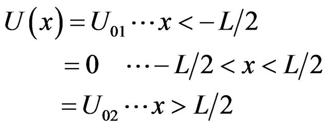
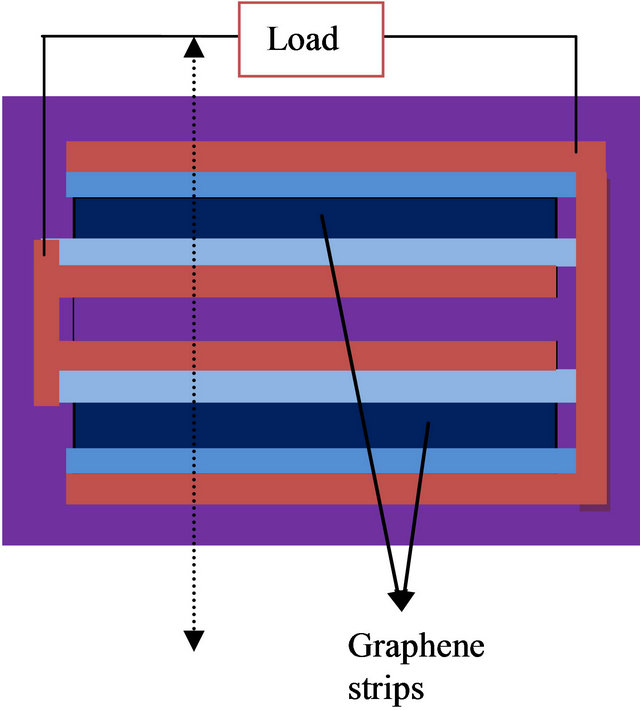
The potentials are the energy gaps of the semiconductors as a barrier around the edges of the graphene strips. The structure of the graphene quantum well is shown in Figure 1.
The scheme of the potential quantum well is shown in Figure 2.
The potential function for the well is
Similarly to Pereira et al.’s work [2], we derived following equations.
 (a)
(a)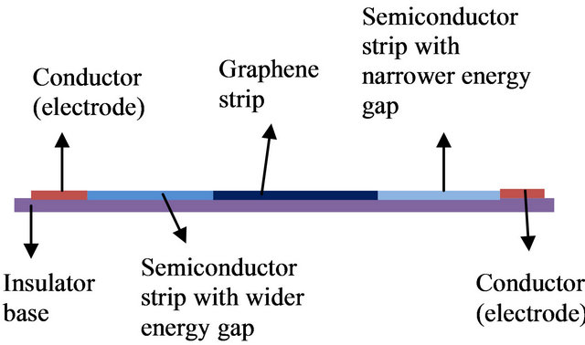 (b)
(b)
Figure 1. (a) Top view of structure of graphene quantum well; (b) Cross section view of structure of graphene quantum well.
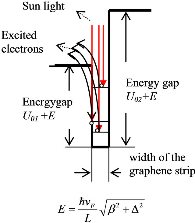
Figure 2. Quantum well.
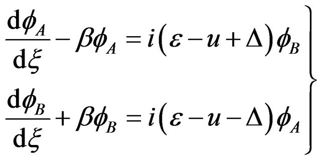
Combining Equations (1) and (2), we found the Equation (3)
 (3) [2]
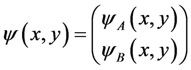
Since y-direction is along the length of the strip which is much greater than the width L, electrons are considered as free particles in y. Then the wave function can be expressed as
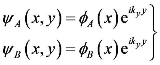 (4) [2]
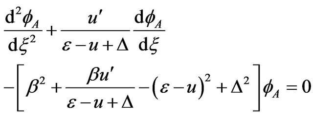
Substituting 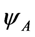 and
and 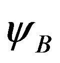 into Equation (3) with Equation (4), Equation (3) become [2]
 (5)
(5)
Letting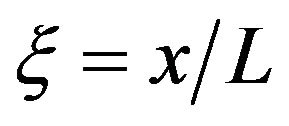 , then Equation (5) become
 (5)’
(5)’
Letting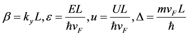 , Equation (5)’ become
 (5)” [2]
From Equation (5)”, we obtained Equation (6)
 (6)
(6)
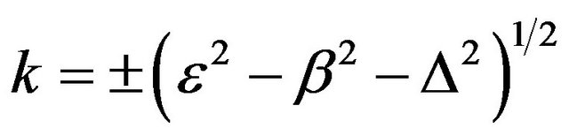
where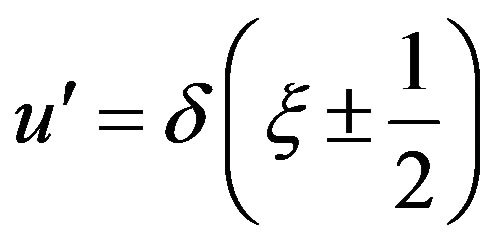 . [2]
. [2]
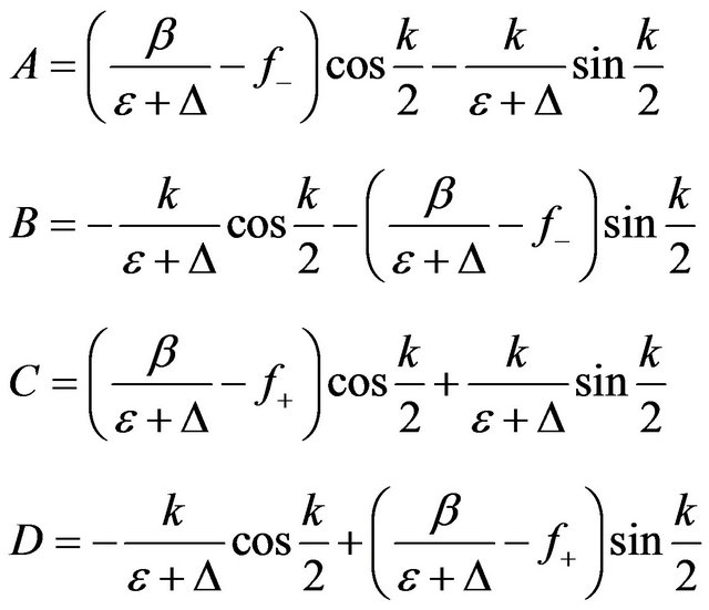
Equations (5)” and (6) with an asymmetric potential shown before have solutions [2]
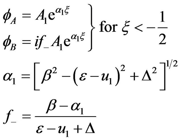
And [2]
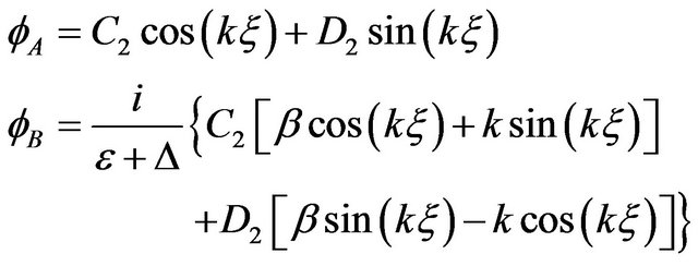
for 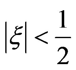
where C2, D2 are constants and
And [2]
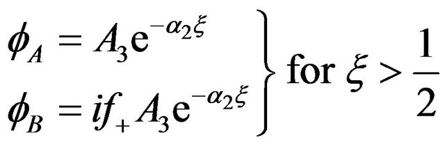
where
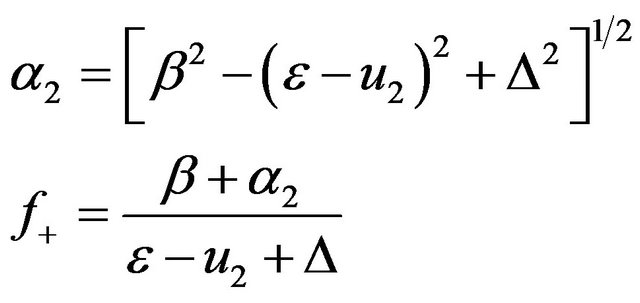
with  and
and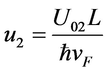 .
.
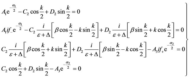
3. Boundary Conditions and the Electron States in Graphene Quantum Well
It has been proven that the probability flow densities 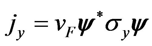 at boundary
  is continuous. The wave functions
  and their derivatives are continuous at the boundary too. Then we form the four equations:
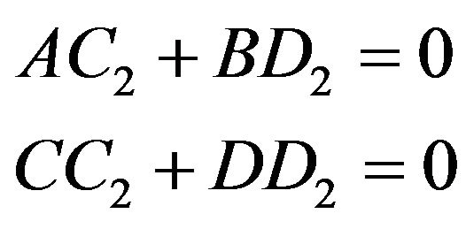
Through algebra processes we reduce these four equations in group (7) into two equations as
where
The characteristics equation or energy quantization equation is a transcendental equation as
 (8)
(8)
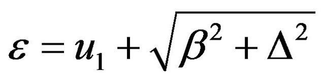
Equation (8) determines the dimensionless energy ε as a function of β, Δ, μ1 and μ2 or energy E as a function of ky, U01, U02, vF and L. This equation can only be solved numerically. Let us discuss the aspect of the solutions in some special cases:
 (7)
(7)
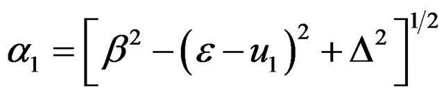
1) For non-relativistic particle if the energy gaps of the surrounding semiconductors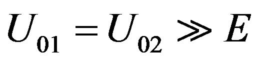 , energy of electrons, as we know that the probability of finding non-relativistic particles outside the well decays experientially as
 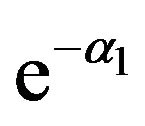 and
and , α1, α2 are positive, hence particles are confined in the well. In contrast, for relativistic particle even in this case α1, α2 can be imaginary number. It may be understood as a manifestation of a relativistic tunneling effect first discussed by Klein [2,19,20]. The electronic states of the epitaxial graphenequantum-well film system was discussed by Alisultanov and Meilanov [21].
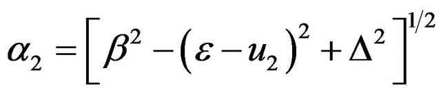
2) For relativistic electron α1, α2 determine the configuration of the electrons, not U01 or U02. α1 and α2 can be real or complex. The confined electron states can only exist when the values of α1, α2 are real. In general, if  the wave functions of massless electrons outside the well decay rapidly like nonrelativistic particle. The massless electrons are also possibly confined in the well. Let us discuss these cases in detail.
Since
if  and real, it leads to 1)
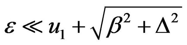
or 2)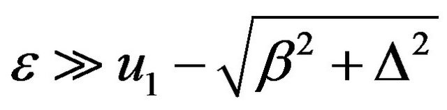 .
.
Similarly since
if 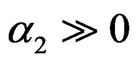 and real, it also leads to 1)’
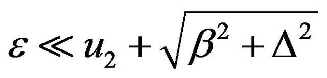
or 2)’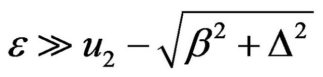 .
.
And because
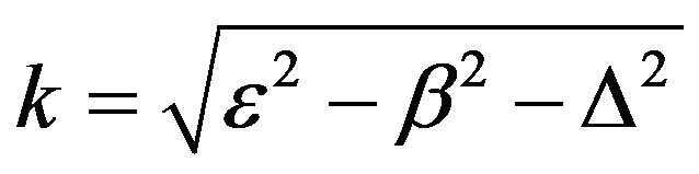
must be real, therefore3) .
.
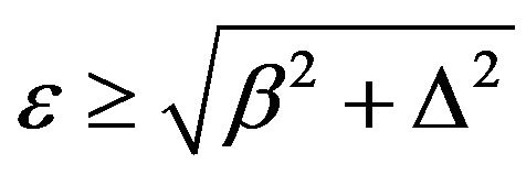
If the electrons are confined in the well, the solution of Equation (8), i.e. ε as a function of β, Δ, μ1 and μ2 or energy E as a function of ky, U01, U02, vF is also restrained by these four conditions mentioned above. The values of ε and β satisfying the above mentioned conditions fall in the area marked by the dashed lines in Figure 3.
4. Numerical Calculation of Energy States and Wave Function in the Well
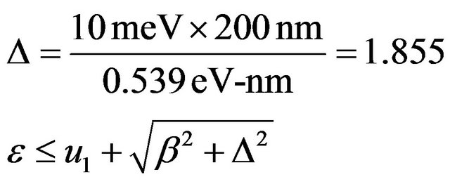
Equation (8) can be solved numerically. For L = 200 nm, U01 = 1.0 eV, energy gap for GaAs and U02 = 1.5 eV, energy gap for GaAsAl. 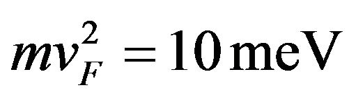 for graphene, the dimensionless parameters are
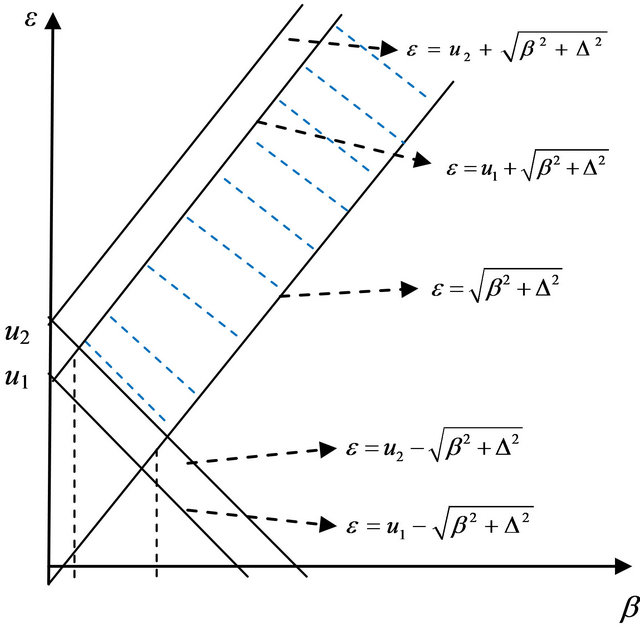
Figure 3. Diagram for the restrained relation of β and ε.
and
and
and
 .
.
According to these conditions mentioned above, in the region (dot lines marked) in β, ε frame there may exist confined states.
We can choose different values of β and ε to calculate the values of α1, α2 and k, and do algorism on Equation (8) until finding the value or values of ε that satisfy this equation. There are possible discrete energy states, if for one value of β there are multiple values of ε that satisfy Equation (8).
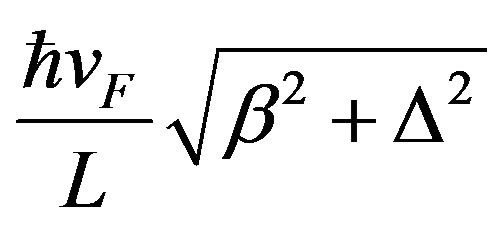
The numerical calculation results are shown in Figure 4. From Figure 4 we show the dimensionless energy ε as a function of β. One can see that there are multiple of energy levels for each value of β. Then electrons occupying these states can absorb photons with different frequencies and exited to the states where the energy level is higher than . Converting to real energy, that is
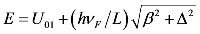
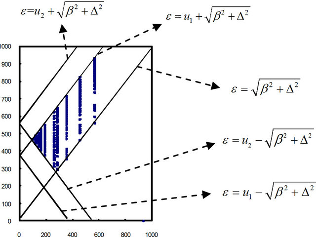
Figure 4. The numerical calculation result showing ε vs β.
The efficiency of the photovoltaic device made of such quantum well is expected to be higher.
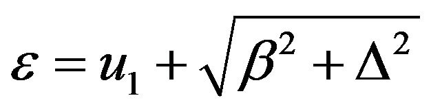
According to the spectrum of sun light, the photo energies of sun light range from 0.5 eV to 2.9 eV. The energy levels of electrons inside the well range from
 to
to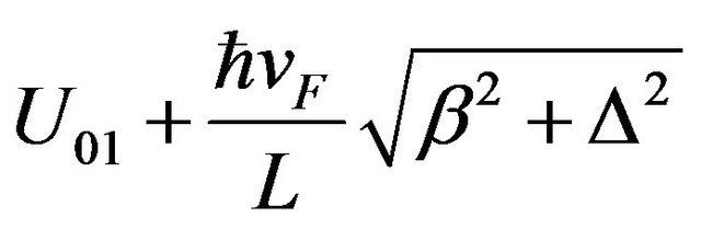 . U01 should be relatively large, so that there would be enough number of electrons confined in the well. But it can’t be too much larger than 3.0 eV, because if U01 is too large, there may not be enough number of electrons exited to the outside of the well on the semiconductor strip with smaller energy gap. In contract, U02 should be large than U01 + 2.90 eV, so that no much electrons can escape to another side of the well (the semiconductor strip with higher energy gap). Dr. Alex Ignatiev is trying to produce GaN with energy gap of 3.5 eV [22]. It may serve well for this purpose.
5. Conclusion
Our theoretical study of quantum well based on graphene and semiconductors with two different energy gaps has shown that the behavior of low energy carrier of 2 D gas massless charged fermions including a diagonal effective mass-like term  is governed by the 2 D Dirac equation. The 2 D Dirac equation has been solved numerically. The results indicate that the graphene quantum well possesses very dense quantum energy states which imply that quantum well of this type can absorb sun light with more different frequencies. If we use graphene quantum well to fabricate the photo voltaic cell, the efficiency of converting solar energy to electricity will be enhanced. The quantum well with uneven gaps of the semiconductors at the edges of the graphene strip provides a perfect electric parity for the photo voltaic cell.
6. Acknowledgements
The work is partially supported by Air Force Office of Scientific Research (Award No. FA9550-09-1-0367) and the National Science Foundation (Award No. CBET- 0754821).
REFERENCES
- L.-P. An, T.-B. Wang and N.-H. Liu, “Inter-Well Coupling and Resonant Tunneling Modes of Multiple Graphene Quantum Wells,” Communications in Theoretical Physics, Vol. 56, No. 2, 2011, pp. 367-372. doi:10.1088/0253-6102/56/2/29
- J. M. Pereira Jr, V. Mlinar and F. M. Peeters, “Confined States and Direction-Dependent Transmission in Graphene Quantum Wells,” Physical Review B, Vol. 74, No. 4, 2006, pp. 1-5.
- P. R. Wallace, “The Band Theory of Graphite,” Physical Review, Vol. 71, No. 9, 1947, pp. 622-634. doi:10.1103/PhysRev.71.622
- M. Wilson, Physics Today, 2006, p. 21.
- G. W. Semenoff, “Condensed-Matter Simulation of a Three-Dimensional Anomaly,” Physical Review Letters, Vol. 53, No. 26, 1984, pp. 2449-2452. doi:10.1103/PhysRevLett.53.2449c
- I. A. Luk’yanchuk and Y. Kopelevich, “Phase Analysis of Quantum Oscillations in Graphite,” Physical Review Letters, Vol. 93, No. 16, 2004, pp. 166402-166406. doi:10.1103/PhysRevLett.93.166402
- L. A. Ponomarenko, F. Schedin, M. I. Katsnelson, et al., Science, Vol. 320, 2008, p. 356.
- T. Ando, “Theory of Electronic States and Transport in Carbon Nanotubes,” Journal of the Physical Society of Japan, Vol. 74, 2005, pp. 777-817. doi:10.1143/JPSJ.74.777
- P. V. Ratnikov and A. P. Silin, “Quantum Well Based on Graphene and Narrow-Gap Semiconductors,” Bulletin of the Lebedev Physics Institute, Vol. 36, No. 2, 2009, pp. 34-43. doi:10.3103/S106833560902002X
- K. S. Novoselov, A. K. Geim, S. V. Morozov, et al., Nature, Vol. 438, 2005, p. 197.
- Y. Zhang, Y.-W. Tan, H. L. Stormer and P. Kim, Nature, Vol. 438, 2005, p. 201. doi:10.1038/nature04235
- L. Brey and H. A. Fertig, “Electronic States of Graphene Nanoribbons Studied with the Dirac Equation,” Physical Review B, Vol. 73, No. 23, 2006, pp. 235411-235416. doi:10.1103/PhysRevB.73.235411
- L. Brey and H. A. Fertig, “Elementary Electronic Excitations in Graphene Nanoribbons,” Physical Review B, Vol. 75, No. 12, 2007, pp. 125434-125440. doi:10.1103/PhysRevB.75.125434
- Y.-W. Son, M. L. Cohen and S. G. Louie, “Energy Gaps in Graphene Nanoribbons,” Physical Review Letters, Vol. 97, No. 21, 2006, pp. 216803-216807. doi:10.1103/PhysRevLett.97.216803
- E. Mccann and V. I. Fal’ko, “Symmetry of Boundary Conditions of the Dirac Equation for Electrons in Carbon Nanotubes,” Journal of Physics: Condensed Matter, Vol. 16, No. 13, 2004, p. 2371. doi:10.1088/0953-8984/16/13/016
- X. Wang, Y. Ouyang, X. Li, et al., “Room-Temperature All-Semiconducting Sub-10-nm Graphene Nanoribbon Field-Effect Transistors,” Physical Review Letters, Vol. 100, No. 20, 2008, pp. 206803-206807. doi:10.1103/PhysRevLett.100.206803
- R. Saito, G. Dresselhaus and M. S. Dresselhaus, “Physical Properties of Carbon Nanotubes,” Imperial College Press, London, 1998.
- C. L. Kane and E. J. Mele, “Quantum Spin Hall Effect in Graphene,” Physical Review Letters, Vol. 95, No. 22, 2005, pp. 226801-226805. doi:10.1103/PhysRevLett.95.226801
- O. Klein, “Die Reflexion von Elektronen an Einem Potentialsprung Nach der Relativistischen Dynamik von Dirac,” Zeitschrift für Physik, Vol. 53, No. 3-4, 1929, pp. 157-165. doi:10.1007/BF01339716
- N. Dombey and A. Calogeracos, “Seventy Years of the Klein Paradox,” Physics Reports, Vol. 315, No. 1-3, 1999, pp. 41-58. doi:10.1016/S0370-1573(99, 00023-X
- Z. Z. Alisultanov and R. P. Meilanov, “On the Theory of Electronic States of the ‘Epitaxial Graphene-QuantumWell Film’ System,” Physics of Solid State, 2012, Vol. 54, No. 7, pp. 1486-1493. doi:10.1134/S1063783412070037
- A. Ignatieve, “Professor of Physics, Chemistry, and Computer Science,” Private Communication, 2012.