Journal of Electromagnetic Analysis and Applications
Vol. 1 No. 1 (2009) , Article ID: 198 , 7 pages DOI:10.4236/jemaa.2009.11011
Analysis and Design of a Kind of Improved Parallel Resonant Converters
1School of Information and Communication of Tianjin Polytechnic University, Tianjin, China, 2School of Electrical Engineering and Automation of Tianjin University, Tianjin, China.
Email: Yuanfei791019@163.com
Received January 6th, 2009; revised February 3rd, 2009; accepted February 18th, 2009.
Keywords: Power Converters, Parallel Resonant, Voltage-Doubler Rectifier, High-Voltage Power Supply
ABSTRACT
Traditional transformer in high-voltage power supplies has many disadvantages such as high turn’s ratio, large volume and great design difficulties. Parallel resonant converters (PRCs) are widely used in high-voltage power supplies. A kind of high-voltage circuit topology can be formed by combining PRCs and voltage-doubler rectifier, which is called parallel resonant dual voltage converters (PRDVCs). In PRDVCs both voltage-doubler rectifier and transformer can boost voltage, which reduced turn’s ratio and volume of the transformer, making it easier to produce. Thus it not only realizes the high-voltage output, but also realizes the miniaturization of high-voltage power supply. Three modes of the converters were researched and simulated. Converting conditions of three modes were given. At last, PRDVCs was used to design a 5000V/50mA high-voltage power supply. The waveforms and results of the experiment were given, which validated the feasibility of the converters and its conversion efficiency might be improved to 93%.
1. Introduction
High-voltage power supplies have been widely used in inspection equipments such as medicine, non-destructive testing, station, customs inspection and also been used for military purposes such as radar transmitters, electronic chart monitor in aviation light. Traditional high-voltage power supplies have affected development of corollary equipments because of large volume and heavy weight. At present, SMPS schemes have been widely adopted in high-voltage power supplies. It made the volume and weight be greatly reduced and power capacity and conversion efficiency be increased, especially embodied in small power high-voltage SMPS. Yet for all that, turn’s ratio and volume of transformer were still very large and its difficulties in design and manufacture were still existent. For this reason, using the good adaptability of PRCs to high-voltage power supplies, A kind of high-voltage circuit topology can be formed by combining PRCs and oltage-doubler rectifier, which is parallel resonant dual voltage converters (PRDVCs) [1]. As a kind of improved parallel resonant high-voltage SMPS topology, PRDVCs can increase switch frequency and conversion efficiency by using soft switching technology. Both voltage-doubler rectifier and transformer can boost voltage, which made turn’s ratio and volume of the transformer be greatly reduced, making it easier to produce. Thus it realized the miniaturization and lightweight of high-voltage power supply. In Section 2, the basic circuit topology of PRDVCs was introduced. In Section 3, work modals of PRDVCs were analyzed. In Section 4, three Modes were studied. In Section 5, converting conditions of three modes were deduced. In Section 6, three Modes were verified by PSPICE. In Section 7, a 5000V/50mA highvoltage power supply was designed by using PRDVCs.
2. Basic Circuit Topology of PRDVCs
PRDVCs was the improvement of PRCs (as shown in Figure 1). Two kinds of basic topologies of PRDVCs were given in Figure 2. One was the half-bridge parallel resonant dual voltage converter (HBPRDVC) and the other was full-bridge parallel resonant dual voltage converter (FBPRDVC), where  was the resonant inductance,
  was the resonant capacitance,
  was load. Here the role of transformer was not only voltage transfer but also electrical isolation. Compared with PRCs, two capacitances were adopted to replace two rectifying diodes and the heavy inductance was omitted in PRDVCs circuit topology.

Figure 1. PRCs
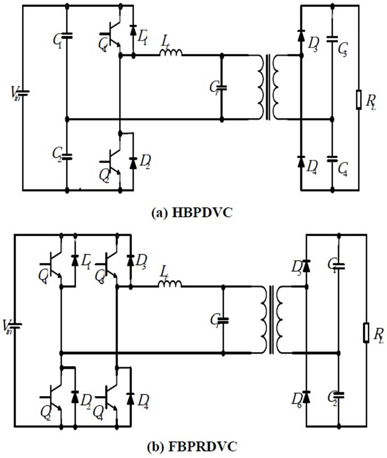
Figure 2. Basic circuit topologies of PRDVCs
3. Analysis for Work Modals of PRDVCs
Full bridge topology and half bridge topology work on the same principle [2]. In this paper, we took HBPDVC for example to research PRDVCs. For convenience transformer’s ratio was declared equivalent to 1. Transformer was equivalent to excitation inductance and its leakage inductance was neglected. Then the equivalent circuit could be seen in Figure 3. Here the direction of voltage and current was reference direction. Before analyzing PRDVCs, some reasonable conditions should be assumed as follows. 1) Q1, Q2, D1, D2, D3, D4 were ideal switching tubes. 2) During a switching cycle both input voltage and output voltage were constants. C1, C2, C3, C4 were large enough. Electric potential of node A was  and electric potential of node O was
 . 3) Both inductance and capacitance were lossless energy storage elements. 4) line impedance was not considerable.
Under above conditions, PRDVCs had four resonant switching modals (as shown in Figure 4) and four linear switching modals (as shown in Figure 5). Where  was the resonant inductance,
  was the resonant capacitance,
  was the excitation inductance. The directions of arrows were real directions. In Figure 4 and Figure 5, it could be seen that switching tubes and directions of
  and
and  were different from one modal to anther.
Equivalent circuit of resonant switching modals was shown in Figure 6. The corresponding relations between  and conducting components and resonant inductance current were given in Table 1.
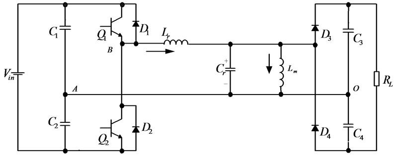
Figure 3. Equivalent circuit of PRDVCs
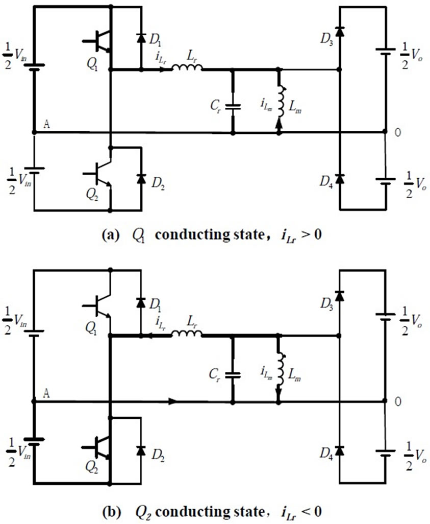
Figure 4. Four resonant switching modals
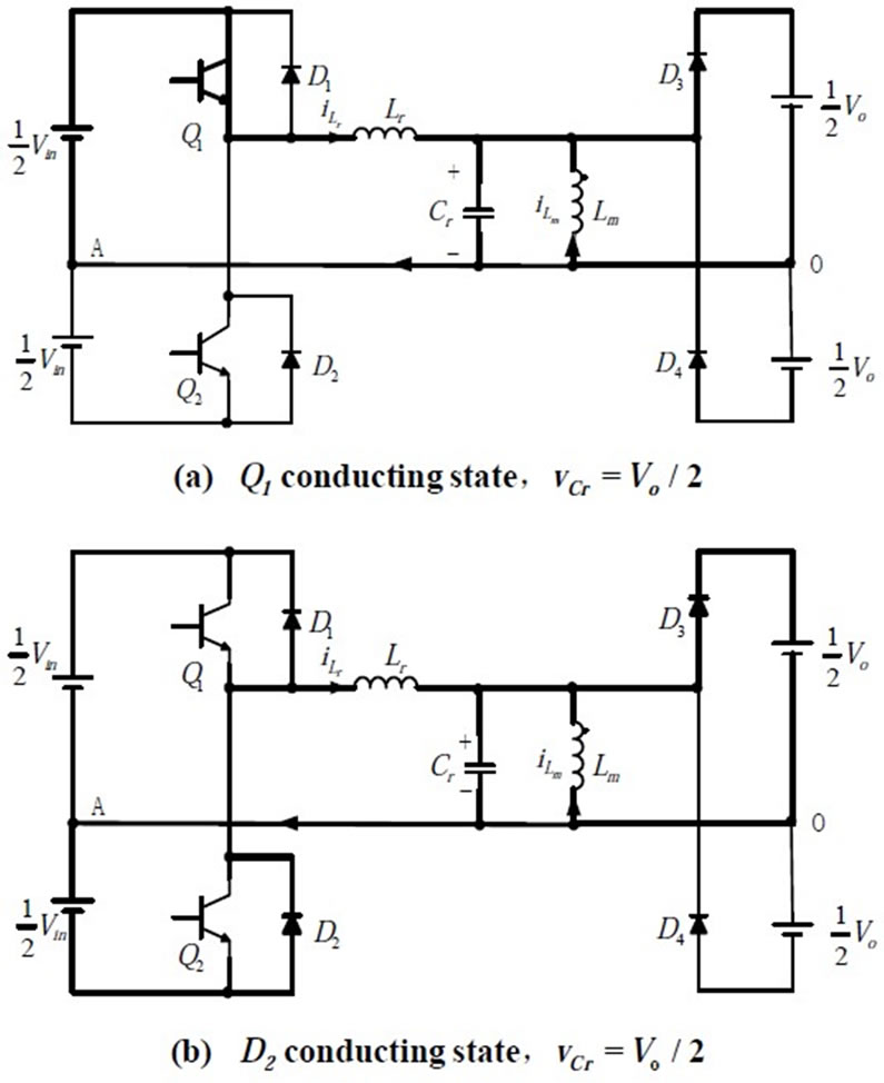
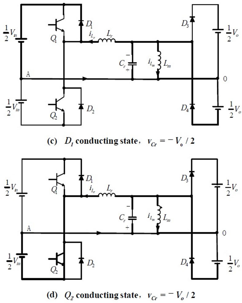
Figure 5. Four linear switching modals
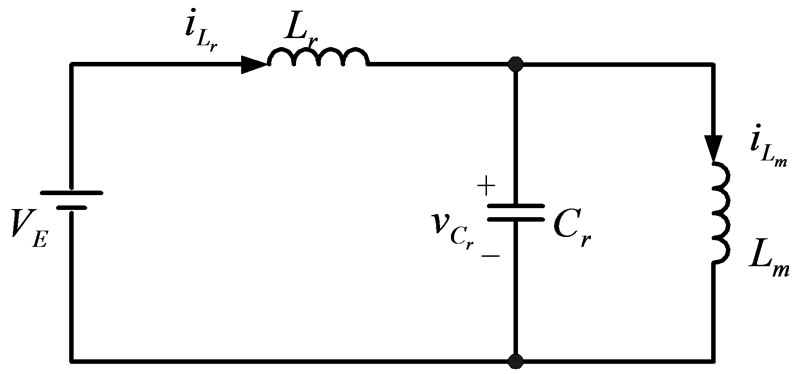
Figure 6. Equivalent circuit of resonant Switching modals
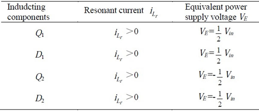
Table 1. The corresponding relations between  and conducting components and resonant inductance current
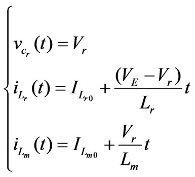
Analyzing the equivalent circuit in Figure 6, differential equations were shown as (1).
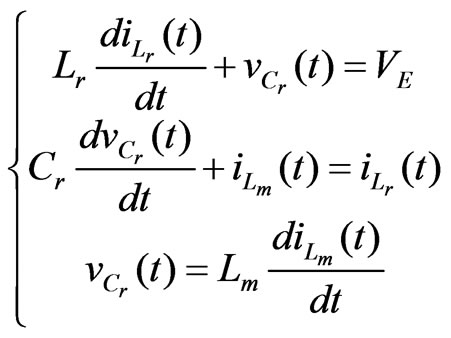 (1)
(1)
The initial conditions were assumed as follows.
when  »
» , general mathematic expressions of
 ,
,  ,
,  could be shown as (2).
 (2)
(2)
where .
.
Equivalent circuit of linear switching modals was shown in Figure 8. The corresponding relations between  and conducting components and capacitance voltage were given in Table 2.
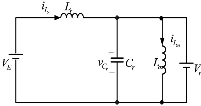
Figure 7. Equivalent circuit of linear switching modals
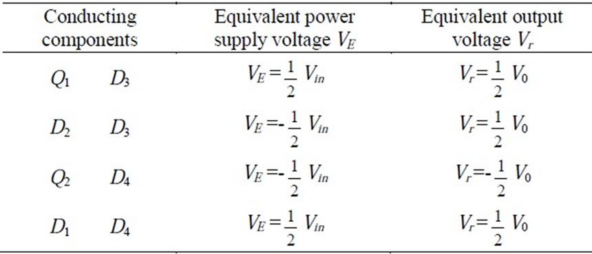
Table 2. The corresponding relations between VE and conducting components and capacitance voltage
The initial conditions were assumed as follows.
 ,
,
Analyzing equivalent circuit general mathematic expressions of ,
,  ,
,  could be shown as (3).
 (3)
(3)
4. Three Modes of PRDVCs
PRDVCs appeared three operational modes when loads and operational ranges changed.
4.1 Operational Mode 1
Selecting logical parameters Mode 1 appeared. Steady operating waveforms of Mode 1 were shown in Figure 8. One switching cycle could be divided into six switching modals.
4.1.1 Switching Modal 1 [t0-t1]
Before t0 moment Q1 and D3 were conducting, Q2, D1, D2, D4 were off. At t0 moment Q1 would be turned off. D2 would be conducted because of continuous , and then Q2 would be put into operation by ZVS. During this period,
  was constant and
  would be decreased
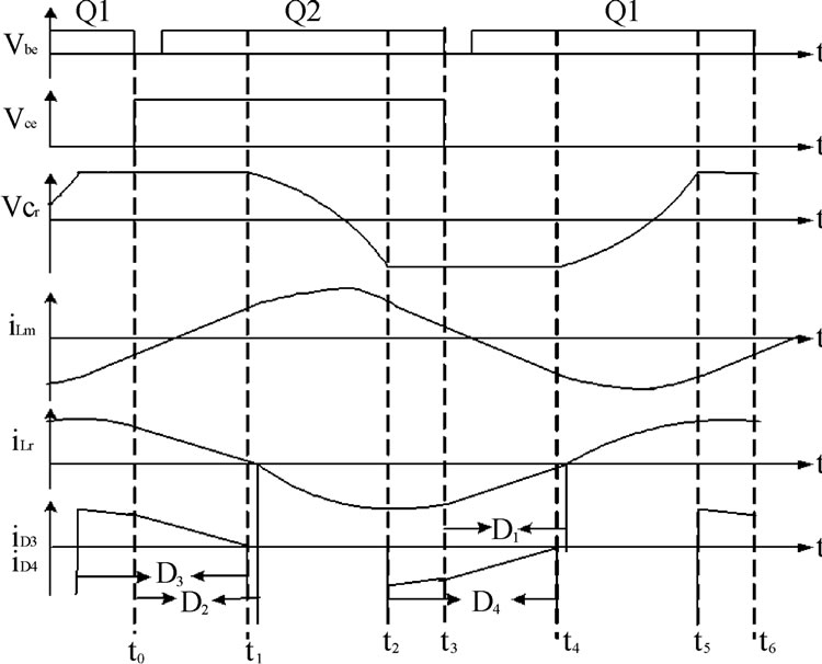
Figure 8. Steady operating waveforms of Mode 1
linearly and  would be increased linearly. Here stored energy. In inductance would be transmitted to load, as shown in Figure 5(b). Substituting initial conditions to (3), the corresponding mathematic models of
 ,
,  ,
,  could be deduced.
4.1.2 Switching Modal 2 [t1-t2]
At t1 moment,  and D3 would shut off naturally. Then D2 would shut off naturally too.
  would be increased reversely and
  would be increased positively. Here circuit state would be transferred from linear modal to resonant modal, as shown in Figure 4 (b). Substituting initial conditions to (2), the corresponding mathematic models of
 ,
,  ,
,  could be deduced.
4.1.3 Switching Modal 3 [t2-t3]
At t2 moment,  and
and  was conducted. Here circuit state would be transferred from resonant Modal to linear modal. During this period,
  was constant and
  would be linearly decreased reversely and
  would be linearly decreased positively. Here stored energy in inductance would be transmitted to load, as shown in Figure 5(d). Substituting initial conditions to (3), the corresponding mathematic models of
 ,
,  ,
,  could be deduced.
4.1.4 The second half of cycle [t3-t6]
After t3 moment circuit state would enter the second half of cycle. These were similar to the first half.
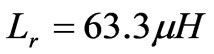
4.2 Operational Mode 2
When switching frequency was higher than resonant frequency, PRDVCs would be shifted from Mode 1 to Mode 2 with the decreasing load. Steady operating waveforms of Mode 2 were shown in Figure 9. One switching cycle could be divided into six switching modals.
4.2.1 Switching Modal 1 [t0-t1]
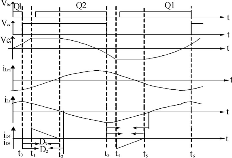
Figure 9. Steady operating waveforms of Mode 2
Before t0 moment, Q1 was conducting and Q2, D1, D2, D3, D4 were off. At t0 moment, Q1 would be turned off and D2 would be conducted because of continuous . During this period circuit was in resonant state, as shown in Figure 4(d). Substituting initial conditions to (2), the corresponding mathematic models of
 ,
,  ,
,  could be deduced.
4.2.2 Switching Modal 2 [t1-t2]
At t1 moment,  would rise to
  and D3 would be conducted. Then Q2 would be put into operation by ZVS. During this period,
  was constant and
  would be linearly decreased positively and
  would be linearly decreased reversely. Here stored energy in inductance would be transmitted to load, as shown in Fig.5 (b). Substituting initial conditions to (3), the corresponding mathematic models of
 ,
,  ,
,  could be deduced.
4.2.3 Switching Modal 3 [t2-t3]
At t2 moment,  and D3 would shut off naturally. Then D2 would shut off naturally too.
  would be increased reversely and
  would be increased positively. Here circuit state would be transferred from linear modal to resonant modal, as shown in Figure 4 (b). Substituting initial conditions to (2), the corresponding mathematic models of
 ,
,  ,
,  could be deduced.
4.2.4 The second half of cycle [t3-t6]
After t3 moment, circuit state would enter the second half of cycle. These were similar to the first half.
4.3 Operational Mode 3
When switching frequency was lower than resonant frequency,PRDVCs would be shifted from Mode 1 to Mode 3 with decreasing load. Steady operating waveforms of Mode 3 were shown in Figure 10. One switching cycle could be divided into six switching modals.
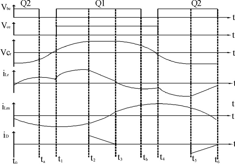
Figure 10. Steady operating waveforms of Mode 3
4.3.1 Switching Modal 1 [t0-t1]
Before t0 moment, Q2 and D4 were conducting, Q1, D1, D2, D3 were off. During this period, circuit was in linear state. At t0 moment,  and D4 would shut off naturally. Then D2 would be conducted and circuit state would be transferred from linear modal to resonant modal. At ta moment, Q2 would be turned off by ZCS, as shown in Figure 4(d). Substituting initial conditions to (2), the corresponding mathematic models of
 ,
,  ,
,  could be deduced.
4.3.2 Switching Modal 2 [t1-t2]
At t1 moment, Q1 would be put into operation and D2 would be shut off. This was a hard switching and would lead to switching loss. Here circuit was still in resonant state, as shown in Figure 4 (a). Substituting initial conditions to (2), the corresponding mathematic models of ,
,  ,
,  could be deduced.
4.3.3 Switching Modal 3 [t2-t3]
At t2 moment,  would rise to
  and D3 would be conducted. Here circuit state would be transferred resonant modal to linear modal and stored energy in inductance would be transmitted to load, as shown in Figure 5 (a). Substituting initial conditions to (3), the corresponding mathematic models of
 ,
,  ,
,  could be deduced.
4.3.4 The second half of cycle [t3-t6]
After t3 moment, circuit state would enter the second half of cycle. These were similar to the first half.
5. Converting Conditions of Three Modes
Defined ,
,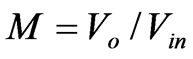 . Steady output voltage could be acquired by PFM when PRDVCs was applied. With load being reduced, the steady output voltage could be realized by increasing or decreasing the switching frequency.
When switching frequency increased, PRDVCs state would be converted from Mode 1 to Mode 2. The critical frequency was 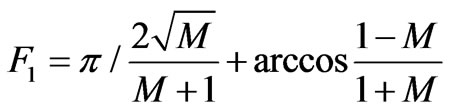 (apparently M>0, F1≥1). When F<F1, leading to Mode 1. When
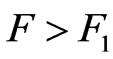 , leading to Mode 2. When switching frequency decreased, PRDVCs would shift from Mode 1 to Mode 3. The critical frequency was
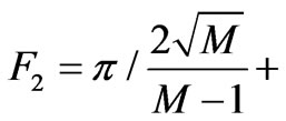
 (apparently M≥1, F2≤1). When F>F2, leading to Mode 1, When F>F2, leading to Mode 3.
6. Simulation Experiments for Three Modes
For verifying the analyzed results, some simulation experiments were carried on by Pspice. The simulation parameters were as follows.
Input direct voltage: Vin ;
;
Output direct voltage: Vo ;
;
Q1(D1)-Q4(D4): IRPF640;
Resonant parameters: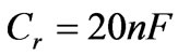
 ;
;
Mode 1: Switching frequency ;
;
Output power; 
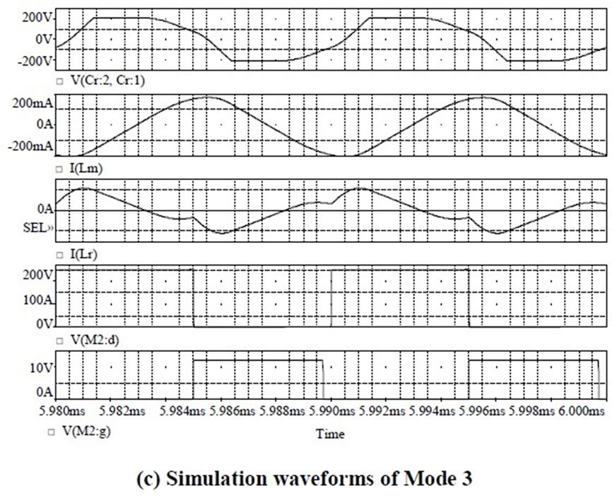
Figure 11. Simulation waveforms of three Modes
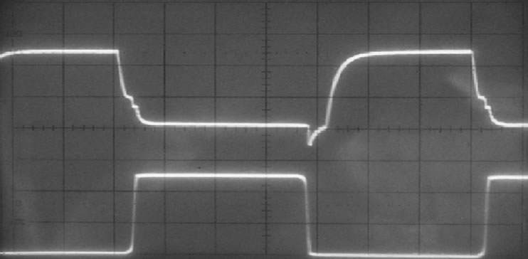
Figure 12. Waveforms of experimental circuit
Mode 2: Switching frequency 
Output power ;
;
Mode 3: Switching frequency ;
;
Output power .
.
Simulation waveforms of three modes were shown in Figure 11. It was verified that the analyzed results were correct.
7. Design of 5000V Power Supply
In this section, a 5000V/50mA high-voltage power supply was designed by applying HBPRDVC. The design parameters were given as follows.
Input direct voltage: 250VDC;
Switching frequency: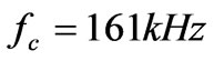 ;
;
Resonant inductance: ;
;
Resonant capacitance: ;
;
Output direct voltage: 5000VDC;
Full load: 250W;
Power tubes: IRPF460;
Ratio of transformer: n=5.55;
Under above parameters, PRDVCs operated in Mode 1 when full load. The 5000V/50mA power supply was realized by experiments. The power supply was high performance. It was verified that PRDVCs is feasible for high-voltage power supply. Under full load condition, the relationship between the voltage across power tube and its trigger pulse was given, as shown in Figure 12. Apparently, power tubes were conducted by ZVS. The conversion efficiency was up to 93%.
8. Conclusions
A 5000V/50mA high-voltage power supply was built by HBPRDVC. It was verified that the plan is feasible by experiment results. Compared with traditional plans of high-voltage power supplies,  has following merits: 1) Soft switching was realized by resonant technology, thereby switching frequency and conversion efficiency were boosted; 2) Distributed capacitance and leakage inductance in high-frequency transformer were available. The influence of distributed parameters was reduced and EMC of the power system was improved. Thus the reliability of the converters was ensured; 3) Both voltage-doubler rectifier and transformer could boost voltage, which reduced turn’s ratio and volume of the transformer, making it easier to produce. Therefore, the miniaturization of high-voltage power supply was realized. In summary,
  was applied to pint-size high-voltage and low-current SMPS, which is worthy of broad application prospect.
REFERENCES
- R. W. Erickson, “The parallel resonant converter,” lecture of University of Colorado, chapter 5, 2003.
- X. B. Ruan and Y. G. Yan, “Soft switching technology of
- DC switching power supply [M],” Beijing: Science Press,
- 2003.
- R. Oruganti and F. C. Lee, “State-plane analysis of a parallel resonant converter,” [C]. IEEE Power Electronics Specialist Conference Record, PESC-1985, pp. 56-73.
- A. K. S. Bhat and M. M. swamy, “Analysis and design of a high-frequency parallel resonant converter operating above resonance,” [J]. IEEE Transactions on Aerospace and electronics Systems, Vol. 25, No. 4, pp. 449-458, July 1989.
- Z. G. Lu, “Computer simulation of power supply,” [M]. Beijing: Science Press, 2001.