Circuits and Systems
Vol.4 No.2(2013), Article ID:29884,8 pages DOI:10.4236/cs.2013.42028
A New Technique for Leakage Reduction in 65 nm Footerless Domino Circuits
Department of Electronics & Communication, Maulana Azad National Institute of Technology, Bhopal, India
Email: taruniet@rediffmail.com
Copyright © 2013 Tarun Kumar Gupta, Kavita Khare. This is an open access article distributed under the Creative Commons Attribution License, which permits unrestricted use, distribution, and reproduction in any medium, provided the original work is properly cited.
Received June 27, 2012; revised February 1, 2013; accepted February 8, 2013
Keywords: Footerless Domino Logic; Subthreshold Leakage; Gate Oxide Tunneling; Leakage Current
ABSTRACT
A new circuit technique for 65 nm technology is proposed in this paper for reducing the subthreshold and gate oxide leakage currents in idle and non idle mode of operation for footerless domino circuits. In this technique a p-type and an n-type leakage controlled transistors (LCTs) are introduced between the pull-up and pull-down network and the gate of one is controlled by the source of the other. For any combination of input, one of the LCT will operate near its cut off region and will increase the resistance between supply voltage and ground resulting in reduced leakage current. Furthermore, the leakage current is suppressed at the output inverter circuit by inserting a transistor below the n-type transistor of the inverter offering more resistive path between supply voltage and ground. The proposed technique is applied on benchmark circuits reduction of active power consumption is observed from 10.9% to 44.76% at different temperature variations. For same benchmark circuits, operating at two clock modes and giving low and high inputs at 25˚C and 110˚C temperatures the maximum leakage power saving of 98.9% is achieved when compared to standard footerless domino logic circuits.
1. Introduction
For high-speed chip performance domino circuits are employed and can be classified into footerless and footed domino [1-3]. For better timing characteristics footed domino is used because here the footer transistor isolates the pull-down network (PDN) from ground preventing the change in the state of the dynamic node by PDN during precharge phase. In addition if the footer transistor is omitted, the footerless domino reduces both the circuit evaluation delay and the power consumption. Having different characteristics, the footerless and footed domino based domino circuits both are extensively in high performance processors. For multistage domino circuits, the first stage is typically kept footed and others are footerless [3].
High leakage current in nanometer regime becomes a significant contributor to power dissipation of CMOS circuits as threshold voltage, channel length, and gate oxide thickness are reduced. Consequently, the identification and modeling of different leakage components is very important for estimation and reduction of leakage power, especially for low-power applications. Leakage power depends on gate length and oxide thickness and it varies exponentially with threshold voltage and other parameters. Reduction of supply voltages and threshold voltages for MOS transistors helps to reduce dynamic power dissipation but simultaneously leakage power increases. Leakage mechanism includes the following:
Subthreshold leakage current (Isub) in MOS transistors, which occurs when the gate voltage is below the threshold voltage and mainly, consists of diffusion current [4]. Off-state leakage in present-day devices is usually dominated by this type of leakage. An effect called drain-induced barrier lowering (DIBL) takes place when a highdrain voltage is applied to a short channel device. The source injects carriers into the channel surface (independent of gate voltage). Narrow width of the transistor can also modulate the threshold voltage and the subthreshold current [4].
 (1.1)
(1.1)
where, µ0 is the zero bias mobility, Cox is the gate oxide capacitance, and (W/L) represents the width to the length ratio of the leaking MOS device. The variable V in equation (1.1) is the thermal voltage constant, and Vgs represents the gate to the source voltage. The parameter n in equation 1.1 is the sub-threshold swing coefficient given by  with Cd being the depletion layer capacitance of the source/drain junction. One important point about Equation (1.1) is that the sub threshold leakage current is exponentially proportional to
 . Shorter channel length results in lower threshold voltages and increases subthreshold leakage. As temperature increases, subthreshold leakage is also increased. On the other hand, when the well-to-source junction of a MOSFET is reverse biased, there is a body effect that increases the threshold voltage and decreases subthreshold leakage.
Gate oxide tunneling current (Igate) in which tunneling of electrons that can result in leakage when there is a high electric field across a thin gate oxide layer. Electrons may tunnel into the conduction band of the oxide layer; this is called Fowler-Nordheim tunneling. In oxide layers less than 3 - 4 nm thick, there can also be direct tunneling through the silicon oxide layer. Mechanisms for direct tunneling include electron tunneling in the conduction band, electron tunneling in the valence band, and hole tunneling in the valence band [5].
Junction leakage that results from minority carrier diffusion and drift near the edge of depletion regions, and also from generation of electron hole pairs in the depletion regions of reverse-bias junctions. When both n regions and p regions are heavily doped, as is the case for some advanced MOSFETs, there is also junction leakage due to band-to-band tunneling (BTBT) [6].
Hot-carrier injection occurs in short-channel transistors. Because of a strong electric field near the silicon/ silicon oxide interface, electrons or holes can gain enough energy to cross the interface and enter the oxide layer. Injection of electrons is more likely to occur, since they have a lower effective mass and barrier height than holes [7].
Gate-induced drain leakage (GIDL), which is caused by high field effect in the drain junction of MOS transistors. In a negative-channel metal-oxide-semiconductor (NMOS) transistor, when the gate is biased to form accumulation layer in the silicon surface under the gate, the silicon surface has almost the same potential as the ptype substrate, and the surface acts like a p region more heavily doped than the substrate. When the gate is at zero or negative voltage and the drain is at the supply voltage level, there can be a dramatic increase of effects like avalanche multiplication and band-to-band tunneling. Minority carriers underneath the gate are swept to the substrate, completing the GIDL path [8]. Thinner oxide and higher supply voltage increase GIDL.
Punch through leakage, which occurs when there is decreased separation between depletion regions at the drain-substrate and the source-substrate junctions. This occurs in short-channel devices, where this separation is relatively small. Increased reverse bias across the junctions further decreases the separation. When the depletion regions merge, majority carriers in the source enter into the substrate and get collected by the drain, and punch through takes place [9].
In this paper, we study the sources of leakage current in footerless domino and show that Isub and Igate are actually functions of not only inputs applied but also dependent on the clock signal state.
The remainder of the paper is organized as follows. In the next section leakage current analysis in footerless domino is analyzed. In Section 3 proposed low leakage domino circuit is explained. Simulation results are given in Section 4. Finally the conclusions are offered in Section 5.
2. Leakage Current Analysis in Footerless Domino CMOS Circuit
This section is divided into two subsections namely 2.1 and 2.2. In Section 2.1 comparison of sub threshold and gate oxide leakage current produced in PMOS and NMOS transistors is shown. In Section 2.2 working of standard footerless domino is discussed.
2.1. Leakage Current Characteristic Comparison of P-Channel and N-Channel Devices
Maximum gate oxide leakage and sub threshold leakage currents produced by PMOS and NMOS is shown in Figure 1. In Figure 1(a) four components of Igate are shown: Gate to channel tunneling current (Igc), gate-to-source tunneling current (Igs), gate-to-drain tunneling current (Igd) and gate-to-body tunneling current (Igb) [10]. Igs and Igd are the edge tunneling currents from gate to source and drain terminals respectively, through the gate-to-source and gate-to-drain overlap areas. Igc is shared between source and drain terminals [11]. Igb is smaller than the other three components of gate tunneling current and it is typically several orders of magnitude.
As shown in Figure 1(a) maximum gate oxide leakage current flows when the transistor is turned ON and maximum potential difference between gate-to-source and gate-to-drain terminals. As shown in Figure 1(b) maximum sub threshold leakage current flows when the transistor is turned OFF and maximum the potential difference between source and drain terminals.
The probability of electron tunneling is much higher than the probability of hole tunneling through the silicondioxide used as gate oxide in bulk CMOS technology. Simulation results show that Igate of a PMOS device is

Figure 1. States of maximum gate oxide and subthresold leakage current, in NMOS and PMOS transistors. (a) Maximum gate oxide leakage current state; (b) Maximum subthresold leakage current state.
much lower when compared with Igate of NMOS device as shown in Figure 2 with similar physical dimensions (width, length and tox) in a 65 nm technology and at the same potential difference across the gate insulator. The Igate produced by an NMOS transistor is 81.5 times higher at supply voltage 1.2 V and 16 times higher at supply voltage of 0.2 V when compared with PMOS transistor. The difference of Igate between NMOS and PMOS transistor is increased with increase of supply voltage as illustrated in Figure 2.
2.2. Standard Footerless Domino Logic
The standard footerless domino logic is shown in Figure 3. In standard footerless domino logic, feedback keeper transistor parallel with precharge transistor whose gate is biased with the output voltage is employed to maintain the dynamic voltage against coupling noise, charge sharing problem and subthreshold leakage current [12].
The working of standard footerless domino circuit is as follows: When the clock is low or during non-ideal mode the prechrage transistor MP1 is ON and charges the dynamic node, this phase is called precharge phase. During the precharge phase output node goes low and MP2 transistor turns ON maintaining the dynamic node in the high state. The output of the domino logic is independent of the inputs applied at the evaluation network only the leakage current is dependent on the input vectors applied. Now when the clock is high or during ideal mode transistor, MP1 is OFF and transistor MP2 is dependent on the output of the domino circuit, this phase is called evaluation phase. The dynamic node charging will depend on the input vectors applied and according to that output node will be low or high. The subthreshold and gate oxide leakage will also depend on the input vectors.
3. Proposed Domino Logic
The proposed circuit technique effectively enhances the reduction of subthreshold and gate oxide leakage simultaneously. The proposed circuit is illustrated in Figure 4. The concept behind the approach is the reduction of leakage power using the effective stacking of transistor between the path from supply voltage to ground. The ob-

Figure 2. Comparison of gate oxide leakage current produced by a NMOS and PMOS transistors with same physical dimensions.
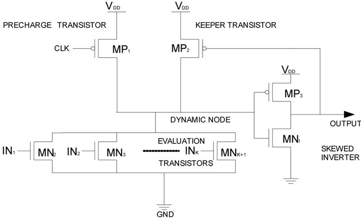
Figure 3. Standard footerless domino logic OR gate.
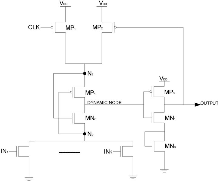
Figure 4. Proposed domino logic OR gate.
servation is based on [13-15] in which a state with only one transistor is OFF between the supply voltage and ground is more leaky then the state with more than one transistor is OFF in a path from supply voltage to ground.
In our approach a transistor MP4 (PMOS) and transistor MN2 (NMOS) LCTs are introduced between the precharge and evaluation network and the gate of these transistors are controlled by the source of each other. The drain node of MP4 and MN2 are connected together to form the input of the inverter. In this configuration, transistor MP4 and MN2 switching will depend on the voltage potential at node N2 and N1 respectively. So for any combination of input in the pull-down network one of the LCT will operate near its cut-off region and increase the resistance between VDD and ground rails leads to the reduction of leakage current.
The working of proposed domino circuit for AND and OR domino gate shown in Figures 5 and 6 respectively is same as standard footerless domino gates. The explanation of leakage reduction of proposed domino circuits in non-ideal mode and ideal mode is as follows: When the clock signal is low or during non-ideal mode the dynamic node is charged high through the transistor MP1 and MP4. The charging of dynamic node is almost independent of the previous clock input state. Suppose if the inputs are low before the clock sets low then node N2 will be at low potential and transistor MP4 offers the less resistance path for charging of dynamic node or if the inputs are high before the clock sets low then the voltage at node N2 is not sufficient to turn MP4 completely to OFF state (MP4 is operating near its cut off region). The resistance of MP4 will be lesser than in OFF resistance allowing the dynamic node to get charge high. The charging of the dynamic node is called precharging phase. In this case output of the domino circuit is independent of the inputs applied at the evaluation network only the leakage current is dependent on the input vectors applied as shown in Figures 5 and 6.
Now when the clock turns high or during ideal mode this is called evaluation phase, depending on the inputs the dynamic node gets charged or discharged. If all the inputs are low the dynamic node will not be discharged by the evaluation network and the output of the inverter will be low and it turns ON the transistor MP2, the voltage at node N1 will turn ON the transistor MN1 but the voltage induced at node N2 will not cut off the transistor MP4 it will operate near cut-off region offering high resistance path between VDD and ground reducing sub threshold and gate leakage current. If all the inputs are high the dynamic node will be discharged through the evaluation network and the output of the inverter will be high. Transistor MP2 will turn OFF, the voltage at node N1 will operate the transistor MN2 near its cut off region again offering high resistance path. The potential at node N2 will turn ON the transistor MP4. So by introducing the LCTs the resistance between VDD and ground is increased
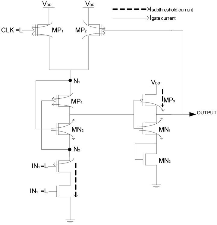
Figure 5. A two-input proposed domino AND gate with low inputs during non-ideal mode. The most significant components of subthreshold and gate oxide leakage currents are illustrated with arrows.
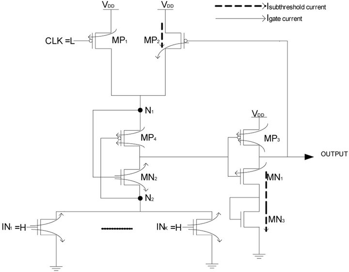
Figure 6. A k-input proposed domino OR gate with high inputs during non-ideal mode. The most significant components of subthreshold and gate oxide leakage currents are illustrated with arrows.
and simultaneously propagation delay of the domino circuit is also increased. The propagation delay will be controlled by sizing of the LCTs. Transistor MN3 is added in the diode-footed configuration below transistor MN1 producing the stacking effect in the inverter and reducing the sub threshold and gate oxide leakage current. In this case, the leakage will also depend on the input vectors as shown in Figures 7 and 8.
The total leakage in domino OR gate increases with the increase of number of inputs (wide-OR) compared
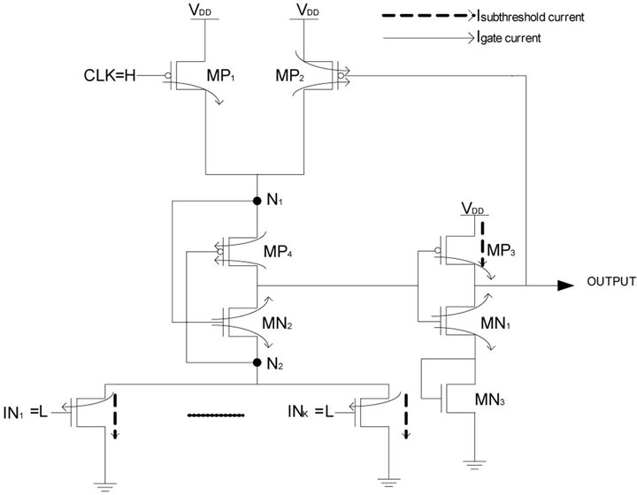
Figure 7. A k-input proposed domino OR gate with low inputs during ideal mode. The most significant components of subthreshold and gate oxide leakage currents are illustrated with arrows.

Figure 8. A k-input proposed domino OR gate with high inputs during ideal mode. The most significant components of subthreshold and gate oxide leakage currents are illustrated with arrows.
with domino AND gate because the transistor in evaluation network are arranged parallel and serial in OR and AND domino gates respectively. Therefore the circuit level simulation is performed for AND2, OR2, OR4 and OR8 gate using HSPICE simulator.
4. Simulation Results
BISM4 device model is used for simulating the standard footerless domino logic and proposed technique circuits for accurate estimation of subthreshold and gate oxide leakage currents. Following circuits are simulated in a 65 nm CMOS technology (Vtn = |Vtp| = 0.22 V, VDD = 1 V and output capacitance Cout = 1 fF) 2-input domino AND gate (AND2), 2-input, 4-input and 8-input domino OR gates (OR2, OR4 and OR8 respectively). All these circuits are designed with footerless domino and proposed domino technique for better comparison. To have a reasonable comparison the sizing of NMOS and PMOS are equal in both the technique circuits. For measuring active power consumption clock pulse 30 ns is applied and measured for low and high inputs at low and high die temperatures. For calculating total leakage power of the existing and proposed circuits the leakage current of the individual transistor is measured and the summation of the leakage currents for a particular circuit is multiplied with the power supply. Simulation results shows that the variation in load capacitance has no impact on the total leakage power. Comparison is done for total leakage power consumption in all the circuits by both the techniques during ideal and non-ideal mode for low and high inputs at 25˚C and 110˚C. At 110˚C the maximum subthreshold leakage current flows in the circuit and at this temperature the silicon based transistors generally operates.
4.1. Active Power Consumption
Active Power Consumption of the domino circuits are shown in Figures 9 and 10 at 25˚C and 110˚C respectively. The result shows that active power in proposed domino circuits is reduced as compared with the footerless domino circuits. The reason in reduction of active power consumption is due to the stacking effect provided by the LCTs between the VDD and ground. LCTs are operating near the cut-off region depending on the inputs applied hence the overall switching of the transistors lowers down. At 25˚C the active power consumption decreases by 44.76% in AND2, 13% in OR2, 13.8% in OR4, 12.8% in OR8 and at 110˚C 39.3% in AND2, 10.9% in OR2, 12.26% in OR4, 13.9% in OR8 when compared with standard footerless domino circuits.
4.2. Ideal Mode Leakage Power Consumption at 25˚C
In ideal mode the clock is high and precharge transistor is OFF and the voltage in dynamic node depends on the inputs. Two input conditions are simulated to evaluate the leakage current in ideal mode. The first condition is that all the inputs are low (dynamic node voltage goes high) and in the second condition when all the inputs are high (dynamic node voltage goes low). The leakage power reduction offered by the proposed domino circuit technique is listed in Table 1. In ideal mode at low temperature gate oxide leakage is a significant contributor to the total leakage current.
The proposed domino techniques reduces the total leakage power by 12% to 29.3% driven with low inputs and when driven with high inputs total leakage power
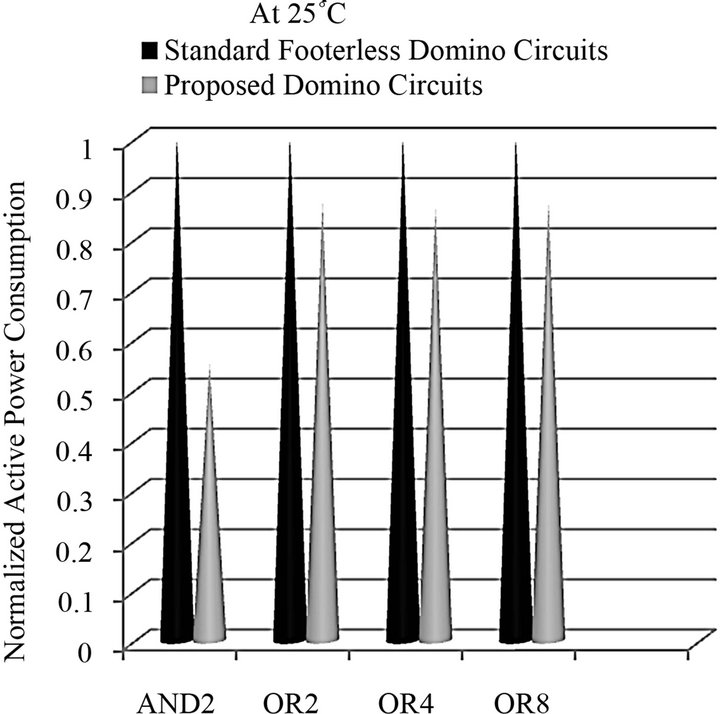
Figure 9. Active power consumption of two domino circuit techniques at 25˚C. For each circuit power consumption is normalized to the power consumed by standard footerless domino technique.
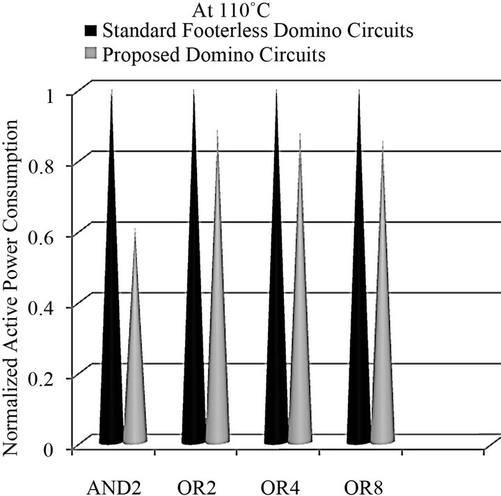
Figure 10. Active power consumption of two domino circuit techniques at 110˚C. For each circuit power consumption is normalized to the power consumed by standard footerless domino technique.
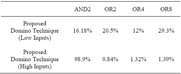
Table 1. Leakage power saving during ideal mode for low and high inputs at 25˚C compared with standard footerless domino circuits.
reduction varies from 0.84% to 98.9% as compared with standard footerless domino circuits. Based on the results, during idle mode at room temperature if low inputs are maintained very low leakage current will flow in the circuit except in AND2 circuit high inputs should be maintained for low leakage current.
4.3. Ideal Mode Leakage Power Consumption at 110˚C
Under same conditions as at 25˚C simulations are done for 110˚C. The leakage power reduction offered by the proposed circuit technique is listed in Table 2.
The proposed domino technique reduces the total leakage power 6.3% to 16.14% driven with low inputs and when driven with high inputs reduce the total leakage power by 0.064% to 98.6% as compared with standard footerless domino circuits. Same as in 25˚C if low inputs are maintained very low leakage current will flow in the circuit except in AND2 circuit high inputs should be maintained for low leakage current.
4.4. Non-Ideal Mode Leakage Power Consumption at 25˚C
In non-ideal mode the clock is low and precharge transistor is ON charging the dynamic node and the node voltage goes high. At the same time leakage current of the circuit depends on the input vectors applied at the input of the evaluation network. Based on the input conditions the circuits are simulated for the evaluation of the leakage current in non-ideal mode. In the first condition the inputs are low and in the second condition all the inputs are high. The inputs applied in the evaluation network will not put any effect on the voltage of dynamic node during non-ideal mode it will remain at the high voltage potential. The leakage power reduction offered by the proposed circuit technique is listed in Table 3. In nonideal mode at low temperature gate oxide leakage is more than the gate oxide leakage in ideal mode.
The proposed domino technique leads to the reduction of total leakage power by 31.79% to 92.55% driven with low inputs and 1.19% to 3.49% driven with high inputs when compared with standard footerless domino circuit.

Table 2. Leakage power saving during ideal mode for low and high inputs at 110˚C compared with standard footerless domino circuits.
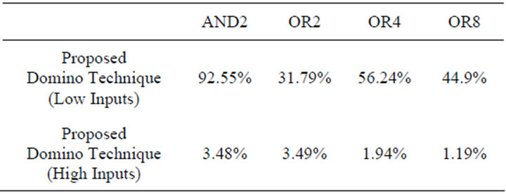
Table 3. Leakage power saving during non-ideal mode for low and high inputs at 25˚C compared with standard footerless domino circuits.
Based on the simulation result at room temperature if low inputs are maintained during non-ideal mode very low leakage current will flow in this circuit compared with high inputs.
4.5. Non-Ideal Mode Leakage Power Consumption at 110˚C
Based on same condition as non-ideal mode at 25˚C simulations are performed for 110˚C. The leakage power reduction offered by the proposed circuit technique is listed in Table 4.
The lector with footed diode inverter domino technique leads to the reduction of total leakage power by 6.35% to 85.77% driven with low inputs and 0.96% to 5.77% driven with high inputs when compared with standard footerless domino circuit. Same as in 25˚C if low inputs are maintained at high die temperature very low leakage current will flow in the circuits in comparison with high inputs.
5. Conclusions
In the 65 nm technologies both the gate dielectric and subthreshold leakage currents must be suppressed for reducing power consumption during idle and non-ideal mode. Therefore, a new domino technique is proposed for simultaneously reducing gate oxide and subthreshold leakage currents in domino logic circuits in same mode (ideal or non-ideal) with different input conditions.
The proposed domino circuit technique exploits the stacking effect employed between precharge and evaluation network. For further reducing the leakage power consumption a transistor in diode-footed configuration is introduced in the pull-down of the output inverter for better reduction of subthreshold and gate oxide leakage of the overall domino circuits. Result shows reduction of active power by 12.88% to 44.76% at low and 10.9% to 39.3% at high die temperatures. In ideal mode 0.84% to 98.9% and 0.064% to 98.6% reduction of leakage with low and high inputs at 25˚C and 110˚C respectively and in non-ideal mode 1.19% to 92.55% and 0.96% to 85.77% with low and high inputs at 25˚C and 110˚C respectively when compared with standard footerless dom-
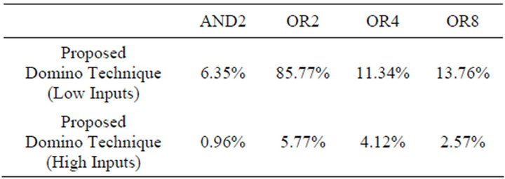
Table 4. Leakage power saving during non-ideal mode for low and high inputs at 110˚C compared with standard footerless domino circuits.
ino circuits. This technique can be used for very low power applications.
REFERENCES
- H. Mahmoodi-Meimand and K. Roy, “A Leakage-Tolerant High Fan-in Dynamic Circuit Style,” IEEE International Systems-on-Chip Conference, 17-20 September 2003, pp. 117-120. doi:10.1109/SOC.2003.1241475
- J.-S. Wang, S.-J. Shieh, C. Yeh and Y.-H. Yeh, “PseudoFootless CMOS Domino Logic Circuits for High-Performance VLSI Designs,” IEEE International Symposium on Circuits and Systems, Hiroshima, 25-28 July 2004, pp. 401-404.
- V. Kursun and E. G. Friedman, “Domino Logic with Variable Threshold Voltage Keeper,” IEEE Transactions on Very Large Scale Integration (VLSI) Systems, Vol. 11, No. 6, 2003, pp. 1080-1093.
- Y. Taur and T. H. Hing, “Fundamentals of Modern VLSI Devices,” Cambridge University Press, New York, 1998, pp. 120-128.
- K. Roy, et al., “Leakage Current Mechanisms and Leakage Reduction Techniques in Deep-Submicrometer CMOS Circuits,” IEEE Proceedings, Vol. 91, No. 2, 2003, pp. 306-327. doi:10.1109/JPROC.2002.808156
- Y. Taur and T. H. Hing, “Fundamentals of Modern VLSI Devices,” Cambridge University Press, New York, 1998, pp. 94-95.
- Y. Taur and T. H. Hing, “Fundamentals of Modern VLSI Devices,” Cambridge University Press, New York, 1998, pp. 97-99.
- K. Roy and S. C. Prasad, “Low-Power CMOS VLSI Circuit Design,” Wiley Interscience Publications, New York, 2000, pp. 28-29.
- K. Roy and S. C. Prasad, “Low-Power CMOS VLSI Circuit Design,” Wiley Interscience Publications, New York, 2000, pp. 27-28.
- Z. Liu and V. Kursun, “Leakage Power Characteristics of Dynamic Circuits in Nanometer CMOS Technologies,” Transactions on Circuits and Systems Part II—Express Briefs, Vol. 53, No. 8, 2006, pp. 692-696.
- H. Sasaki, M. Ono, T. Ohguro, S. Nakamura, M. Satio and Iwai, “1.5 nm Direct-Tuneling Gate Oxide Si MOSFETs,” IEEE Transactions on Electron Devices, Vol. 43, No. 8, 1996, pp. 1233-1242.
- F. Moradi and A. Peiravi, “An Improved Noise—Tolerant Domino Logic Circuit for High Fan-In Gates,” IEEE Proceedings, 2005, pp. 116-121.
- M. C. Johnson, D. Somasekhar, L. Y. Chiou and K. Roy, “Leakage Control with Efficient Use of Transistor Stacks in Single Threshold CMOS,” IEEE Transactions on Very Large Scale Integration Systems, Vol. 10, No. 1, 2002, pp. 1-5. doi:10.1109/92.988724
- S. Narendra, S. Borkar, V. De, D. Antoniadis and A. P. Chandrakasan, “Scaling of Stack Effect and Its Application for Leakage Reduction,” IEEE International Symposium on Low Power Electronics and Design, August 2001, pp. 195-200.
- S. Sirichotiyakul, T. Edwards, C. Oh, R. Panda and D. Blaauw, “Duet: An Accurate Leakage Estimation and Optimization Tool for Dual-Vt Circuits,” IEEE Transactions on Very Large Scale Integration Systems, Vol. 10, No. 2, 2002, pp. 79-90. doi:10.1109/92.994980

