Engineering
Vol.4 No.8(2012), Article ID:22170,3 pages DOI:10.4236/eng.2012.48064
Fast CR-SRAM Using New Charge-Recycling Scheme
1School of Electronics and Information, Tongji University, Shanghai, China
2School of Microelectronics, Shanghai Jiao Tong University, Shanghai, China
Email: 0952080012@tongji.edu.cn, wangxu@ic.sjtu.edu.cn
Received June 5, 2012; revised July 2, 2012; accepted July 15, 2012
Keywords: SRAM; lower-power; Charge-recycling
ABSTRACT
In this paper, a CR-SRAM using new charge recycling scheme is described, novel bit-line pre-charge voltage distribution is proposed. The SRAM pre-charge voltage level is designed by logarithm instead of linear. The new design leads to improvement in speed compared to the original CR-SRAM. Simulation results show that the new CR-SRAM using novel pre-charge voltage distribution scheme reduced the write access time by 34% with 9% power dissipation penalty.
1. Introduction
As the demands for handheld devices and other battery-supplied equipments increase, more and more attention has been paid on low power IC design. SRAM takes a large power dissipation of the whole chip. Many low power SRAMs has been designed [1]. One important way to reduce SRAM power dissipation is reducing the power consumed by bit-line. During write and read operation, the bit-line voltage swing is full, charging and discharging of the highly capacitive bit-lines consumes a lot of energy.
Reducing the bit-line power consumption during write cycle is an effective way to reduce the power dissipation. Recently, a low power using bit-line charge-recycling technology has been reported [2]. The charge recycling concept was firstly introduced in the low power on-chip bus architecture design [3], B. D. Young apply this technology to ROM [4]. Kim applied charge-recycling directly to the bit-line to reduce dynamic write power associated with bit-line swing in SRAM [1]. The main idea of this technique is that the charge stored in the bit-line during one write cycle can be recycled for the next write operation, which leads to reduction of power dissipation to 1/N2, while N is the bit-line pair number.
However, the original CR-SRAM has two disadvantages. Firstly, the access time of write operation is long, the operation frequency is limited. Secondly, when the recycle time increase, the voltage interval began to getting small, which lead to SNM decrease when the recycling time rise.
In this paper, a new charge-recycling scheme is proposed to further enhance the performance and stability of CR-SRAM. The logarithmic pre-charge voltage is applied to write operation. To verify the new charge recycling scheme, a prototype 2 Kbits Charge-Recycling SRAM is implemented and simulated in SMIC 0.13 μm CMOS technology. The simulate results exhibit the write speed is 34% faster than original design. The average power dissipation per write cycle is 2.4 μW at 1.5 V supply.
The rest of the paper is organized as follows: In section II, the new charge recycling scheme is introduced. In section III, a prototype 2 Kbits SRAM using the new charge-recycling scheme is built and simulated, the performance of new CR-SRAM is also analyzed.
2. New Charing Recycling Scheme
The proposed new charge recycling scheme is that the pre-charge voltage distribution is logarithmic instead of linear. The pre-charge voltage is given by the following function.
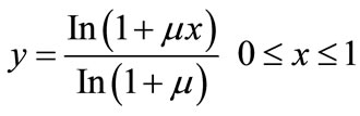 (1)
(1)
Equation (1) is used in Pulse Code Modulation as an unequal quantization method in the area of communication. The μ is called compression factor. The μ law function is illustrated in Figure 1. When μ = 0, the function is linear. When μ increase, the curves are more apart from linear. The function is odd symmetry.
The new pre-charge voltage is calculated as follow. Firstly, determine the compression factor μ and chargerecycling bit-line pair number N. Secondly, divide the supply voltage range into tow parts, 0 to VDD/2 and VDD/2 to VDD. In the VDD/2 to VDD range, replace y axes range with VDD/2 to VDD, calculated the voltage value by

Figure 1. μ law bit-line voltage.
x equal 1/2 and 3/4, In the range 0 to VDD/2, the voltage value is calculated similarly. When the charge-recycling bit-line pair number N is 4, and μ = 1, the pre-charge voltages is 1.41 V, 1.19 V, 0.40 V, 0.17 V.
When the pre-charge voltages is determined, mapping each voltage level to SRAM circuit through corresponding resistors. In the proposed SRAM illustrated in Figure 2, the corresponding resistors are R1 to R5.
This CR-SRAM using new pre-charge scheme has two advantages compared to the original CR-SRAM, the write speed is improved and the static noise margin is increased.
2.1. Imporve the Write Speed
The write speed is limited by the time which taken by the maximum voltage of bit-line increased to VDD. As is showing in Figure 3, the maximum voltage level is V1, which is 1.31 V. The bit-line is charged by supply VDD, the voltage change is slow compared to other bit-line pairs. The circumstance is same as V4, which is discharged by source-line VSS. V1 and V4 take the longest time since that the bit-line is connected to source-line while the other bit-line pair are charge and discharged by the parasitical capacitors. When the bit-line voltage level is designed according to (1), the time consumed by the V1 charged to VDD is short since the voltage is higher than the original V1, which is same as V4, the voltage is lower than original. The logarithmic voltage design makes the time consumed by the bit-line pairs in evaluate phase more equally, and consequently lead to write speed improvement.
2.2. Increase SRAM Static Noise Margin
Another advantage is the SNM is not decreased crucially when the charge recycling time increase. The original bit-line pre-charge voltage level is given by (2).
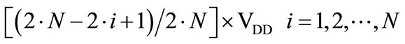 (2)
(2)
For N = 4, according to (2), the pre-charge voltage are 0.19 V, 0.56 V, 0.91 V, 1.31 V. The bit-line voltage is decreased due to the charge leakage in write cycle. Every time the charge recycled for one write operation, the voltage decreased after the bit-line pair connected to evaluate, which lead to the voltage margin in the last few
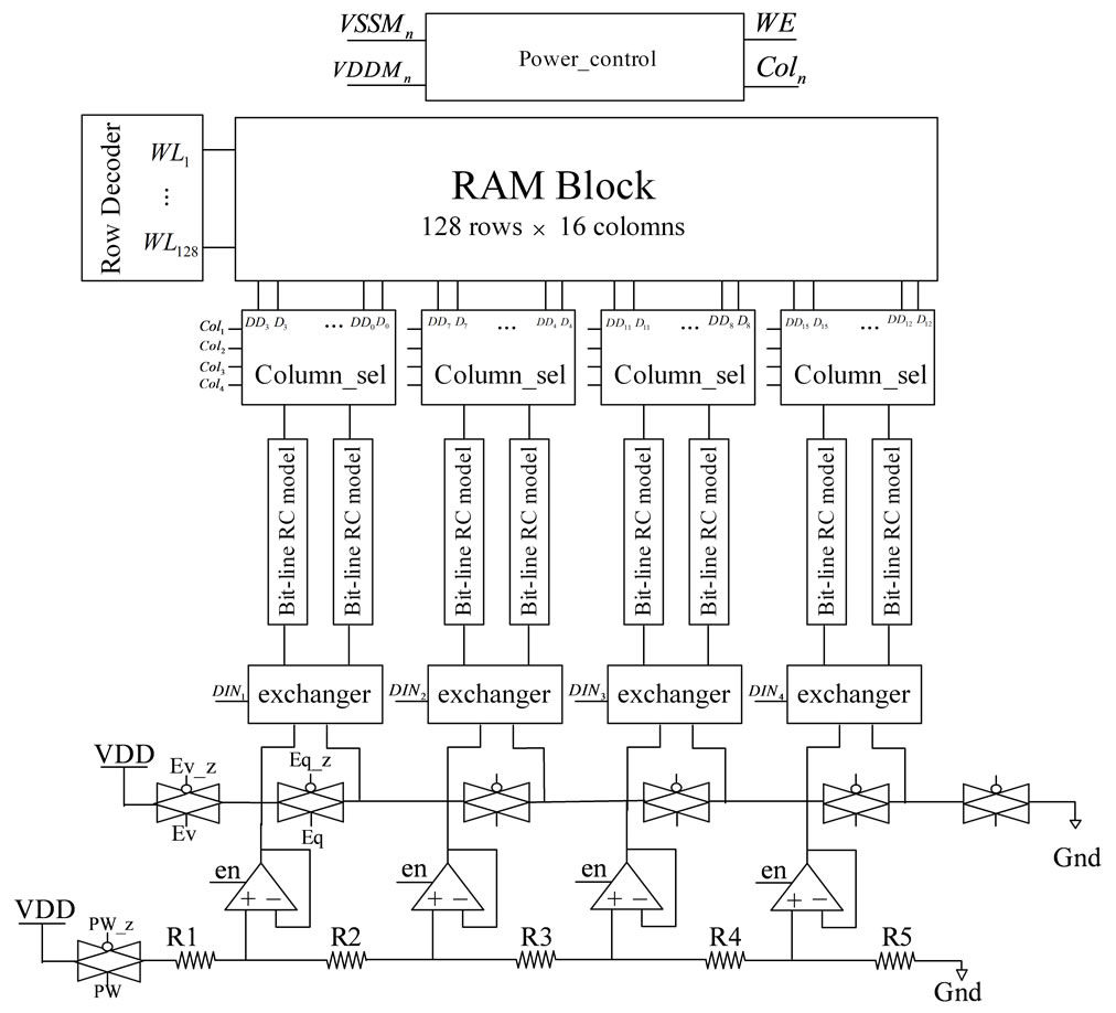
Figure 2. CR-SRAM architecture using new pre-charge voltage distribution scheme.
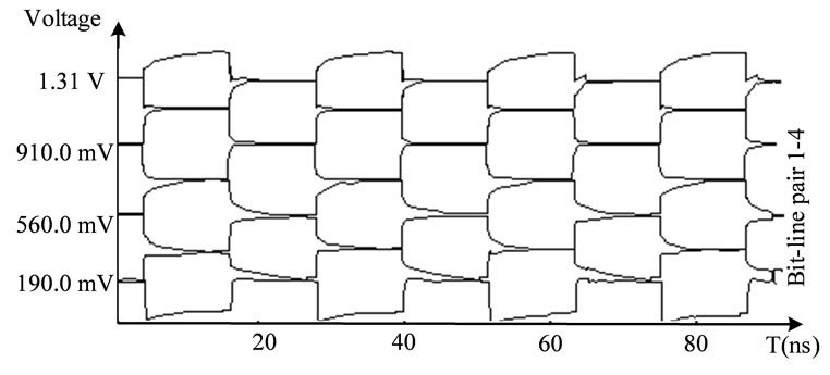
Figure 3. Simulated waveform of original CR-SRAM.
write cycle getting small. The SNM of SRAM is limited by the smallest voltage difference of the last write cycle.
3. SRAM Simulation and Results
To demonstrate the concept of the proposed chargerecycling scheme, a 2 K bits CR-SRAM has been designed and simulated in SMIC 0.13 μm CMOS technology. As is showing in Figure 2, the main blocks are illustrated below.
• The exchanger block is used by bit-line pair for charge-recycling. If the number of exchangers is N, the charge will recycled for N times.
• The Bit-line RC model block is a π RC model of electronic wire. The values of capacitors and resistors are determined by the technology file provided by the Fab.
• To make data write in SRAM cells correctly, the power control block is dedicated to floating the source line during write operation. The source line VDD and VSS are disconnected from the RAM Cell to ensure data write in with limited bit-line voltage [5]. During SRAM data retention period, VSS is connected to positive bias voltage to reduce power dissipation.
• The pre-charge circuit is implemented by a unit gain buffer which has rail-to-rail swing. To enhance output voltage swing, complementary PMOS and NMOS difference amplifier is used.
During simulation, the control signals are provided to generate four consecutive write operations, which consist a charge-recycling cycle. The simulated waveforms of original and proposed CR-SRAM are show in Figures 3 and 4.
From the simulated waveforms of proposed CRSRAM and original CR-SRAM, the write speed of new CR-SRAM is improved 34% compared to the original one. Meanwhile, the power dissipation of new CRSRAM is 2.4 μW, and the original CR-SRAM consumes
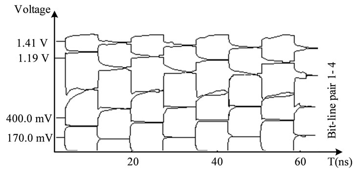
Figure 4. Simulated waveform of proposed CR-SRAM.
2.2 μW per write access, the power dissipation is increased about 9%. Besides, the original CR-SRAM bitline voltage margin shrink due to charge leakage, the bitline voltage margin of proposed CR-SRAM is enhanced.
4. Conclusion
Recycling the charge of bit-line for multiple write operation is an effective way to decrease SRAM power dissipation. CRSRAM can reduce the power dissipation to 1/N2. The logarithmic pre-charge voltage is proposed to further optimize write speed. According to simulated results, the write speed is improved by 34%, while the power dissipation increased 9%.
REFERENCES
- K. Keejong, H. Mahmoodi and K. Roy, “A Low-Power SRAM Using Bit-Line Charge-Recycling,” IEEE Journal of Solid-State Circuits, Vol. 43, No. 2, 2008, pp. 446-459. doi:10.1109/JSSC.2007.914294
- B.-D. Yang, “A Low-Power SRAM Using Bit-Line ChargeRecycling for Read and Write Operations,” IEEE Journal of Solid-State Circuits, Vol. 45, No. 10, 2010, pp. 2173- 2183. doi:10.1109/JSSC.2010.2063950
- H. Yamauchi, H. Akamatsu and T. Fujita, “An Asymtotically Zero Power Charge-Recycling Bus Architecture for Battery-Operated Ultrahigh Data Rate ULSI’s,” IEEE Journal of Solid-State Circuits, Vol. 30, No. 4, 1995, pp. 423- 431. doi:10.1109/4.375962
- B. D. Yang and L. S. Kim, “A Low Power Charge-Recycling ROM Architecture,” IEEE Transactions on Very Large Scale Integration (VLSI) Systems, Vol. 11, No. 4, 2003, pp. 590-600.
- M. Yamaoka, N. Maeda, Y. Shinozaki, K. Nii, S. Shimada, K. Yanagi-sawa and T. Kawahara, “90-nm Process-Variation Adaptive Embedded SRAM Modules with Power-Line-Floating Write Technique,” IEEE Journal of Solid-State Circuits, Vol. 41, No. 3, 2006, pp. 705-711. doi:10.1109/JSSC.2006.869786