Materials Sciences and Applications
Vol.4 No.9(2013), Article ID:36867,8 pages DOI:10.4236/msa.2013.49069
Mechanical Properties of Composite SiNx/DLC Films Prepared by Filtered Cathodic Arc of Graphite Incorporated with RF Sputtering of Silicon Nitride
![]()
1Department of Physics, Faculty of Science, King Mongkut’s University of Technology Thonburi, Bangkok, Thailand; 2Western Digital (Thailand) Co., Ltd., Ayutthaya, Thailand; 3Thailand Center of Excellence in Physics, CHE, Ministry of Education, Bangkok, Thailand
Email: *opticslaser@yahoo.com, *Phuwanai.Bunnak@wdc.com
Copyright © 2013 P. Bunnak et al. This is an open access article distributed under the Creative Commons Attribution License, which permits unrestricted use, distribution, and reproduction in any medium, provided the original work is properly cited.
Received July 18th, 2013; revised August 19th, 2013; accepted August 27th, 2013
Keywords: Silicon Nitride; Diamond-Like Carbon; Composite SiNx/DLC Film; Filtered Cathodic arc
ABSTRACT
Composite SiNx/DLC films were deposited on Si substrate by RF magnetron sputtering of silicon nitride (Si3N4) target simultaneously with filtered cathode arc (FCA) of graphite. The RF power was fixed at 100 W whereas the arc currents of FCA were 20, 40, 60 and 80 A. The effects of arc current on the structure, surface roughness, density and mechanical properties of SiNx/DLC films were investigated. The results show that the arc current in the studied range has effect on the structure, surface roughness, density and mechanical properties of composite SiNx/DLC films. The composite SiNx/DLC films show the sp3 content between 53.5% and 66.7%, density between 2.54 and 2.98 g/cm3, stress between 1.7 and 2.2 GPa, and hardness between 35 and 51 GPa. Furthermore, it was found that the density, stress and hardness correlate linearly with the sp3 content for composite SiNx/DLC films.
1. Introduction
Diamond-like carbon (DLC) film has many attractive properties, such as high hardness, high wear resistance, high corrosion resistance, low friction coefficient, chemical inertness to both acids and alkalis and lack of magnetic response [1-5]. In past years, DLC films have been extensively used for tribological application in many areas, such as mechanical parts, optical devices, magnetic storage disks and biomedical parts [6-9]. In current hard disk drive technology, DLC films have been used as protective overcoat on the head and disk surfaces in magnetic storage devices [10-12]. The DLC film behaves as a barrier to prevent the head and magnetic media against wear and corrosion [12,13]. Various techniques have been used for the deposition of DLC films. However, the filtered cathodic vacuum arc (FCVA) has been proved to be the most promising technique for the deposition of high quality DLC films with sp3 contents of more than 80% and results in high hardness and chemical inertness [12,14-18].
However, DLC has low adhesive bond strength to metal surface; in the magnetic storage industry to improve the adhesions strength, amorphous silicon (a-Si) seed layer is firstly deposited on the metal substrate before depositing of the DLC film on top of it. Liu et al. [19], and Liu and Wang [20] reported the coating of Si layer with a thickness of 1 nm on the substrate as a seed layer before coating DLC film. Recently, different amorphous Si based films such as a-Si, a-SiNx, a-SiCx and a-SiCx Ny were studied as the underlayers of DLC by Azzi et al. [21]. They reported that a-SiNx/DLC film exhibited the most promising combination. Consequently, Wang et al. [18] reported silicon nitride (Si-Ni) gradient films prepared by nitriding of Si thin films as the underlayer of DLC film.
In present study, composite SiNx/DLC films were deposited on Si substrates by RF magnetron sputtering of Si3N4 target simultaneously with FCA of graphite. The effects of arc current in FCA source on the structure, surface roughness, density and mechanical properties of the composite SiNx/DLC film were investigated.
2. Material and Methods
2.1. Deposition System
Figure 1 shows the schematic of deposition system used in this work. The system consists of load lock and process chambers. Each chamber has its own turbo molecular pump to evacuate the chamber to high vacuum individually. The pressure in each chamber was measured by ionization gauge. The load lock chamber was used to load and transfer the sample into the process chamber using magnetic couple transfer arm. Before opening the isolation valve and transfer the sample into the process chamber, the pressure in both chambers must be lower than 5 × 10⁻⁵ Torr. The process chamber equipped with RF magnetron sputtering source with 6 inch in diameter and 99.99% purity silicon nitride (Si3N4) as a sputtering target, and filtered cathodic arc (FCA) of graphite with double bend magnetic solenoid filter including 99.999% purity graphite with a diameter of 2 inch and a length of 4 inch.
The base pressure of the system prior to the deposition was less than 5 × 10⁻⁷ Torr. Ar gas was used as a sputtering gas. The process pressure was controlled by automatic pressure controller (APC). The Ar gas flow and pressure can be set in software, and then process pressure was measured by a capacitance manometer gauge and feed back to APC. The APC valve can be adjusted to a required pressure set point. Si (100) with a diameter of 2 inch was used as a substrate. The substrate holder has features of tilt, rotation and bias capabilities.
2.2. Films Preparation
For the deposition of composite SiNx/DLC films, SiNx and DLC films were deposited simultaneously on Si substrates using RF magnetron sputtering of Si3N4 target and filtered cathodic arc of graphite, respectively. The RF power was fixed at 100 W whereas the arc currents of
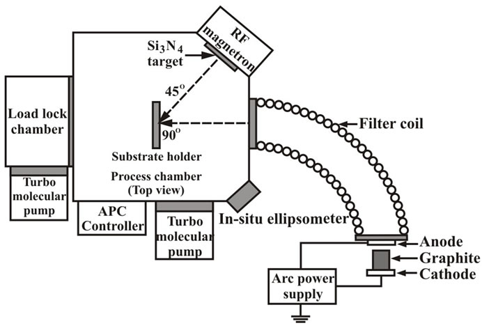
Figure 1. Schematic of deposition system.
FCA were 20, 40, 60 and 80 A. All the experiments were performed at an argon gas flow rate of 3 sccm and a process pressure was controlled by automatic pressure control valve at 0.6 mTorr. The substrate was tilted normal to FCA source. Thus, it was perpendicular to the carbon plasma direction and 45 degree to Si3N4 target. Films with a thickness of approximately 10 nm were prepared for the characterization of surface morphology, structure and film density. In addition, films with a thickness of approximately 50 nm were prepared for mechanical properties analysis such as film stress, hardness and wear resistance. The film thickness was controlled by specific deposition time based on deposition rate of each condition. The rotation speed of the substrate holder was set at 15 rpm to improve thickness uniformity of deposited films.
2.3. Characterization
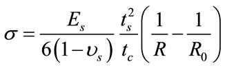
The structure of composite SiNx/DLC films was investtigated by Raman spectroscopy using a Renishaw inVia Reflex Raman spectrometer at 514 nm in back scattering geometry. The 514 nm obtained from an argon ion laser with a laser output of 20 mW and 50× objective lens were used, which resulted in an incident power at the sample surface of approximately 4 mW. Raman shifts were measured in a frequency range from 1150 to 1900 cm−1, with 1 cm−1 resolution. The raw Raman spectra were fitted using Gaussian profile to obtain smooth curves. Then, the smooth curves were fitted using two Gaussian profiles corresponding to G peak and D peak [22].
The fraction of sp3 bonding in the film was determined using electron energy-loss spectroscopy (EELS). The EELS spectra were acquired at 200 kV using FEI Tecnai Osiris scanning transmission electron microscope (STEM) equipped with a Gatan GIF Quantum SE imaging filter which is able to excel both as an imaging filter and a high performance EELS spectrometer with a 2.5 mm EELS entrance aperture.
The surface morphology and roughness of composite SiNx/DLC films and pure DLC films were investigated by atomic force microscopy (AFM, Park System XEPTR), operating in tapping mode. The thickness of the films was determined by step height measurement between film and substrate, created by resist-pen lifting. An AFM height histogram, averaging over 10 µm × 5 µm scanning area. The 3 µm × 3 µm area over the films was used for surface roughness (Ra) calculation.
X-ray reflectivity (XRR) is a non-destructive method and widely used to determine the density and thickness of thin films [23]. XRR was performed using a Philips X’ Pert MRD diffractometer with a Cu target X-ray tube operated at 45 kV and 40 mA. The reflected X-ray intensity was recorded at the grazing incident angle from 0˚ to 5˚ with a step of 0.0080˚. The incident optics was a 10-mm incident beam mask and a 1/32˚ divergence slit. The receiving optic was a 0.27˚ parallel-plate collimator with 0.1-mm fine slit.
The intrinsic stress in the deposited film is generally compressive due to the generation of sp3 bond. The surface profilometer (KLA Tencor, P16+) was used to determine the film stress by measuring the radius of curvature of bare silicon substrate and the substrate with deposited films. Then, the stress  in a thin film of thickness tc is determined by Stoney’s equation [24]
where Es, υs, and ts are the Young’s modulus, Poisson ratio and thickness of the substrate. R0 and R are radii of curvature of the bare substrate and film-substrate composite, respectively.
The nanoindentater (Hysitron, Triboindentor) was used to measure the hardness and wear resistance. The hardness is defined as the indentation load divided by projecttion contact area of the indentater [25]. The cube corner tip probe with 45 nm radius of curvature was used for hardness measurement. For wear resistance test, the cube corner tip probe with 100 nm radius of curvature was used with apply constant normal load 8 mN to create a wear pattern area of 2 mm ´ 2 mm with two passes scan. The wear region was examined using a scanning probe microscope (SPM) with an area of 5 mm ´ 5 mm to cover the wear pattern area and the wear depth was measured. The higher wear depth means the lower wear resistance and hence more material removed for a given force.
3. Results and Discussion
3.1. Raman Spectroscopy
Figure 2 shows the visible Raman spectra from 1150 to 1900 cm−1 of composite SiNx/DLC films deposited at various (FCA) arc currents. In order to have further understanding of Raman spectra, these Raman spectra were fitted with two Gaussian profiles corresponding to G peak at around 1570 cm−1 and D peak at around 1435 cm−1, respectively.
Table 1 shows the G-peak position, D-peak position and ID/IG ratio extracted from the Raman spectra. It was observed that the G-peak position shifted towards higher frequencies and the ID/IG ratio decreases with increasing arc current. Because the increase of arc current results in the increase of carbon ion generated from the carbon source while SiNx generated from the Si3N4 target remains constant. As a result, the concentration of DLC in composite SiNx/DLC films increases and hence the degree of disorder (ID/IG ratio) decreases and a shift in G-peak position towards higher frequencies. This is due to the incorporation of SiNx cause the open up of sp2 ring and the sp2 cluster size was reduced [26]. Therefore, sp3 content increases with increasing arc current. This result is confirmed by the direct determination of sp3 content using EELS. The values of the sp3 content in composites SiNx/DLC films are shown in Table 1. It is seen that the sp3 content increases from 53.5% at arc current 20 A to a maximum of 66.7% at arc current 80 A.
3.2. Surface Morphology
Figure 3 shows the typical AFM images obtained from the step height and surface morphology of composite SiNx/DLC films. As can be seen from the step height of AFM images, all the composite SiNx/DLC films have the same thickness of 10 nm. Table 2 shows the roughness of composite SiNx/DLC films. The surface morphology of the films reveals that the film surface is very smooth. The roughness of all the composite SiNx/DLC films is almost constant in the range of 0.15 - 0.17 nm. This is due to the Si substrates used for the deposition of the films are of polished grade wafers with a surface roughness of about 0.07 nm. The above result indicates that the arc current in this study range has little effect on the surface morphology of composite SiNx/DLC films.
3.3. XRR
The detail on the XRR theory has been described by Ferrari et al. [23]. The X-ray refractive index of a
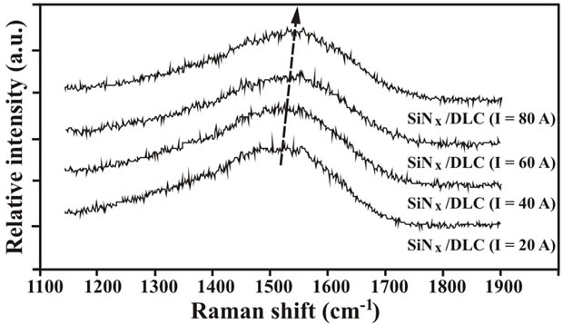
Figure 2. Raman spectra of composite SiNx/DLC films.

Table 1. Information extracted from Raman spectra of composite SiNx/DLC films.
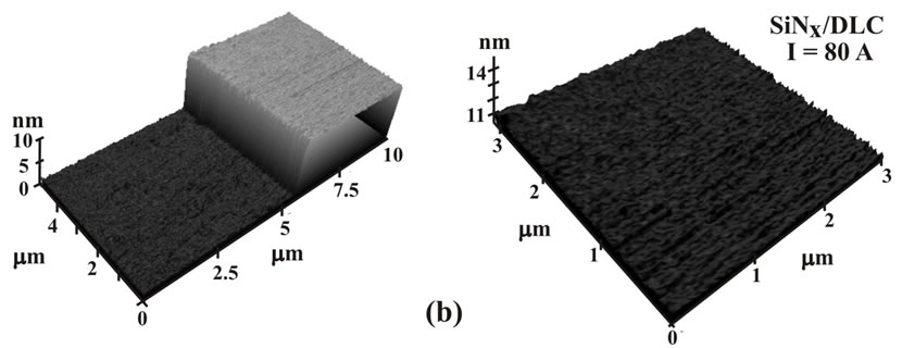
Figure 3. AFM images showing step height (left-hand side) and surface morphology (right-hand side) of composite SiNx/DLC films deposited at the arc currents of: (a) 20 A and (b) 80 A.
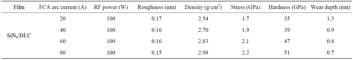
Table 2. Roughness, density, compressive stress, hardness and wear depth of composite SiNx/DLC films.
material is slightly less than 1, so that total external reflection occurs at low angles of incidence. As the incident angle  increases above a critical angle
 , Xray begin to penetrate into the film. Applying Snell’s law at the air/film interface, the critical angle can be derived and used to calculate overall mass density of the film. For diamond,
  is 0.245˚ at l = 1.39 Å. This direct method that use the critical angle to determine the film density is uncertain for some films such as ta-C:H because the obtained density is equal or smaller than that of Si substrate density (2.33 g/cm3). Hence, the value of critical angle as determined by this method is the critical angle value of Si and not that of the film [10].
Figure 4 shows the typical X-ray reflectivity curve obtained from composite SiNx/DLC films. For thin layer on substrate, the interference between X-ray scattered from the air/film and the film/substrate interfaces create a fringe period on the reflectivity curve and the period of this oscillation is directly related to the thickness of the film [27].
In this work, the simulation software (X’Pert reflectivity) was used to analyze the film density. Base on the model, the reflectivity curve is simulated and then com-
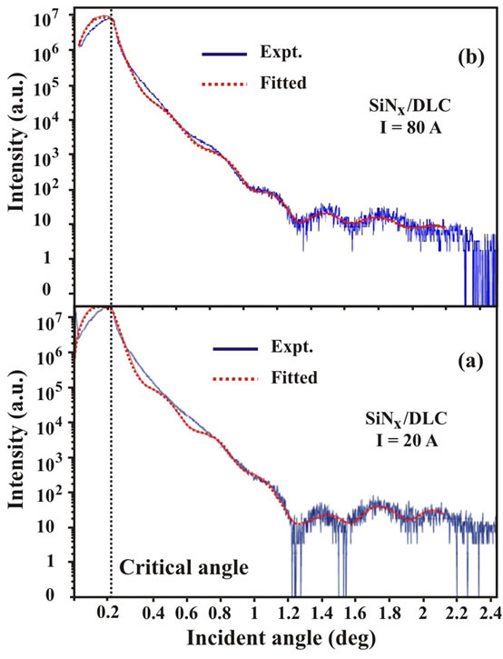
Figure 4. X-ray reflectivity curve obtained from composite SiNx/DLC films deposited at the arc currents of: (a) 20 A and (b) 80 A.
pared with the measured data using a genetic algorithm method until the right combination of layer thickness, roughness and density minimizes the error function (E) defined as [28]
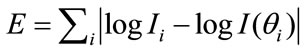
where Ii and  are the experimental and simulated intensity values at the incident angle
  . The summation is taken over all point i in the reflectivity curve.
The density of the films obtained from the X-ray reflectivity curves in Figure 4 are summarized in Table 2. It was found that the density increases from 2.54 to 2.98 g/cm3 as the arc current was increased from 20 to 80 A. The density 2.98 g/cm3 at an arc current of 80 A is slightly less than that of diamond (3.51 g/cm3).
3.4. Film Stress
The compressive stress values of composite SiNx/DLC films are given in Table 2. It is clearly observed that the
compressive stress increases from 1.7 to 2.2 GPa as the arc current is increased from 20 to 80 A, The increase of compresive stress in composite SiNx/DLC film is due to the change in the film microstructure. Holmberg et al. [29] reported that the compressive stresses in vacuumdeposited coating are related to the microstructure and thus sensitive to the deposition condition.
3.5. Hardness and Wear Resistance
The hardness of composite SiNx/DLC films is given in Table 2. It is seen that the hardness of composite SiNx/DLC films increases from 35 to 51 GPa as the arc current is increased from 20 to 80 A.
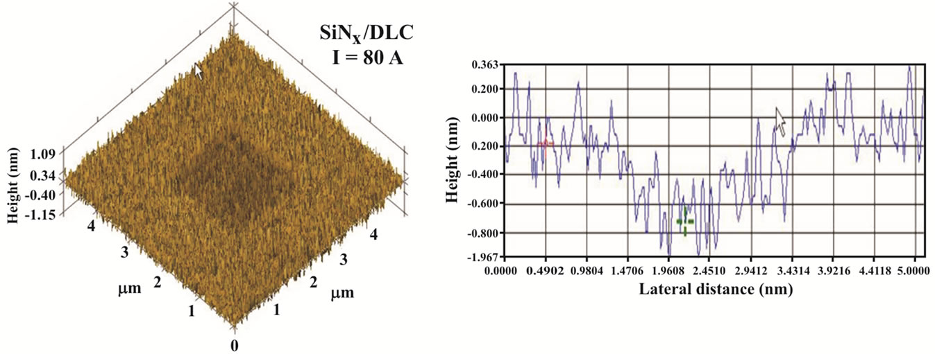
Figure 5 shows the SPM images of the films with a probing area of 55 mm ´ 5 mm and a wear pattern area of 2 mm ´ 2 mm. The left-hand side picture is the 3D image. The right-hand side picture is the cross-sectional image showing the depth profile and the wear depth is determined. The wear depth values of composite SiNx/DLC
 (a)
(a)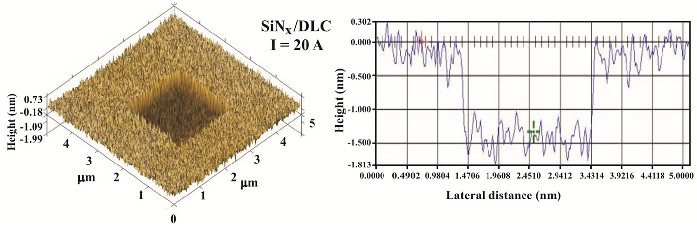 (b)
(b)
Figure 5. SPM images showing 3D image of the probing area of 55 mm ´5 mm and a wear pattern area of 25 mm ´ 2 mm (left-hand side) and dept profile (right-hand side) of composite SiNx/DLC films deposited at the arc currents of : (a) 20 A and (b) 80 A.
films are given in Table 2. It is seen that the wear depth value decreases from 1.3 to 0.7 nm as the arc current is increased from 20 to 80 A.
The results on the effect of arc current on ths sp3 content, density, stress, hardness and wear depth of the composite SiNx/DLC films are presented in Figure 6. It is clearly observed that in present study the arc current in the range of 20 to 80 A has effect on the mechaincal properties of the films. The density, stress and hardness of composite SiNx/DLC films was found to increase with incrasing arc current. The relation between density, stress, hardness, and wear depth and sp3 content was further investigated. Figure 7 shows the plots of density, stress, hardness and wear depth as a function of the sp3 content. It is seen that the density, stress and hardness vary in a similar way, as they all correlate directly with sp3 content. This is in good agreement with previous works as repoted in Ref. [10].
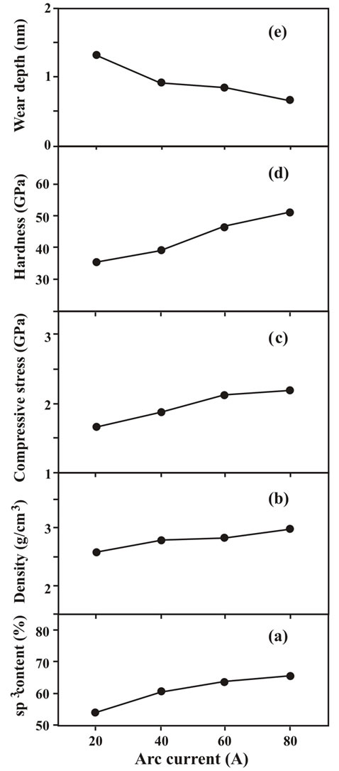
Figure 6. Variations of: (a) sp3 content, (b) density, (c) compressive stress, (d) hardness and (e) wear depth as a function of the arc current for composite SiNx/DLC films deposited at various arc currents of 20, 40, 60 and 80 A.
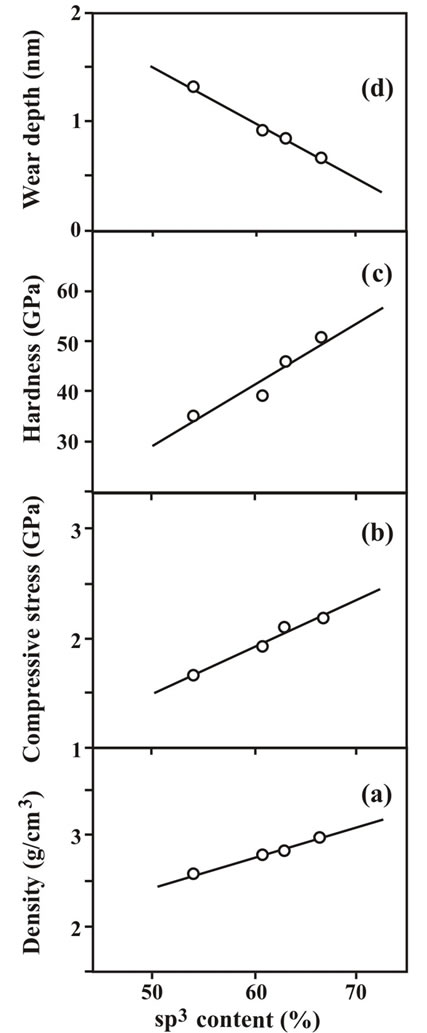
Figure 7. Variatons of: (a) density, (b) compressive stress, (c) hardness and (d) wear depth as a function of the sp3 content for compsited SiNx/DLC films.
4. Conclusion
Composite SiNx/DLC films were prepared from the RF magnetron sputtering of Si3N4 target and together with filtered cathodic arc of graphite. During the deposition, the RF power was maintained at 100 W while the arc current of graphite was varied from 20 to 80 A. The results show that the sp3 content, density, stress and hardness of composite SiNx/DLC films increase with increasing arc current in the studied range. The composite SiNx/DLC films show sp3 content between 53.5 and 66.7%, density between 2.54 and 2.98 g/cm3, stress between 1.7 and 2.2 GPa, and hardness between 35 and 51 GPa. Furthermore, it was found that the density, stress and hardness correlate linearly with the sp3 content. The above values of sp3 content, density, stress and hardness are considered to be high enough for slider overcoat in hard disk drive industry
5. Acknowledgements
This work was supported by Western Digital Thailand, Thailand Center of Excellence in Physics (ThEP) and King Mongkut’s University of Technology Thonburi under The National Research University Project
REFERENCES
- B. Bhushan, “Chemical, Mechanical and Tribological Characterization of Ultra-Thin and Hard Amorphous Carbon Coatings as Thin as 3.5 nm: Recent Developments,” Diamond and Related Materials, Vol. 8, No. 11, 1999 pp. 1985-2015. doi:10.1016/S0925-9635(99)00158-2
- S. Zhang, Y. Fu, H. Du, X. T. Zeng and Y. C. Liu, “Magnetron Sputtering of Nancomposite (Ti,Cr)CN/DLC Coatings,” Surface & Coatings Technology, Vol. 162, No. 1, 2002, pp. 42-48. doi:10.1016/S0257-8972(02)00561-3
- N. Paik, “Raman and XPS Studies of DLC Films Prepared by a Magnetron Sputter Type Negative Ion Source,” Surface & Coatings Technology, Vol. 200, No. 7, 2005, pp. 2170-2174. doi:10.1016/j.surfcoat.2004.08.073
- X. Yu, C.-B. Wang, Y. Liu and D.-Y. Yu, “A Study of Hard Diamond-Like Carbon Films in Mid-Frequency Dual-Magnetron Sputtering,” Diamond and Related Materials, Vol. 15, No. 9, 2006, pp. 1223-1227. doi:10.1016/j.diamond.2005.09.040
- A. S. Hamdy, “Electrochemical Behavior of DiamondLike-Carbon Coatings Deposited on AlTiC(Al2O3+TiC) Ceramic Composite Substrate in HCL Solution,” Electrochimica Acta, Vol. 56, No. 3, 2011, pp. 1554-156. doi:10.1016/j.electacta.2010.11.021
- J. Robertson, “Diamond-Like Amorphous Carbon,” Materials Science and Engineering R, Vol. 37, No. 4-6, 2002, pp. 129-281. doi:10.1016/S0927-796X(02)00005-0
- W. G. Cui, Q. E. Lai, L. Zhang and F. M. Wang, “Quantitative Measurements of sp3 Content in DLC Films with Raman Spectroscopy,” Surface & Coatings Technology, Vol. 205, No. 7, 2010, pp. 1995-1999. doi:10.1016/j.surfcoat.2010.08.093
- R. Crombez, J. McMinis, V. S. Veerasamy and W. Shen, “Experimental Study of Mechanical Properties and Scratch Resistance of Ultra-Thin Diamond-Like-Carbon (DLC) Coatings Deposited on Glass,” Tribology International, Vol. 44, No. 1, 2011, pp. 55-62. doi:10.1016/j.triboint.2010.08.004
- M. Fujii, M. A. Kumar and A. Yoshida, “Influence of DLC Coating Thickness on Tribological Characteristics under Sliding Rolling Contact condition,” Tribology International, Vol. 44, No. 10, 2011, pp. 1289-1295. doi:10.1016/j.triboint.2010.07.005
- A. C. Ferrari, “Diamond-Like Carbon for Magnetic Storage Disk,” Surface & Coatings Technology, Vol. 180- 181, 2004, pp. 190-206. doi:10.1016/j.surfcoat.2003.10.146
- C. Casiraghi, J. Robertson and A. C. Ferrari, “DiamondLike Carbon for Data and Beer Storage,” Materials Today, Vol. 10, No. 1-2, 2007, pp. 44-53. doi:10.1016/S1369-7021(06)71791-6
- M. Zhong, C. Zhang, J. Luo and X. Lu, “The Protective Properties of Ultra-Thin Diamond Like Carbon Films for High Density Magnetic Storage Devices,” Applied Surface Science, Vol. 256, No. 1, 2009, pp. 322-328. doi:10.1016/j.apsusc.2009.08.023
- C. Casiraghi, A.C. Ferrari, R. Ohr, D. Chu and J. Robertson, “Surface Properties of Ultra-Thin Tetrahedral Amorphous Carbon Films for Magnetic Storage Technology,” Diamond and Related Materials, Vol. 13, No., 2004, pp. 1416-1421. doi:10.1016/j.diamond.2003.10.086
- B. Druz, Y. Yevtuknov and I. Zaritsky, “Diamond-Like Carbon Overcoat for TFMH Using Filtered Cathodic Arc System with Ar-Assisted Arc Discharge,” Diamond and Related, Vol. 14, No. 9, 2005, pp. 1508-1516. doi:10.1016/j.diamond.2005.04.007
- G. G. Wang, H. Y. Zhang, H. F. Zhou, X. P. Kuang, Q. B. Wu, H. B. Zuo, J. C. Han and H. T. Ma, “Effect of ECR Assisted Microwave Plasma Nitriding Treatment on the Microstructure Characteristics of FCVA Deposited Ultra-Thin ta-C Films for High Density Magnetic Storage Application,” Applied Surface Science, Vol. 256, No. 10, 2010, pp. 3024-3030. doi:10.1016/j.apsusc.2009.11.067
- P. Siemroth, J. Berthold, B. Petereit and H. Schneider, “Hilgers, A New Generation of Filtered Arc Sources for Ultrathin Top Coats on Magnetic Hard Disks,” Surface & Coatings Technology, Vol. 188-189, 2004, pp. 684-690. doi:10.1016/j.surfcoat.2004.07.004
- H. Tanoue, M. Kamiya, S. Oke, Y. Suda, H. Takikawa, M. Taki, N. Tsuji, T. Ishikawa, H. Yasui, S. Temei and H. Takahashi, “Effect of Gas Introduction Position on Substrate Etching by Means of Ar-Dominated Graphite-Cathodic-Arc Plasma Beam in mT-FAD,” Thin Solid Films, Vol. 518, No. 13, 2010, pp. 3546-3550. doi:10.1016/j.tsf.2009.11.050
- G. G. Wang, X. P. Kuang, H. Y. Zhang, C. Zhu, J. C. Han, H. B. Zuo and H. T. Ma, “Silicon Nitride Gradient Film as the Underlayer of Ultra-Thin Tetrahedral Amorphous Carbon Overcoat for Magnetic Recording Slider,” Materials Chemistry and Physics, Vol. 13, No. 1-2, 2011, pp. 127-131. doi:10.1016/j.matchemphys.2011.07.077
- F. X. Liu, K. L. Yao and Z. L. Liu, “Substrate Bias Effect on Structure of Tetrahedral Amorphous Carbon Films by Raman Spectroscopy,” Diamond and Related, Vol. 16, No. 9, 2007, pp. 1746-1751. doi:10.1016/j.diamond.2007.06.007
- F. X. Liu and Z. L. Wang, “Thickness Dependence of the Structure of Diamond-Like Carbon Films by Raman Spectroscopy,” Surface & Coatings Technology, Vol. 203, No. 13, 2009, pp. 1829-1832. doi:10.1016/j.surfcoat.2009.01.008
- M. Azzi, P. Amirault, M. Paquette, J. E. Klemberg-Sapieha and L. Martinu, “Corrosion Performance and Mechanical Stability of 316 L/DLC Coating System: Role of Interlayers,” Surface & Coatings Technology, Vol. 204, No. 24, 2010, pp. 3986-3994. doi:10.1016/j.surfcoat.2010.05.004
- J. Filik, “Raman Spectroscopy: A Simple, Non-Destructive way to Characterise Diamond and Diamond-Like Materials,” Spectroscopy Europe, Vol. 17, No. 5, 2005, pp. 10-17.
- A. C. Ferrari, A. Libassi, B. K. Tanner, V. Stolojan, J. Yuan, L. M. Brown, S. E. Rodil, B. Kleinsorge and J. Robertson, “Density, sp3 Fraction, and Cross-Sectional Structure of Amorphous Carbon films Determined by X-Ray Reflectivity and Electron Energy-Loss Spectroscopy,” Physical Review B, Vol. 62, No. 16, 2000, pp. 11089-11103. doi:10.1103/PhysRevB.62.11089
- S. Xu, B. K. Tay, H. S. Tan, L. Zhong, Y. Q. Tu, S. R. R. Silva and W. I. Milne, “Properties of Carbon Ion Deposited Tetrahedral Amorphous Carbon Films as a Function of Ion Energy,” Journal of Applied Physics, Vol. 79, No. 9, 1996, pp. 7234-7240. doi:10.1063/1.361440
- X. Li and B. Bhushan, “A Review of Nanoindentation Continuous Stiffness Measurement Technique and Its Applications,” Mater Character, Vol. 48, 2002, pp. 11-36. doi:10.1016/S1044-5803(02)00192-4
- A. C. Ferrari and J. Robertson, “Interpretation of Raman Spectra of Disordered and Amorphous Carbon,” Physical Review B, Vol. 61, No. 20, 2000, pp. 14095-14107. doi:10.1103/PhysRevB.61.14095
- C. K. Park, S. M. Chang, H. S. Uhm, S. H. Seo and J. S. Park, “XPS and XRR Studies on Microstructures and Interfaces of DLC Films Deposited by FCVA Method,” Thin Solid Films, Vol. 420-421, 2002, pp. 235-240. doi:10.1016/S0040-6090(02)00750-2
- N. Paik, “High-Density DLC Films Prepared Using a Magnetron Sputter Type Negative Ionsource,” Diamond and Related, Vol. 14, No. 2, 2005, pp. 196-200. doi:10.1016/j.diamond.2004.11.005
- K. Holmberg, H. Ronkainen, A. Laukkanen, K. Wallin, S. Hogmark, S. Jacobson, U. Wiklund, R. M. Souza and P. Stahle, “Residual Stresses in TiN, DLC and MoS2 Coated Surfaces with Regard to Their Tribological Fracture Behavior,” Wear, Vol. 267, No. 12, 2009, pp. 2142-2156. doi:10.1016/j.wear.2009.01.004
NOTES
*Corresponding authors.