Circuits and Systems
Vol. 4 No. 2 (2013) , Article ID: 29874 , 7 pages DOI:10.4236/cs.2013.42027
Timing-Driven Variation-Aware Partitioning and Optimization of Mixed Static-Dynamic CMOS Circuits
School of Engineering and Technology, Central Michigan University, Mt Pleasant, USA
Email: k.yelamarthi@ieee.org
Copyright © 2013 Kumar Yelamarthi. This is an open access article distributed under the Creative Commons Attribution License, which permits unrestricted use, distribution, and reproduction in any medium, provided the original work is properly cited.
Received August 20, 2012; revised November 6, 2012; accepted November 13, 2012
Keywords: Timing Optimization; Dynamic CMOS Circuits; Process Variations; Delay Uncertainty
ABSTRACT
The advancement in CMOS technology has surpassed the progress in computer aided design tools, creating an avenue for new design optimization flows. This paper presents a design level transistor sizing based timing optimization algorithms for mixed-static-dynamic CMOS logic designs. This optimization algorithm performs timing optimization through partitioning a design into static and dynamic circuits based on timing critical paths, and is further extended through a process variation aware circuit level timing optimization algorithm for dynamic CMOS circuits. Implemented on a 64-b adder and ISCAS benchmark circuits for mixed-static-dynamic CMOS, the design level optimization algorithm demonstrated a critical path delay improvement of over 52% in comparison with static CMOS implementation by state-of-the-art commercial optimization tools.
1. Introduction
The advancement in CMOS technology has created an avenue for several new initiatives, while at the same time has also presented challenges such as timing uncertainty  , where Tmax and Tmin are maximum and minimum delays from process variations, timing closure, reliability and leakage current. At 180 nm CMOS technology, process variations have caused about 30% variation in chip frequency, along with 20× variation in chip leakage [1]. This magnitude of process variations is predicted to increase and cause detrimental effects as CMOS technology is transitioning to 22 nm. For instance, the magnitude of intra-die channel length variations have been estimated to increase from 35% of total variation in 130 nm, to 60% in 70 nm CMOS technology; and variation in wire width, height, and thickness is also expected to increase from 25% to 35% [2], highlighting the requirement for new and efficient timing optimization methods.
Significant literature exists on transistor sizing [3-6], but most existing transistor sizing algorithms focus towards static CMOS circuits and technologies using dual threshold voltages. TILOS [4] presented an algorithm used for iteratively sizing transistors by a factor in the critical path. However, this algorithm does not guarantee a convergence of timing optimization and is not a deterministic approach. MINFLOTRANSIT [5] is an algorithm proposed for transistor sizing based on iterative relaxation method but requires generation of directed acyclic graphs iteratively for timing optimization.
Several methods to reduce the effect of process variations were presented in [1,7-10]. These methods deal with statistical variations and are not optimal for designs with large number of parameter variations. The Adaptive Body Biasing (ABB) technique presented in [1,9] is implemented on post-silicon designs where each die receives a unique bias voltage thus reducing uncertainty of the frequency variation. However, it is not feasible for addressing intra-die variations, as each block in the design requires a unique bias voltage. Another limitation using this method is the increased leakage power due to reduction in the threshold voltage. A keeper based method was presented in [10] for designs with large number of parallel stacks similar to NOR gates, but is not optimal for designs without parallel stacks as it requires additional hardware to program the keepers.
Timing being a crucial factor in defining performance of a design, requirements to meet timing constraints have been gaining importance. One of the circuit styles that have been used predominantly for timing optimization is the dynamic CMOS logic. The absence of complementary logic implementation in dynamic logic reduces the overall capacitance and aids towards increasing the timing performance compared to its static CMOS counterpart. This advantage comes at the cost of power consumption, and increased complexity in transistor sizing due to charge sharing, noise-immunity, and sensitivity to process variations. With static and dynamic circuits having their unique advantages, using both the circuit styles efficiently results in superior design performance. Timing constraints can be met through optimizing the critical path delay at the cost of increasing delay in non-critical paths. Based on these properties and our previous work [11,12], this paper presents a design level timing optimization flow for mixed-static-dynamic CMOS logic. This algorithm performs timing optimization by finding the timing critical paths in the design, substituting them with performance optimized custom dynamic CMOS circuits, to result in an effective balance of power, timing, and area. One of the unique advantages of the proposed algorithm is its ability to embed into the existing optimization flows for easy adaptability.
This paper is organized as follows. Section 2 introduces dynamic CMOS circuit logic and a new circuit level optimization (CLO) algorithm for optimization of worst-case delay, delay uncertainty, and delay sensitivity. Validation of the proposed CLO algorithm is presented in Section 3 through implementation on several ISCAS benchmark circuits. Further, based on the circuit level timing optimization algorithm, a design level optimization algorithm for mixed-static-dynamic CMOS logic circuits is presented in Section 4, and validation through implantation on ISCAS benchmark circuits is presented in Section 5. Finally, conclusion is presented in Section 6.
2. Circuit Level Optimization
The delay of dynamic CMOS circuits is highly dependent on the number and size of transistors on the critical path. Increasing transistor sizes in a critical path increases the discharging current, thus reducing path delay. However, increasing transistor sizes to reduce delay increases load capacitance of channel-connected transistors on other paths and also their respective delays. Consider a 2-b Weighted Binary-to-Thermometric Converter (WBTC) as shown in Figure 1 with two timing paths: path-A and path-B highlighted. An experiment of optimizing path-A was performed by gradually increasing sizes of T7, T8, T12 and T18. This reduced the delay of path-A by 4%, but increased delay of path-B by 9.3% due to common channel connections of transistors in both the paths. Increasing widths of T7, T8, T12 and T18 in path-A causes the capacitive load of T4, T11, T15 and T16 to increase, thus increasing delay of path-B. This complexity of effective transistor sizing for increased design performance increases along with the number of transistors and paths in the design.
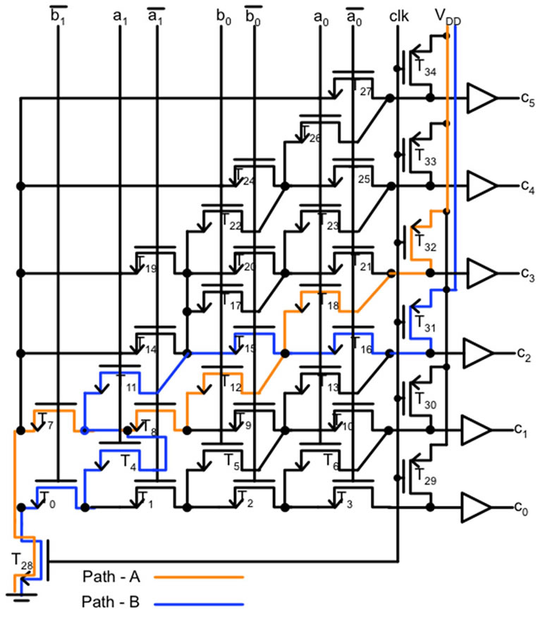
Figure 1. 2-b weighted BTC.
Typically, delay is identified based on the mean (μ) value from the delay distribution accounting only for intra-die variations. As inter-die variations are equally important, standard deviation (σ) from the delay distribution should be considered as well. The proposed circuit level optimization (CLO) algorithm ranks the critical paths based on the sum of mean and standard deviation (μ + σ), thus accounting for both intra-die and inter-die variations. In addition to critical path delay, CLO algorithm also minimizes delay sensitivity (τ = σ/μ) from process variations.
As charge/discharge time of transistors near vdd/ground is higher compared to the transistors near the output, high importance (weight) is assigned to transistors near vdd/ ground. As increasing size of transistor that appears in the most number of paths reduces the overall delay, the number of timing paths a transistor is present in is computed and denoted as repeats. The initial step in CLO algorithm is to size adjacent transistors on every path with a fixed size ratio of 1.1 for faster convergence. Once the repeat and the weight of all transistors are found, process-variation aware Monte Carlo simulations are performed to obtain delay profiles of each path. Then transistors on the top 20% critical paths are grouped to set-x, and their new sizes are increased and calculated by Equation (1).
As delay of critical path is dependent on loading from common channel-connected transistors, reducing loading reduces the overall delay. The 1st order connection transistors in the set-x are identified and grouped to set-y. Then, transistors in set-y that are not in set-x of the current iteration are grouped to set-z. For each transistor in set-z, it is checked if the transistor is present in set-x of previous iteration. If so, its size is decreased and calculated by Equations (2) and (3). If not, its size is decreased and calculated by Equation (4). Once new transistor sizes are determined, process-variation aware Monte Carlo simulations are performed to identify the new top 20% critical paths. If the new worst-case path delay is higher than in the previous iteration, sizes of transistors in set-z of the new worst-case path are changed to the average of new and old sizes. Iterations are repeated until the solution converges to an optimum.
 (1)
(1)
 (2)
(2)
 (3)
(3)
 (4)
(4)
3. Implementation of CLO Algorithm
Figure 1 shows a 2-b weighted binary-to-thermometricconverter (WBTC) used in parallel adders. At the onset of the CLO algorithm implementation, the critical path in 2-b WBTC is path-1 with a delay of 355 ps. After the first iteration, critical path delay reduced from 355 ps to 244 ps. Repeated iterations of the CLO algorithm reduced the delay to converge at an optimum of 157 ps while accounting for a 55.77% delay improvement. In addition, CLO algorithm also reduced delay uncertainty 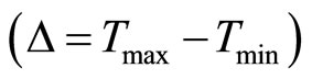 from 158 ps to 62 ps while accounting for 60.75% improvement as presented in Table 1.
Table 2 shows the percentage reduction in delay sensitivity (τ = σ/μ) of 2-b WBTC at different operating temperatures. With an average 9% reduction in delay sensitivity, the CLO algorithm works efficiently at different temperatures. This reduction in delay sensitivity of critical paths came at the cost of increase in delay sensitivity of non-critical paths (4, 5, 13, 14, 18, 28 and 31). Ranks from delays of these paths are shown in Table 3. Increase in delay sensitivity of these paths is acceptable as majorityof paths except path-31 are not critical paths. Efficiency of the CLO algorithm is further demonstrated through implementation on several circuits using IBM 130 nm CMOS process. The design profiles along with performance improvement are shown in Table 4, validating that CLO algorithm works effectively for circuits of various sizes and structures.
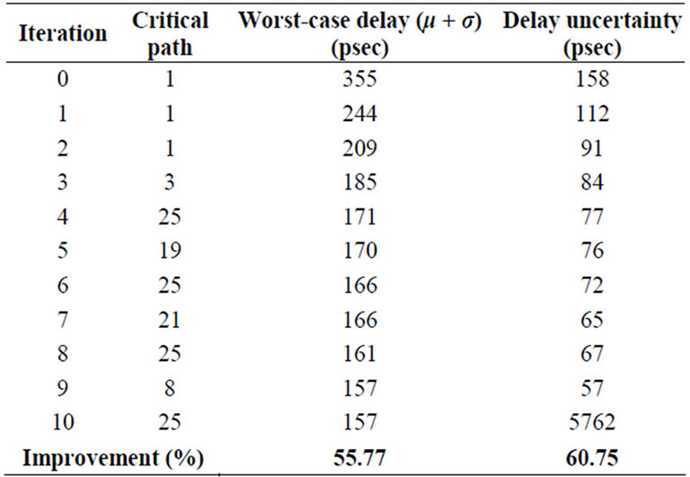
Table 1. 2-b WBTC delay convergence profile.
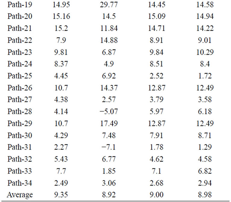
Table 2. 2-b WBTC delay sensitivity improvement (%) at different temperatures.
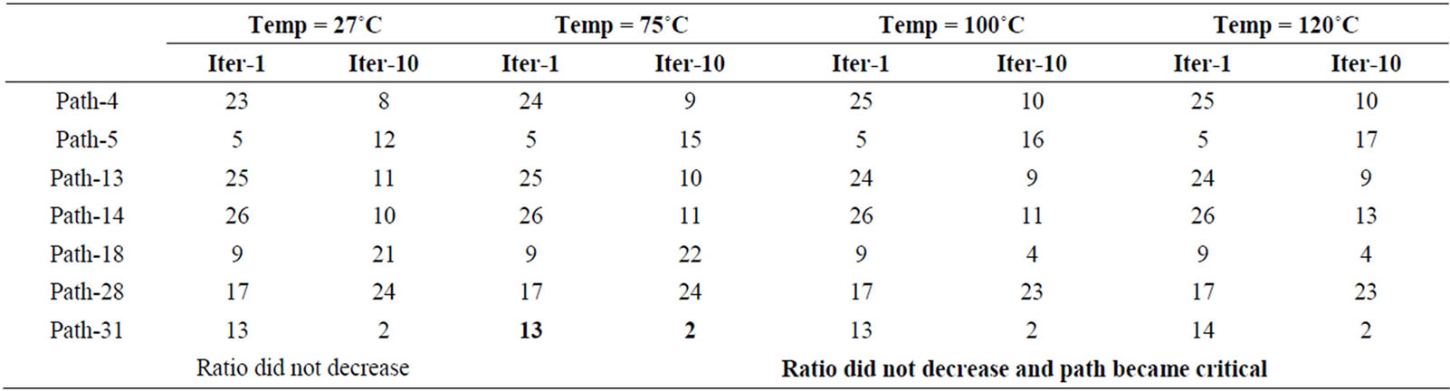
Table 3. 2-b WBTC path ranks at different iterations and temperatures.
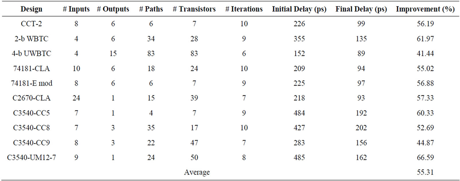
Table 4. Timing optimization results from CLO algorithm.
4. Design Level Optimization through Mixed-Static-Dynamic Circuits
Conventionally, synthesis tools perform design and optimization using static CMOS logic [13,14]. It is not uncommon for the synthesis tools to not find an acceptable solution in terms of timing. This challenge can be answered through utilizing the advantage of fast timing in dynamic logic. Dynamic logic has smaller gate capacitances compared to their static CMOS counterparts, which accounts for a significant speedup [3,15]. With static and dynamic logic having their respective advantages of low power and low delay, an optimal balance can be obtained by partitioning the design to use both static and dynamic logic in an effective manner.
At the architecture level, a common limitation in most design optimization flows is the limited accountability for process variations. Typically after placement and route, if a design fails to meet the timing constraints, optimization flow is re-iterated. Even after several iterations, design may still not meet the timing constraint, and miss the time-to-market window. The design level optimization (DLO) algorithm proposed in Figure 2 addresses some of these challenge in timing optimization, and also accounts for process variations. Utilizing the CLO algorithm proposed in previous section, the DLO algorithm partitions the design to effectively utilize both dynamic and static CMOS logic to meet the timing constraints.
The high level description of a design is input to a synthesis and optimization tool along with design constraints and target library. After synthesis and optimization, Static Timing Analysis (STA) is performed to identify the critical modules in the design. A strategy similar to the circuit level optimization algorithm is followed to find the critical modules in the design. These modules are identified based on the number (repeats) and length (weight) of critical paths in each. Once identified, custom dynamic CMOS circuits are designed at transistor level for greater flexibility, and timing optimization is performed using the circuit level optimization algorithm presented in the previous section.
Next, timing critical static CMOS modules from the commercial tool optimized design are replaced with black box models generated from the dynamic CMOS circuits. With the new design comprising both static and dynamic
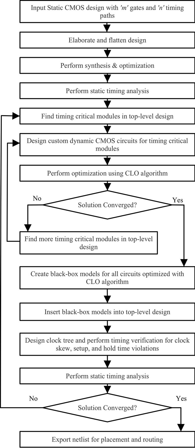
Figure 2. Design level optimization algorithm.
circuits, clock tree design and timing verification (clock skew, setup and hold time violation) is performed. If the timing constraints have been met, the design is exported for placement and routing. If not, the new timing critical modules are further identified and optimized using circuit level optimization algorithm presented in the previous section. This iterative process is a deterministic approach moving towards the optimum.
5. Implementation of DLO Algorithm
The design level optimization algorithm was implemented on a number of combinational circuits, including ISCAS benchmarks, and a high performance 64-b adder using IBM 130 nm CMOS process. Figure 3 shows the block diagram of the ISCAS benchmark c3540, an 8-b ALU with 1669 gates. After synthesis and optimization using the commercial tool, STA was performed. Delays of top 5 critical paths (highlighted) in c3540 were found to be 3.59 ns, 3.46 ns, 3.16 ns, 3.13 ns, and 2.97 ns respectively. Modules with highest delay in c3540 were found to be M5 with a delay of 1.63 ns, followed by M4 with a delay of 0.78 ns, and M12 with a delay of 0.63 ns (highlighted in Figure 3). The modules chosen for timing optimization from the STA are M5 and M12. Although M4 had the second highest delay, it was not chosen for optimization, as it does not repeat in as many critical paths as M5 and M12. This method of choosing only the critical modules during optimization is similar to circuit optimization algorithm, and helps limit the increase in area and power consumption.
Figure 4 shows the data flow schematic of M5-UM5_6 (critical module in M5). Though STA, modules CC5 and
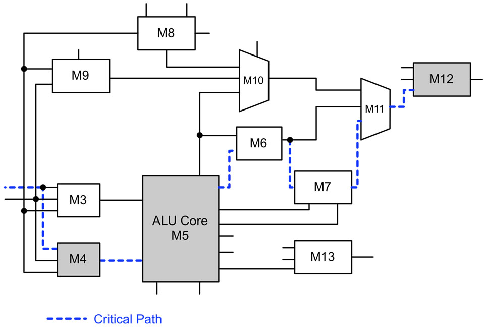
Figure 3. ISCAS benchmark-C3540 [16].
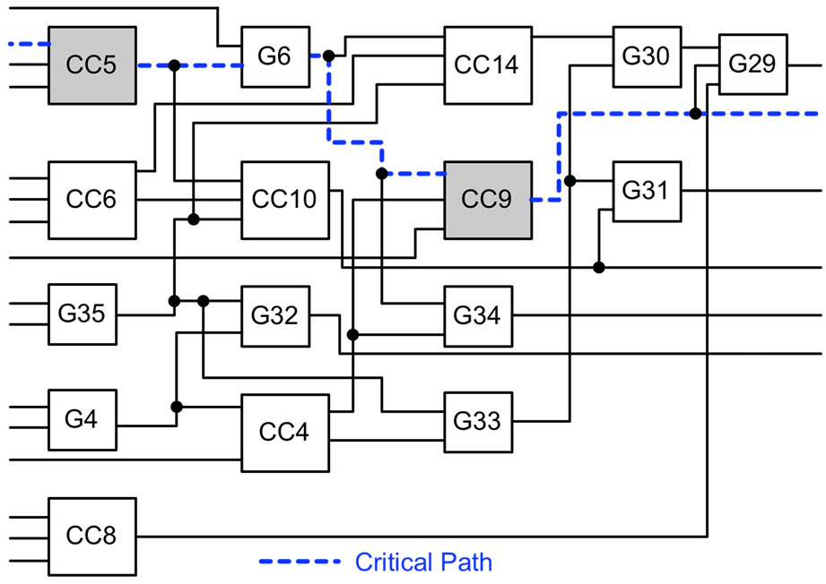
Figure 4. Timing critical modules in M5-UM5_6 of C3540.
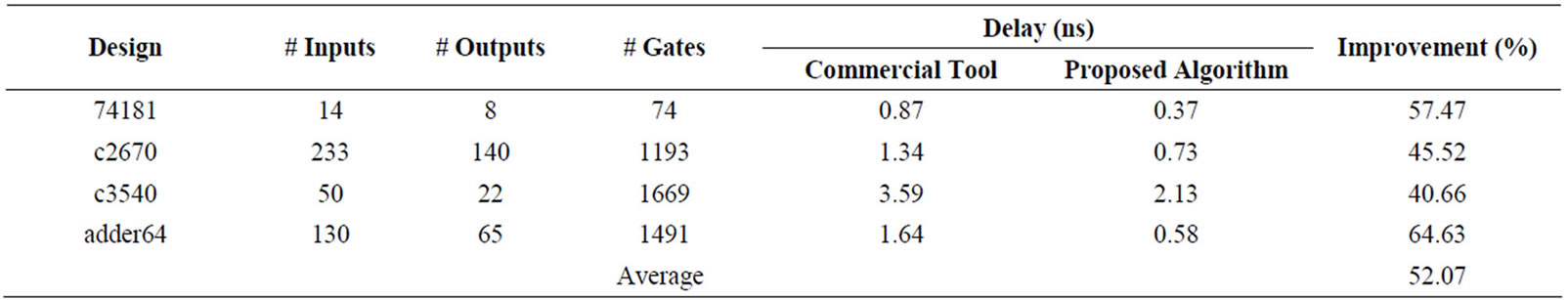
Table 5. Design level optimization algorithm results.
CC9 are found to be critical modules (highlighted in Figure 4), and are optimized using circuit level optimization algorithm. Accordingly, delays of these custom dynamic CMOS circuits were reduced by 57% and 39% respectively. Prior to implementing the circuit level optimization algorithm, CC5 had the highest delay in the first stage of M5-UM5_6. This optimization reduced delay of CC5, but made CC8 to be the module with highest delay in the first stage of M5-UM5_6. This is acceptable, as CC8 does not reside in the top 20% critical paths in C3540 so as not to limit the overall performance.
A similar approach was followed in optimizing M12-UM12_7 using the design level optimization algorithm, and its delay was reduced from 485 ps to 178 ps, a 63% improvement. One iteration of algorithm reduced delays of top five critical paths to 2.42 ns, 2.29 ns, 2.28 ns, 2.38 ns, 2.22 ns respectively. Through implementation of this optimization algorithm, the worst-case delay of c3540 was reduced from 3.59 ns to 2.13 ns, a 40% improvement over the results obtained from the commercially available state-of-the-art optimization tool. Similarly, the design level optimization algorithm was implemented on several other ISCAS benchmark circuits and a 64-b adder. Through implementation on c2670, the algorithm reduced the delay from 1.34 ns to 0.73 ns, a 45% improvement over the results obtained from acommercial tool. Also, the proposed algorithm reduced delay of 64-b adder from 1.64 ns to 0.58 ns. Timing optimization results obtained from the implementation of proposed design level optimization algorithm are shown in Table 5.
6. Conclusion
Effective performance optimization techniques are vital to the success of VLSI circuits as timing optimization and noise tolerance become ever-increasing problems with the relentless scaling of CMOS process technology. A desirable performance optimization technique should be able to improve the circuit robustness against all these challenges, be suitable for all logic functions, and have very low overhead in silicon area, delay, and power consumption. In this paper, such a performance optimization technique is proposed. First, we identify the complexity in timing optimization of dynamic CMOS logic circuits with high number of timing paths. Second, we propose a robust to process variation-aware load balance of multiple paths algorithm for timing optimization of dynamic CMOS logic. And last, we demonstrate the robustness of algorithm in optimization of delay, delay uncertainty, and delay sensitivity. Further, this paper also presented a design level optimization algorithm for mixed-static-dynamic CMOS logic, and has implemented it on several ISCAS benchmark circuits and a 64-b adder. Efficiency of the design level optimization algorithm flow is further validated through demonstrating an average worst-case delay improvement of 64% in comparison with state-ofthe-art commercial optimization tools.
REFERENCES
- J. Tschanz, K. Bowman and V. De, “Variation-Tolerant Circuits: Circuit Solutions and Techniques,” Design Automation Conference, San Diego, 13-17 June 2005, pp. 762-763.
- P. S. Zuchowski, P. A. Habitz, J. D. Hayes and J. H. Oppold, “Process and Environmental Variation Impacts on ASIC Timing,” IEEE/ACM International Conference on Computer Aided Design, San Jose, 7-11 November 2004, pp. 336-342.
- M. Zhao and S. S. Sapatnekar, “Timing-Driven Partitioning and Timing Optimization of Mixed Static-Domino Implementations,” IEEE Transactions on CAD of Integrated Circuits and Systems, Vol. 19, No. 11, 2000, pp. 1322-13360. doi:10.1109/43.892856
- J. P. Fishburn and A. E. Dunlop, “TILOS: A Posynomial Programming Approach to Transistor Sizing,” International Conference on Computer Aided Design, Delft, 7-10 October 1985, pp. 326-328.
- V. Sundararajan, S. S. Sapatnekar and K. K. Parhi, “Fast and Exact Transistor Sizing Based on Iterative Relaxation,” IEEE Transactions on CAD, Vol. 21, No. 5, 2002, pp. 568-581.
- A. R. Conn, I. M. Elfadel, W. W. Molzen Jr., P. R. O’Brien, P. N. Strenski, C. Visweswariah and C. B. Whan, “Gradient-Based Optimization of Custom Circuits Using a Static-Timing Formulation,” Design Automation Conference, New Orleans, 21-25 June 1999, pp. 452-459.
- K. A. Bowman, S. G. Duvall and J. D. Meindl, “Impact of Die-to-Die and Within-Die Parameter Fluctuations on the Maximum Clock Frequency Distribution for Gigascale Integration,” IEEE Journal of Solid-State Circuits, Vol. 37, No. 2, 2002, pp. 183-190. doi:10.1109/4.982424
- P. S. Zuchowski, P. A. Habitz, J. D. Hayes and J. H. Oppold, “Process and Environmental Variation Impacts on ASIC Timing,” IEEE/ACM International Conference on Computer Aided Design, San Jose, 7-11 November 2004, pp. 336-342.
- S. Borkar, T. Karnik, S. Narendra, J. Tschanz, A. Keshavarzi and V. De, “Parameter Variations and Impact on Circuits and Microarchitecture,” Design Automation Conference, Anaheim, 2-6 June 2003.
- C. H. Kim, K. Roy, S. Hsu, R. Krishnamurthy and S. Borkar, “A Process Variation Compensating Technique with an On-Die Leakage Current Sensor for Nanometer Scale Dynamic Circuits,” IEEE Transactions on VLSI Systems, Vol. 14, No. 6, 2006, pp. 646-649. doi:10.1109/TVLSI.2006.878226
- K. Yelamarthi and C.-I. H. Chen, “Process VariationAware Timing Optimization for Dynamic and MixedStatic-Dynamic CMOS Logic,” IEEE Transactions on Semiconductor Manufacturing, Vol. 22, No. 1, 2009, pp. 31-39. doi:10.1109/TSM.2008.2011665
- V. Chandrasekhar, C.-I. H. Chen and K. Yelamarthi, “LowCost Low-Power Self-Test Design and Verification for On-Chip ADC in System-On-a-Chip Applications,” IEEE Instrumentation and Measurement Technology Conference, Sorrento, 24-27 April 2006.
- Synopsys Design Compiler, http://www.synopsys.com
- Cadence Encounter, http://www.cadence.com
- R. Puri, “Design Issues in Mixed Static-Dynamic Circuit Implementation,” Proceedings of International Conference on Computer Design, San Jose, 5-7 October 1998, pp. 270-275.
- M. Hansen, H. Yalcin and J. P. Hayes, “Unveiling the ISCAS-85 Benchmarks: A Case Study in Reverse Engineering,” IEEE Design and Test, Vol. 16, No. 3, 1999, pp. 72-80. doi:10.1109/54.785838