Journal of Modern Physics
Vol.2 No.9(2011), Article ID:7140,5 pages DOI:10.4236/jmp.2011.29119
Optoelectronic Characterization of Chemical Bath Deposited CdxCo1−xS Thin Film
1Department of Physics, University of Port Harcourt, Port Harcourt, Nigeria
2Department of Industrial Physics, Ebonyi State University, Abakaliki, Nigeria
E-mail: *panaceamee@yahoo.com
Received February 1, 2011; revised May 20, 2011; accepted May 30, 2011
Keywords: CdxCo1−xS, CVD, Thin Films, Band Gap, Vegard’s Law
ABSTRACT
Cadmium Cobalt Sulphide (CdxCo1−xS) thin film was deposited on microscopic glass substrate using chemical bath deposition technique at room temperature from aqueous solutions of Cadmium Chloride, Cobalt Chloride and Thiourea in which ammonium solution was used as complexing agents. The optical properties were characterized using the absorbance and transmission measurement from Unico UV-2102 PC spectrophotometer, at normal incidence of light in the wavelength range of 200 - 1000 nm. We report the deposition and optimization of the growth parameter with respect to time which showed that the band gap energy and the composition verified from the extended Vegard’s law are highly dependent on deposition time. The average transmittance of the film in VIS-NIR region ranges between 30% and 78% with absorbance range of 0.15 - 0.47 within the same wavelength range. The film was also observed to exhibit poor reflectance (11 < R% < 20) which declined albeit exponential within the entire studied wavelength range. From absorbance and transmittance spectra, the band gap energy determined for the film deposited at various time: 19 h, 21 h and 24 h are 2.25 eV, 2.17 eV and 2.05 eV respectively, in that order. The composition of the ternary system for 19 h; 21 h, and 24 h were found to be (x = 0.75; 0.83 and 0.94), respectively. Other optical and dielectric properties of the films were also characterized. Based on the exhibited properties of the film, it can be concluded that it is a promising material for selective coatings for solar cells; effective coatings for poultry houses; use as antireflective coating materials, and for fabrication of optoelectronic devices.
1. Introduction
The derivatives of CdS to ternary chalcogenide materials in recent time have witnessed a lot of research interest possibly for their applications in the field of optoelectronic devices. CdxCo1−xS is one of the ternary derivatives which have been studied as a good candidate for wide band gap material for photovoltaic and photoconducting devices. Its band gap can be harnessed from 2.37 - 2.43 eV (CdS) to 3.20 eV (CoS). The addition of Co to CdS enhances the open-circuit current in the heterojunction devices generally due to decrease in the window absorption losses [1].
Various deposition techniques such as spray pyrolysis [2], metal organic chemical vapour deposition (MOCVD) [3], and chemical bath deposition (CBD) [4] have been used to deposit Cadmium cobalt sulphide. However, the popularization of the chemical bath deposition (CBD) technique in recent decades for thin film deposition no doubt is due to its relatively low cost and simple method for the deposition of high quality and large area films [5-7], wider choice of materials to be used [4], and facilitates better orientation of crystallites with improved grain structure [5].
The CBD is an ion-ion exchange which involves slow release of S2– and controlled free Cd2+ and Co2+ ions in an alkaline solution. In this work, thiourea 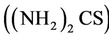 is used as the sulphiding agent. To control the hydrolysis of the metal ion and impart some stability to the bath which, normally will hydrolyze, and precipitate, a chelating agent is used. The deposition of CdS in the bath is simple but the introduction of Co complicates the entire deposition process since the solubility product of CdS (
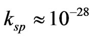 ) [8,9] and CoS (
 ) [9,10] differ by several orders of magnitude with varying stability constant of the Cd and Co precursors. To avoid these difficulties, most researchers have opted for the use of acidic bath deposition [8] and multilayer processing [11]. However, it has been argued that if CdS can successfully be deposited from similar bath, then the possibility of depositing the true ternary compound could be enhanced as the difficulty of the gross insolubility of Co hydroxyl species would be minimized at low pH.
In this work, we report the deposition of CdxCo1−xS and the characterization of the various optical and dielectric properties with the time of deposition as a controlling parameter. The composition of the ternary film is also calculated using the extended Vegard’s law.
2. Experimental Procedure
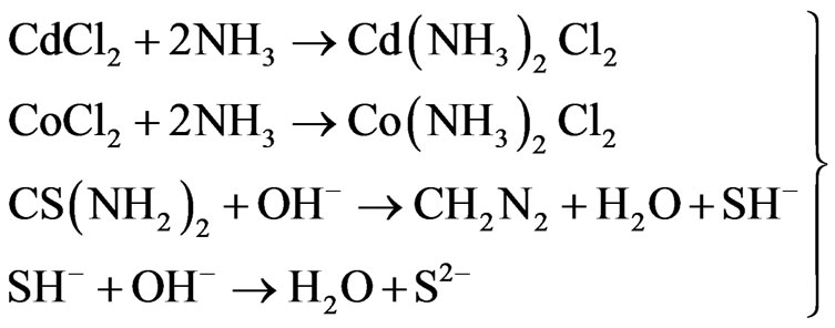
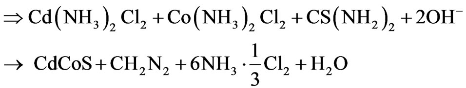
The Cadmium Cobalt Sulphide (CdxCo1−xS) thin film was deposited on glass slides using the Chemical Bath Deposition (CBD) technique at room temperature (300 K). The micro substrates were initially degreased in HCl for 24 h, cleaned in cold water with detergent, rinsed in distilled water and then dried in open air. The reaction bath for the deposition of CdxCo1−xS contained 1.0 M 2 mL CdCl2; 0.25 M 3 mL CoCl2; 1.0 M 10 mL thiourea; 14.0 M 5 mL NH3 and 35 mL of distilled water which were carefully added in that order. The substrates were allowed in the reaction bath for 19, 21 and 24 h, respectively. The mixtures were carefully stirred to maintain homogeneity and constant pH which was close to 6.5. The kinematics of the reaction of the complex ion formation and subsequent film deposition process are:
 (1)
(1)
 (2)
(2)
From the kinematics of the film deposition, it can be seen that the sulphide ions are released from the hydrolysis of thiourea ( ) while the Co2+ and Cd2+ ions formed complexes: Cobalt diamine chloride (
 ) and Cadmium diamine chloride (
 ), respectively by reacting with NH3. These two complexes adhered firmly to the substrate surface forming a heterogeneous nucleation and subsequently, growth by ionic exchange of S2- ions. The “as-deposited” CdxCo1−xS thin film is yellow in colour and specularly reflective, transparent, homogeneous and adhered firmly to the glass slide. The normal incidence transmittance and absorbance spectrum of the deposited films were characterized using UNICO UV-2102 PC spectrophotometer in the UV-VIS-NIR region and the solid state and optical properties calculated. The measurements were taken under the parametric conditions of normal incident, ambient temperature and uncoated microscopic glass slide as reference. The optical properties investigated were Absorbance (A); Transmittance (T) and Reflectance (R) which were subsequently used to calculate other properties: Extinction coefficient (k); Refractive index (n); Dielectric constant (
 ); Optical conductivity (σ) and the band gap energy (Eg) which were deduced from their various relations already well established in literature [12,13].
3. Results and Analysis
Figures 1-9 and Table 1 show the various (optical and dielectric) properties of the CdxCo1−xS thin film being studied.
3.1. Optical and Dielectric Properties
The plots of the absorption coefficient against photon energy are as shown in Figure 1. These absorption spectra which is the most direct and possibly the easiest method for probing the band structure of semiconductors are employed in the determination of the band gap energy Eg.
The variation of the spectra transmittance (T%) and reflectance (R%) with the photon wavelength are as shown in Figures 2 and 3 respectively. The film show high transmittance in the ultraviolet, visible, and infra
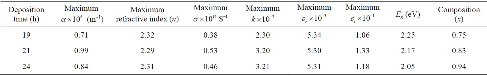
Table 1. Compositional; optical and dielectric and properties of CdxCo1−xS thin films.
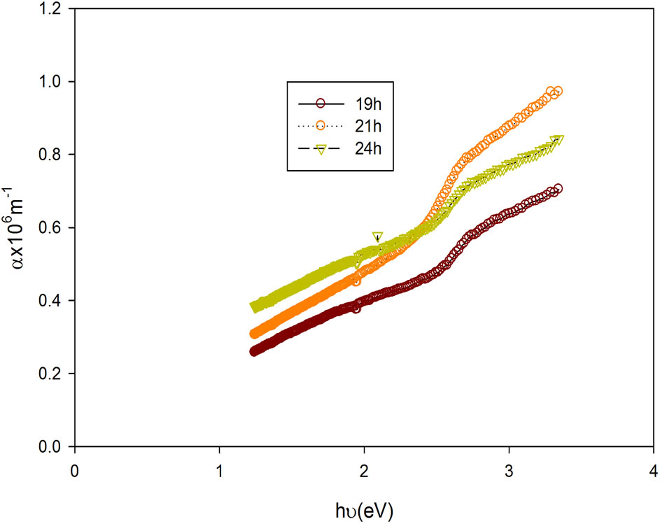
Figure 1. Absorption coefficient as a function of photon energy (hν) for CdxCo1−xS thin film.

Figure 2. Transmittance (T) as a function of wavelength (λ) for CdxCo1−xS thin film.
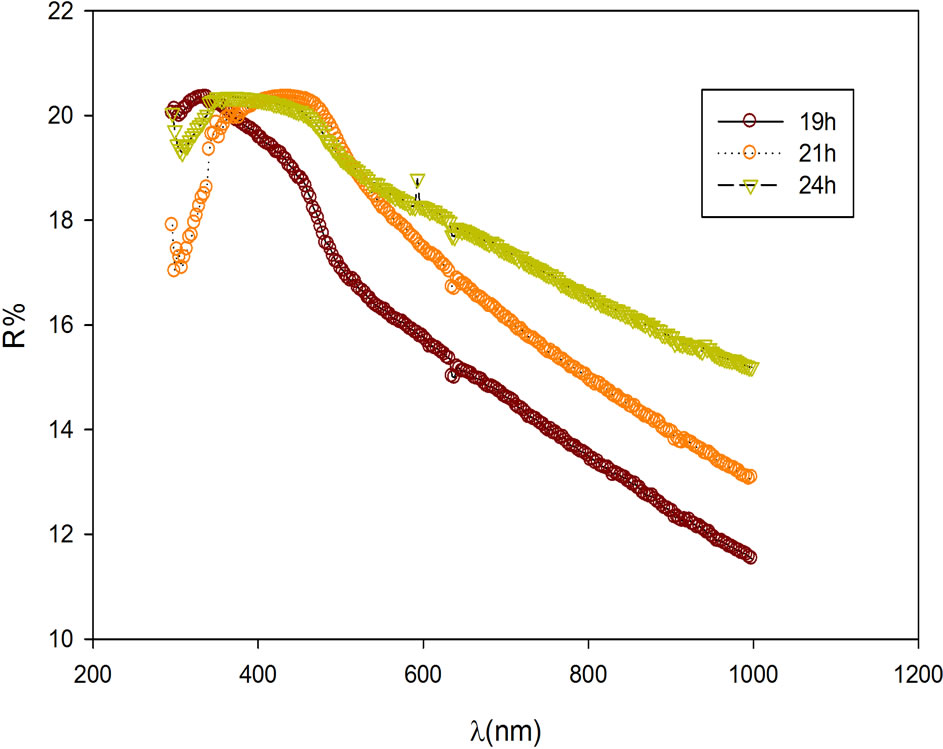
Figure 3. Reflectance (R) as a function of wavelength (λ) for CdxCo1−xS thin film.

Figure 4. Refractive index (n) as a function of photon energy (hν) for CdxCo1−xS thin film.
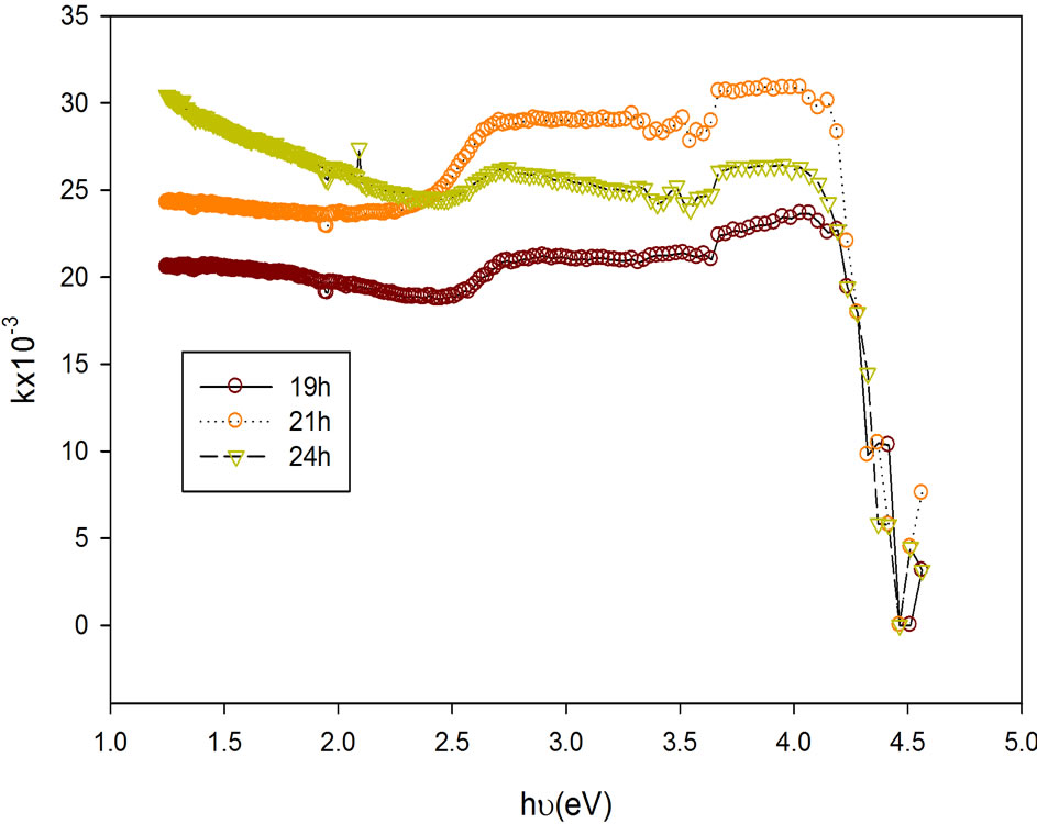
Figure 5. Extinction coefficient (k) as a function of photon energy (hν) for CdxCo1−xS thin film.
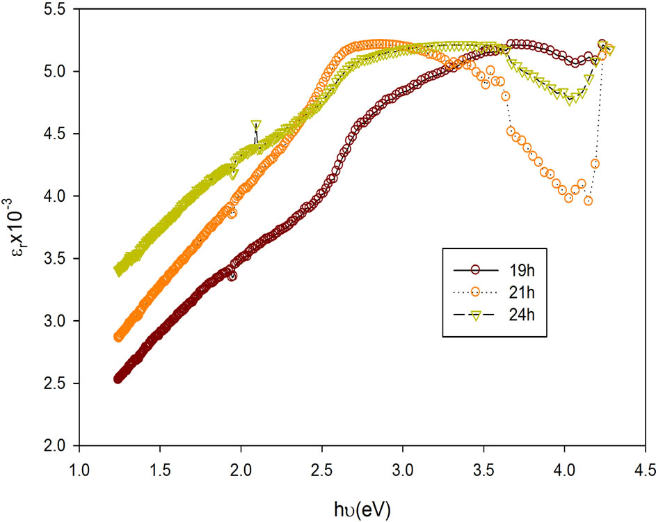
Figure 6. Real dielectric constant as a function of photon energy (hν) for CdxCo1−xS thin film.

Figure 7. Imaginary dielectric constant as a function of photon energy (hν) for CdxCo1−xS thin film.

Figure 8. Plots of conductivity (σ) as a function of photon energy (hν) for CdxCo1−xS thin film.
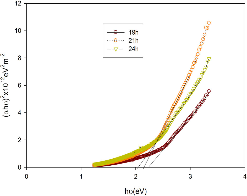
Figure 9. Plots of (αhν)2 as a function of photon energy (hν) for CdxCo1−xS thin film.
red regions of the electromagnetic spectrum. Conversely, the reflectance of the film is found to be low (6% - 20%) within the same region. These high transmittance and low reflectance make the film good materials for antireflection coatings and for solar thermal applications in flat-plate collectors and house heating for solar chick brooding.
Figure 4 relates refractive index (n) against photon energy and Figure 5 shows the plot of the extinction coefficient (k) of the film samples to the photon energy. The range of the refractive index is 1.6 - 2.3 with peak value at photon energy of 3.21 eV while the extinction coefficient had minimum values at photon energy of 2.55 eV for all the films but different minimum values (see Table 1).
The variations of the dielectric constant (real and imaginary) are as shown in Figures 6 and 7. Figure 8 is the plot of the optical conductivity with the photon energy. It can be inferred that the film has maximum values in the range 0.35 – 0.52 × 10¹⁴ S–1 and minimum values between 0.09 – 0.16 × 10¹⁴ S–1.
The plot of (αhν)2 as a function of photon energy (hν) for the film is as shown in Figure 9. It can be observed that the deposition time significantly affected the band gap energy. For the film deposited for 19 h, it is 2.25 eV; film deposited for 21 h, it is 2.17 eV and that deposited for 24 h is 2.05 eV. It can generally be inferred that as the deposition time gradually increased, the band gap energy declined. This observed decrease in Eg may be attributed to attainment of stability of the metal ions in the bath.
3.2. Compositional Analysis
Applying the modified virtual crystal approach proposed by Phillips [13], we note that Shimakawa has accounted for compositional variations in a ternary system [14,15]. To achieve this, we will follow the approach proposed by Yen-Kuang et al. [16] where they argued that the highly compositional dependent bowing parameter obeys a thirdorder polynomial [17] and expand the non-linearity effect introduced into the Vegard’s relation in power series as:
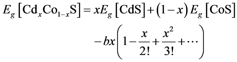 (3)
(3)
where b is the bowing parameter. We used b = 0.7 eV [16] to calculate the value of x for the films deposited at various deposition time as:
19 h: 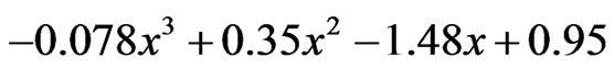 which gives x as 0.75.
21 h:  which gives x as 0.83.
24 h: 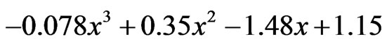 which gives x as 0.94.
Thus, we calculate the composition of the ternary CdxCo1−xS thin film as Cd0.75Co0.25S; Cd0.83Co0.17S and Cd0.94Co0.06S, respectively for the various deposition times 19 h; 21 h, and 24 h in that order. The important remark that can be made from this is that time of deposition affects the composition of the ternary system.
4. Conclusions
The optical and dielectric properties induced by varying the deposition time of CdxCo1−xS has been investigated. The energy band gap was found to decrease with the deposition time and this was used to evaluate the composition of the ternary system. The calculated band gap energy is observed to lie between the band gap of CdS (2.37 - 2.43 eV) and CoS (2.95 - 3.20 eV) which, is close to energy gap of CdS. This shows that the film is rich in cadmium. Most significantly, it can be observed that the cobalt was like an impurity atom in the CdCoS system and it’s percentage decreased significantly with increasing annealing temperature. The properties of the film characterized clearly positions this material as a possible candidate for fabricating optoelectronic devices, antireflective coatings etc.
REFERENCES
- T. Yamaguchi, Y. Yamamoto, T. Tanaka, Y. Demizu and A. Yoshida, “(Cd,Zn)S Thin Films Prepared by Chemical Bath Deposition for Photovoltaic Devices,” Thin Solid Films, Vol. 281-282, 1996, pp. 375-378.
- E. Bacaksiz, M. Tomakin, M. Attunbas, M. Parlac and T. Colakoglu, “Structural, Optical and Magnetic Properties of Cd1−xCoxS Thin Films Prepared by Spray Pyrolysis,” Physica B: Condensed Matter, Vol. 403, No. 19-20, 2008, pp. 3740-3745. doi:10.1016/j.physb.2008.07.006
- T. L. Chu, S. S. Chu, J. Britt, C. Ferrikide and O. Q. Wu, “Cadmium Zinc Sulfide Films and Heterojunctions,” Journal of Applied Physics, Vol. 70, No. 5, 1991, pp. 2688-2693. doi:10.1063/1.349384
- F. I. Ezema, “Optical Characterization of Chemical Bath Deposited Bismuth Oxyiodide (BiOI) Thin Films,” Turkish Journal of Physics, Vol. 29, No. 2, 2005, pp. 105-114.
- R. S. Mane and C. D. lokhande, “Chemical Deposition Method for Metal Chalcogenide Thin Films,” Material Chemistry and Physics, Vol. 65, No. 1, 2002, pp. 1-31. doi:10.1016/S0254-0584(00)00217-0
- R. Poulomi, and S. Kumar, “Chemical Bath Deposition of MoS2 Thin Film Using Ammonium Tetrathiomolybdate as a Single Source for Molybdenum and Sulphur,” Thin Solid Films, Vol. 496, No. 2, 2006, pp. 293-298. doi:10.1016/j.tsf.2005.08.368
- C. A. Estrada, P. K. Nair, M. T. S. Nair, R. A. Zingaro and E. A. Meyers, “Chemical Bath Deposition of ZnSe and CuSe Thin Films Using N,N-Dimethylselenourea,” Journal of Electrochemical Society, Vol. 141, No. 3, 1994, pp. 802-806. doi:10.1149/1.2054814
- D. S. Boyle, O. Robbe, D. P. Halliday, M. R. Heinreich, A. Bayer, O. Brien, P. D. J. Otway and M. D. G. Potter, “A Novel Method for the Synthesis of the Ternarythin Film Semiconductor Cadmium Zinc Sulfide from Acidic Chemical Baths,” Journal of Materials Chemistry, Vol. 10, 2000, pp. 2439-2441. doi:10.1039/b005544l
- G. Hodes, “Chemical Solution Deposition of Semiconductor Films,” CRC Press, New York, 2000.
- J. Zhou, X. Wu, GTeeter, B. To, Y. Yan, R. G. Dhere and T. A. Gessert, “CBD-Cd1−xZnxS Thin Films and Their Application in CdTe Solar Cells,” Physica Status Solidi, Vol. 241, No. 3, 2004, pp. 775-778. doi:10.1002/pssb.200304218
- I. O. Oladeji, L. Chow, C. Ferekides, V. Viswanathan and Z. Zhao, “Metal/CdTe/CdS/Cd1−xZnxS/TCO/Glass: A New CdTe Thin Film Solar Cell Structure,” Solar Energy Materials & Solar Cells, Vol. 61, No. 2, 2000, pp. 203-211. doi:10.1016/S0927-0248(99)00114-2
- J. Singh, “Optical Properties of Condensed Matter and Applications,” John Wiley & Sons, Hoboken, 2006.
- K. Shimakawa, “On the Compositional Dependence of the Optical Gap in Amorphous Semiconducting Alloys,” Journal of Non-Crystalline Solids, Vol. 43, 1981, pp. 229-244. doi:10.1016/0022-3093(81)90119-8
- J. C. Phillips, “Bond and Band in Semiconductors,” Academic Press, New York, 1973.
- K. Osamura, S. Naka and Y Murakami, “Preparation and Optical Properties of Ga1−xInxN Thin Films,” Journal of Applied Physics, Vol. 46, 1975, p. 3432-3438. doi:10.1063/1.322064
- K. Yen-Kuang, C. Han-Yi, Y. Sheng-Horng, L. Bo-Ting and C. Mei-Ling, “Bowing Parameter of Zincblende InxGa1−xN,” Optics Communication, Vol. 280, No. 1, 2007, pp. 153-156. doi:10.1016/j.optcom.2007.07.058
- M. C. Tamargo, “Optical Properties of Electronic Structure of Semiconductors,” In: C. Hernandez, Ed., II – VI Semiconductor Materials and Their Application, Taylor and Francis, New York, 2002, pp. 113-170.