World Journal of Nano Science and Engineering
Vol.05 No.04(2015), Article ID:62489,6 pages
10.4236/wjnse.2015.54022
Method of Formation of Waveguides on the Basis of Any Polymeric Materials
Valentin Tsvetkov1*, Sergei Pasechnik1, Aleksei Dronov2, Jacob Y. L. Ho3, Vladimir Chigrinov3, Hoi-Sei Kwok3
1Problem Laboratory of Molecular Acoustics, Moscow State University of Instrument Engineering and Computer Sciences, Moscow, Russia
2National Research University of Electronic Technology, Moscow, Zelenograd, Russia
3State Key Laboratory on Advanced Displays and Optoelectronics Technologies, Clear Water Bay, Kowloon, Hong Kong, China

Copyright © 2015 by authors and Scientific Research Publishing Inc.
This work is licensed under the Creative Commons Attribution International License (CC BY).
http://creativecommons.org/licenses/by/4.0/


Received 24 November 2015; accepted 28 December 2015; published 31 December 2015
ABSTRACT
This paper describes a new type of polymeric waveguides which has the core, cladding medium and active nodes made from the same material. Part of the polymer is removed in cladding medium by formation of nanopores. The pores can be filled with liquid crystals (LC) in order to create an active composite medium needed for electrically controlled nodes formation.
Keywords:
Polymeric Materials, Nanopores, Waveguides, Optical

1. Introduction
Recently, a large number of works was devoted to polymeric materials applicable for optoelectronic waveguide devices, including waveguide films formation technology descriptions and their optical characteristics.
The polymers show some advantages over commonly used crystalline materials such as Si, Ge or multicomponent semiconducting compounds. In particular, they provide a simple and relatively cheap technology applicable for production of big size units. For example, thin polymers films are well suited for formation of the plane waveguides of micrometer thickness [1] -[5] . In most cases, the polymer waveguides are formed by trivial methods extrusion, or by spin-coating process [4] . It is necessary in these cases to provide the lower value of a refractive index (RI) in the cladding part of a waveguide with the value of the RI in the central part (the core of a waveguide). Usually, this aim is achieved by formation of outer (cladding) layers of a waveguide from materials such as polymethyl methacrylate (PMMA), or perfluorinated polyimide (PFPI) with relatively low values of the RI. Such decision creates additional technological difficulties. In particular, input and output parts of the waveguides with the active nodes have an optical and structural coupling problem.
2. Materials and Methods
To avoid these difficulties, it is desirable to use the same material for both the core and cladding waveguide parts. Moreover, in this case it is possible to obtain controlled cladding layer by using an electrically controllable materials, such as a LC’s. It can be applied for elaboration and production of new waveguide units such as X, Y splitters, deflectors, wavelength selectors, etc. In this paper we describe a new method of waveguide formation based on usage of the same polymer for both core and cladding parts. It is realized by formation in the cladding part of the waveguide the system of opened or closed pores, which provide a reduction of the RI in cladding part. The degree of the reduction depends on both the pore size and pore density. The filling of pores with liquid crystals may provide changes of effective refractive index of a cladding via electric field, which makes possible to obtain the electrically controlled waveguide. Earlier we used similar polyethylene terephthalate films (PET) as the working medium for the displays [6] [7] .
3. Experiments and Explanations
To verify the proposed method, we used a membrane series made by Institute of Nuclear Research in Dubna (Russia). Membrane thickness was 12 and 23 micrometers. The series included more than 20 membranes with pore diameters from 20 nanometers to 5 micrometers with different pore densities.
PET films were made by extrusion and therefore have significant optical anisotropy [8] . The published data and the results of our measurements show that the mentioned above materials have high losses of light of order of 7.3 dB/cm for λ = 0.473 μ; 4.0 dB/cm for λ = 0.633 μ and 1.44 dB/cm for λ = 1.550 μ.
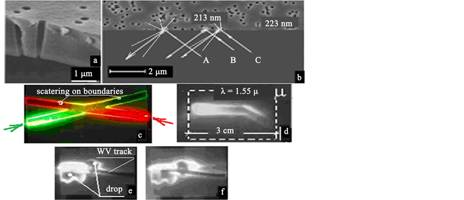
The images shown in Figures 1(c)-(f) demonstrate that the light passes along the waveguide center (the waveguide core) surrounded by cladding medium permeated by the pores.
We have found that there is significant light scattering in the region of interface between porous and non- porous parts of the film at the pore’s diameters comparable or even smaller than a wavelength of propagating light beam (see bright waveguide core framing). This effect was observed in the whole range of wavelength (450,∙∙∙,1550 nm) used in experiments. It can be explained as an integral effect of scattering from a number of chaotically distributed cylindrical obstacles. Different aspects of light scattering from individual cylinders im-
Figure 1. Cross-section of the PET film with pores (a); explanation of light beam reflectance from the interface of a pore less film and a film having randomly arranged pores (b); (c) (d) light wave propagation in some waveguide elements; (e) (f) wave tracks passing the drops.
mersed in isotropic media were considered previously [8] - [10] . In our case, polymer film can be anisotropic which prevent the direct application of previously obtained results. Moreover, usage of liquid crystals as anisotropic media inside anisotropic film made theoretical description of the problem to be quite complicated. So, we focus firstly on the qualitative explanation of the obtained results.
We believe that the observed scattering effect appears due to the pores random distribution in cladding part, resulting in a section between the core and the waveguide cladding medium looks like a “matte surface” (Figure 1(b)). To prove this, a drop of an isotropic liquid with a refractive index greater than the film’s refractive index was placed at the interface. It resulted in evolution of the scattering region due to penetration of a liquid into pores, as shown in Figure 1(e) and Figure 1(f). In particular, it can be seen that diffuse scattering disappears as the droplet spreads.
A similar scattering disappearance effect can be obtained by filling pores with LC and further application of a control voltage, which makes possible to form an electrically controlled node.
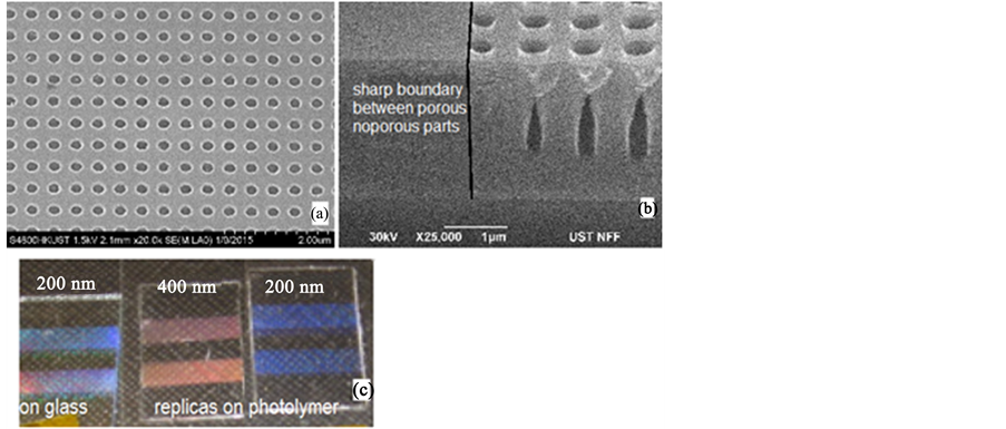
We believe that one of the ways to eliminate the parasitic scattering at the boundaries is the usage of regular or quasi-regular pore matrices formation. To check this thought, the membranes with a strictly regular arrangement of pores were produced (Figure 2).
For the first experiments, the polyimide films of 4 micrometer in thickness with the RI = 1.8 were used. Films were formed by spin coating the glass substrates of sizes 2 × 2 cm. The non-through pores of 2 μm in depth with the pores’ diameter equal to 200 or 400 nm were obtained by interference lithography and ion-plasma etching methods. The distance between the pores was equal to 400 or 800 nm, respectively (Figure 2). In addition, to enhance the future technological production of waveguides, the successful attempt to transfer by replication the pores film topography from the glass substrate to the polymer substrate was made. Figure 2(c) shows that replica has the same spectral composition as the original sample.
The obtained difference between RIs of porous and non-porous parts (about 0.35) allows, in principle, to support a waveguide regime of propagating electromagnetic waves in wide wavelength range (from UV to THz).
Consequently, according to the proposed technology it is possible to use any other polymer film with different RI. It extends the possibility of application of different types of polymer, like TOPAS, widely used for production of THz waveguides [11] .
Since both the pore’s diameter and period of a pore distribution are smaller than the visible light wavelengths, a formation of the super-wave grating (SWG) regime is possible, which leads to a noticeable bright staining. This phenomenon can be used to build color displays without any polarizers or dyes, if switching on and off modes of the grating will be realized , for example, by filling the pores with electrically active medium, such as the LC’s and application of a control voltage.
Figure 2. (a) Samples of waveguides structures: a-distribution of pores; (b) cross section of the sample; (c) views of WG deposited on glass substrate and its replicas on photopolymer.
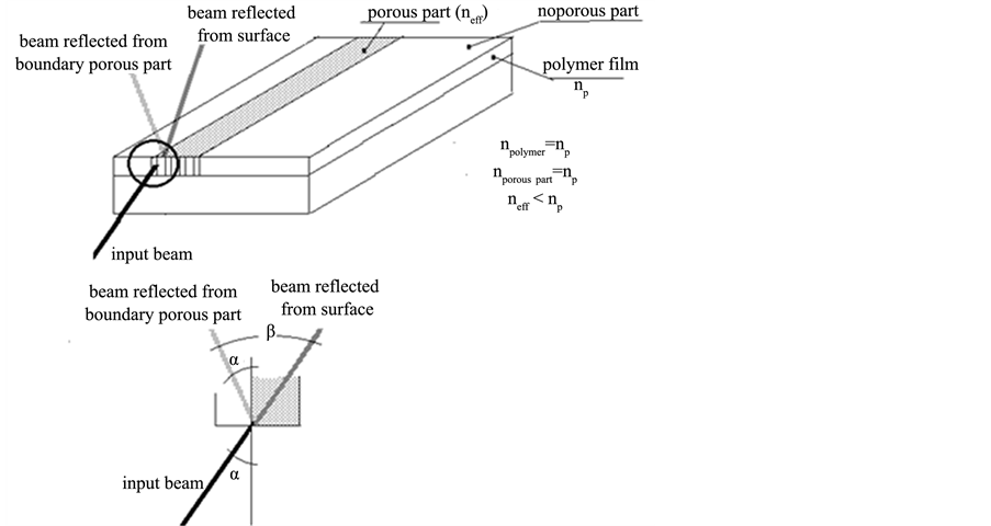
At illumination of the edge of a substrate by a non-collimated laser beam of a diameter 3 - 4 mm, the input beam was partly reflected from the outer surface of the substrate and partly transmitted to the waveguide. The transmitted beam crossed the boundary between the porous and non-porous parts (Figure 3) at some small angle.
Afterwards, this beam was partly reflected from the interface in the accordance with geometrical optics laws, namely:
1. The angles of incidence and reflection are equal.
2. The reflected light is mainly polarized in the direction perpendicular to the waveguide plane. The boundary between the two parts of the waveguide shows no sign of scattering, contrary to the case of inherent scattering at the boundaries of the waveguide observed at a random arrangement of pores.
We observed, that the reflected beam could be totally deleted by placing onto waveguide surface a drop of an isotropic liquid with the RI equal to or greater than the polymer film RI. In this case the introduced beam was not reflected from the interface between the porous and nonporous regions of the film and penetrated into the porous part filled with a liquid, due to matching of the RIs. At the same time, the reflection occurred at the boundary between regions with filled and empty pores.
Obviously, that a similar effect can be induced by application of electric field to the pores filled with the LC's. Thus the active element can be created from the same polymer as the waveguide core.
The above described experiments confirm a possibility to control light beams propagating in the waveguide.
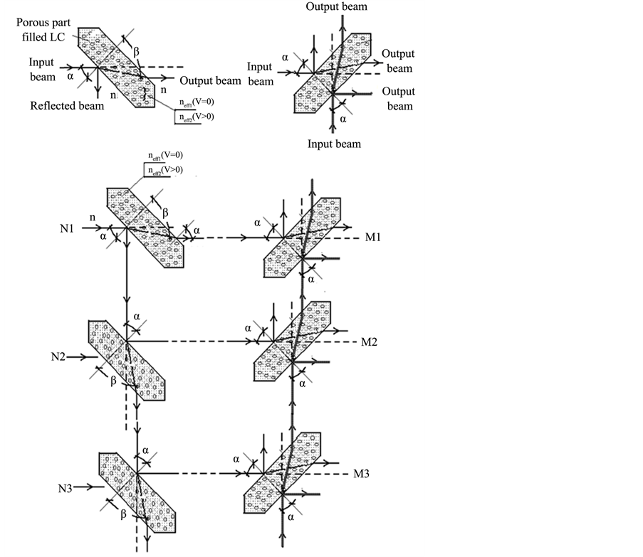
It makes possible to get electrically control boundary, which can be switched between modes “light reflects” and “light passes”. With the set of such interfaces, it is possible to build a multi-step M × N channel router similar to that shown in Figure 4.
4. Conclusions
1. It was shown experimentally that usage of the proposed technology provided a production of any passive waveguide structure from any available polymer. The perspective of an electric control of light beams propagating in waveguides, when the pores will be filled in with electrically controlled material, such as LC, is considered. Light losses in such waveguides are determined only by their own material loss, because any manipulations will not have effect on core properties.
2. The proposed methods and technologies are universal and allow to create waveguide structures for different wavelengths because the difference of the core and cladding medium refractive indices is high (0.35), and unattainable by any other waveguide formation method. An important consequence of such difference is the ability
Figure 3. Path of the rays in the reflection from the interface.
Figure 4. Router M × N canals.
to handle any wavelengths radiation from UV to THz.
Now the work is in the stage of progress.
Conflict of Interests
The authors declare that there is no conflict interests regarding the publication this paper.
Acknowledgements
This work was partially supported by the Ministry of Education and Science of the Russian Federation (Grant No. 3.1921.2014/K) and by the City University of Hong Kong under Grants SRG 7002475 and SRG 7002866.
Cite this paper
ValentinTsvetkov,SergeiPasechnik,AlekseiDronov,Jacob Y. L.Ho,VladimirChigrinov,Hoi-SeiKwok, (2015) Method of Formation of Waveguides on the Basis of Any Polymeric Materials. World Journal of Nano Science and Engineering,05,213-218. doi: 10.4236/wjnse.2015.54022
References
- 1. Uddin, M.A. and Chan, H.P. (2008) Materials and Process Optimization in the Reliable Fabrication of Polymer Photonic Devices. Journal of Optoelectronics and Advanced Materials, 10, 1-15.
- 2. Zhou, S.F., Reekie, L., Chan, H.P., Chow, Y.T., Chung, P.S. and Luk, K.M. (2010) Polymer Fiber Bragg Gratings for the THz Region. Optics Express, 8, 11707-11712.
- 3. Low, A.L.Y., Singh, G.K., and Yong, Y.S. (2004) High-Index and Low Loss Polyethylene Terephthalate Optical Waveguides. Optical and Quantum Electronics, 36, 997-1003.
http://dx.doi.org/10.1007/s11082-004-2039-2 - 4. Iiyama, K., Ishida, T., Ono, Y., Maruyama, T. and Yamagishi, T. (2011) Fabrication and Characterization of Amorphous Polyethylene Terephthalate Optical Waveguides. IEEE Photonics Technology Letters, 23, 275-277.
- 5. Iiyama, K., Ishida, T., Sasaki, K., Kitamura, K. and Maruyama, T. (2011) Low Loss Amorphous Polyethylene Terephthalate (PET) Optical Waveguides. 16th Opto-Electronics and Communications Conference, OECC 2011, Taiwan, 4-7 July 2011, 301-302.
- 6. Semerenko, D., Shmeliova, D., Pasechnik, D., Murauskii, A., Tsvetkov, V. and Chigrinov, V. (2010) Optically Controlled Transmission of Porous Polyethylene Terephthalate Films Filled with Nematic Liquid Crystal. Optics Letters, 35, 2155-2157.
http://dx.doi.org/10.1364/OL.35.002155 - 7. Semerenko, D., Shmeliova, D., Pasechnik, S., Chigrinov, V., Murauskii, A. and Tsvetkov, V. (2010) The Investigation of Polarization Properties of the Porous PET Films Filled with LC. International Conference on Advanced Infocomm Technology (ICAIT 2010), Oral 3-3A-3, Hainan, China, 20-23 July 2010.
- 8. Apel, P.Y., Blonskaya, I.V., Dmitriev, S.N., Orelovitch, O.L., Presz, A. and Sartowska, B.A. (2007) Fabrication of Nanopores in Polymer Foils with Surfactant-Controlled Longitudinal Profiles. Nanotechnology, 18, Article ID: 305302.
http://dx.doi.org/10.1088/0957-4484/18/30/305302 - 9. Uemura, Y., Fujimura, M., Hashimoto, T. and Kawai, H. (1978) Application of Light scattering from Dielectric Cylinder Based upon Mie and Rayleigh—Gans—Born Theories to Polymer Systems. Polymer Journal, 10, 341-351.
http://dx.doi.org/10.1295/polymj.10.341 - 10. Liou, K.-N. (1972) Electromagnetic Scattering by Arbitrary Oriented Ice Cylinders. Applied Optics, 11, 667-672.
http://dx.doi.org/10.1364/AO.11.000667 - 11. Topas-Brochure. http://www.topas.com/sites/default/files/files/TOPAS_Brochure_E_2014_06(1).pdf
NOTES
*Corresponding author.


