Optics and Photonics Journal
Vol.2 No.3(2012), Article ID:22501,4 pages DOI:10.4236/opj.2012.23028
Enhancement in Light Extraction Efficiency of GaN-Based Light-Emitting Diodes Using Double Dielectric Surface Passivation
1School of Electrical Engineering and Computer Science, Kyungpook National University, Daegu, South Korea
2GaN Power Research Group, R & D Institute, Samsung LED Co., Ltd., Suwon, South Korea
Email: jlee@ee.knu.ac.kr
Received June 27, 2012; revised July 26, 2012; accepted August 8, 2012
Keywords: GaN; Light-Emitting Diode (LED); Al2O3; PEALD; Passivation; Double Dielectric Stack Layer
ABSTRACT
SiO2/Al2O3 double dielectric stack layer was deposited on the surface of the GaN-based Light-Emitting Diode (LED). The double dielectric stack layer enhances both the electrical characteristics and the optical output power of the LED because the first Al2O3 layer plays a role of effectively passivating the p-GaN surface and the second lower index SiO2 layer increases the critical angle of the light emitted from the LED surface. In addition, the effect of the Fresnel reflection is also responsible for the enhancement in output power of the double dielectric passivated LED. The leakage current of the LED passivated with Al2O3 layer was –3.46 × 10⁻¹¹ A at –5 V, at least two and three orders lower in magnitude compared to that passivated with SiO2 layer (–7.14 × 10⁻⁹ A) and that of non-passivated LED (–1.9 × 10⁻⁸ A), respectively, which indicates that the Al2O3 layer is very effective in passivating the exposed GaN surface after dry etch and hence reduces nonradiative recombination as well as reabsorption of the emitted light near the etched surface.
1. Introduction
The III-nitrides are suitable materials for photoelectronic applications covering most of the electromagnetic spectrum due to their wide range of direct bandgap energy. Light emitting diodes (LEDs) are promising semiconductor devices for solid state lighting. Due to a remarkable development in LED fabrication technologies, the LEDs are now being commercialized in various applications such as traffic signals, full-color displays, back lighting in liquid-crystal displays, and so on [1]. However, further improvement in output power with long life time is still required for the GaN-based LED to be more efficiently used in such a field. The increase of the external quantum efficiency (ηEQE), which can be determined from the product of injection efficiency (ηinj) × radiative efficiency (ηrad) × extraction efficiency (ηext), is the most important factor in achieving a high efficiency LED. ηinj and ηrad can be increased by improving the crystal quality and optimizing the epitaxial layer structure which maximizes the radiative recombination in active region. Surface passivation with appropriate dielectric layers is also necessary to avoid non-radiative recombination for high ηrad [2]. Special techniques such as control of surface roughness [3-5], preparation of patterned sapphire substrate (PSS) [6,7], application of flip-chip bonding [8-10], adaption of laser lift-off process [11], and formation of photonic crystal structure [12] are frequently used to improve ηext, which can be increased by increasing the critical angle for the emitted light through an appropriate modification of the surface of the LED [13,14]. Anti-reflection (AR) coating of dielectric layers is frequently used to reduce the Fresnel reflection at the semiconductor-air interface in communication LEDs.
In this work, we report, in more detail, the development of passivation technique for the GaN-based LEDs by using double dielectric stack layer design is not optimized for the maximum anti-reflectivity.
2. Device Fabrication
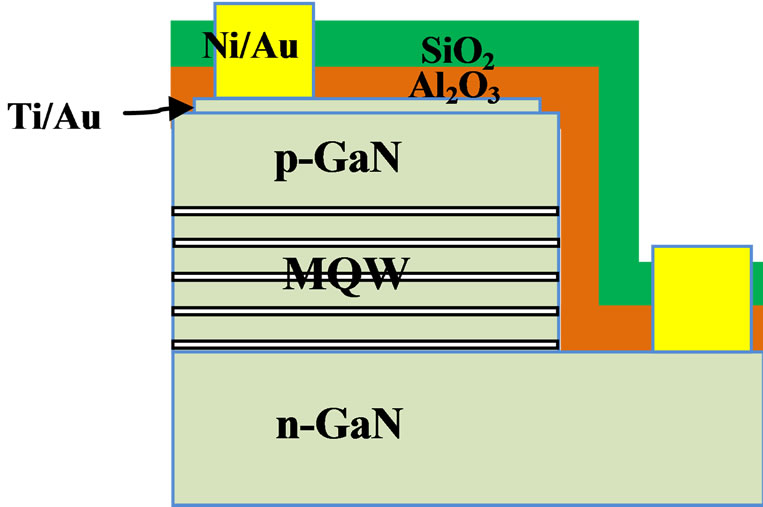
Figure 1(a) shows the schematic LED configuration investigated in this work. The layer structure was grown on the patterned sapphire substrate (PSS) by metal-organic chemical vapor deposition (MOCVD). The blue LED structure contains low temperature grown GaN buffer layer, un-doped GaN layer, Si doped n-GaN layer, InGaN/GaN multi-quantum well active layer and Mg doped p-GaN cladding layer. The composition and thickness of InGaN/GaN multi-quantum well active layer was opti-
 (a)
(a)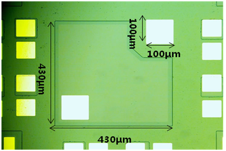 (b)
(b)
Figure 1. The schematic of the LED configuration investigated in this work (a); and the fabrication of the 430 μm × 430 μm size real LED chip (b).
mized for emission wavelength of ~460 nm. Figure 1(b) shows the fabricated LED chip with size of 430 μm × 430 μm.
The window for n-electrode was first defined by dry etching and a transparent electrode consisting of Ni/Au (50 Å/50 Å) was deposited on p-GaN layer, which was followed by rapid thermal annealing at 500˚C (at N2/O2 ambient) for ohmic contact between the transparent electrode and p-GaN top layer. Thick Ti/Au bonding pads with thickness of 300 Å/4000 Å was then deposited. The double dielectric stack layer, which consists of 5 nm-thick Al2O3 layer [15] deposited by plasma-enhanced atomic layer deposition (PEALD) and 50 nm-thick SiO2 layer deposited by plasma-enhanced chemical vapor deposition (PECVD), was sequentially deposited on the surface of the LED to complete the fabrication process. The PEALD method has the advantages such as an excellent uniformity, a high quality film density, a controllability of atom level thickness and the perfect surface step coverage for the LED structure due to the self-limiting deposition characteristic. A gas phase reaction can be suppressed among the injected reactant. Therefore, a thin film layer is formed by a saturated surface reaction therefore the low temperature deposition is possible. In addition, to evaluate the interface trap density between SiO2 or Al2O3 layer and p-GaN layer, the MOS capacitors with anode pattern of 300 µm diameter and virtual ground contact [16] were also fabricated. For comparison, three different LEDs were also prepared; 5 nm-thick single Al2O3-passivated, 50-nm thick single SiO2-passivated, and non-passivated LED.
3. Optimization of Double Dielectric Stack Layer
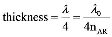
To maximize the optical output power, the refractive index and the thickness of a dielectric layer, were estimated from the concept based on the Fresnel reflection for the antireflection. The Fresnel reflection at the interface can be reduced to zero, assuming normal incidence, when an anti-reflective dielectric layer is inserted between air and semiconductor, which has the following relations:
 (1)
(1)
and
 (2)
(2)
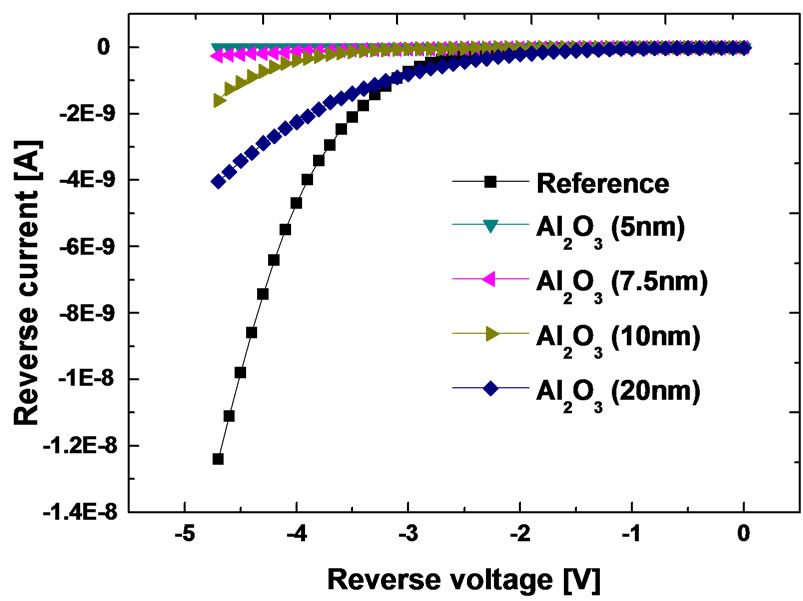
where nAR is a refractive index of anti-reflection layer, nS is a refractive index of semiconductor, nA is a refractive index of air, and λ is wavelength, respectively. The estimated refractive index and the thickness of an antirefraction layer is 1.55 and ~70 nm, respectively, when the semiconductor is GaN and the emission wavelength λ is 460 nm. To obtain nAR of 1.55 with double dielectric stack layer, such as Al2O3 (refractive index of 1.77)/SiO2 (refractive index of 1.46) investigated in this work, the thickness ratio between two dielectric layers is approximately 7(SiO2):3(Al2O3), which approximately corresponds to the SiO2 thickness of 50 nm and the Al2O3 thickness of 20 nm. However, the 5 nm-thick Al2O3 layer was used for the double layer in this work, instead of the calculated value of 20 nm because the reverse current characteristics of the Al2O3-passivated LED become rapidly degraded as the thickness increases as shown in Figure 2(a) (the leakage current of the 5 and 20 nm thick Al2O3 passivated layer were –3.46 × 10⁻¹¹ A and the 2.21 × 10⁻⁸ A at –5 V, respectively).
The degradation in reverse characteristics is believed to be due to the time dependent plasma damage, where the surface damage increases as the exposure time of the LED surface to the plasma increases during the deposition of dielectric layers. The plasma damage may lead to the formation of lattice defects and/or dangling bonds at near-surface which results in the degradation in output power of LEDs as shown in Figure 2(b) [17,18].
The output power of the LED with 20 nm-thick Al2O3 layer is considerably decreased compared to other LEDs with thinner Al2O3 layer. For this reason, the 5 nm-thick Al2O3 layer was chosen to minimize the plasma damage. Additionally, the 5 nm-thick Al2O3 layer plays a role of not only very effective passivation layer of the LED sur-
 (a)
(a)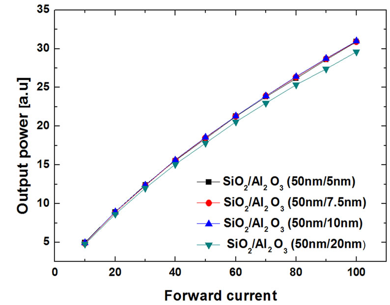 (b)
(b)
Figure 2. The the leakage current characteristics (a) and the output power characteristics (b) of the SiO2 (50 nm)/Al2O3 (5 nm), SiO2 (50 nm)/Al2O3 (7.5 nm), SiO2 (50 nm)/Al2O3 (10 nm), and SiO2 (50 nm)/Al2O3 (20 nm)-passivated LEDs, respectively.
face but also partially anti-reflective layer in combination with 50 nm-thick SiO2 layer even though the thickness is thinner than the calculated value for the anti-reflective layer. As a result, the total thickness for the double dielectric stack layer was optimized as 55 nm to achieve an efficient operation of the LED even though the thickness is not optimized for the maximum anti-reflectivity.
4. Results and Discussion
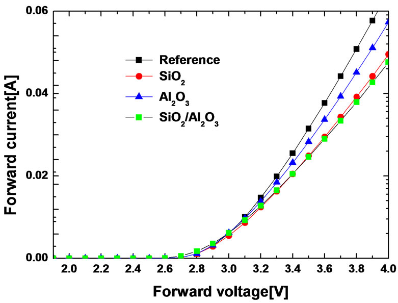
The linear and semi-log I-V characteristics of all fabricated LEDs are shown in Figures 3(a) and (b). The forward voltages measured at 20 mA were approximately 3.31, 3.33, 3.39 and 3.39 V for the non-passivated, the Al2O3-passivated, the SiO2-passivated, and the SiO2/Al2O3- passivated LED, respectively. The forward voltages of the Al2O3, the SiO2 and the SiO2/Al2O3-passivated LEDs are slightly higher than that of the non-passivated LED. It is a little difficult to observe the difference in slopes between LEDs. To clearly see the difference, we compared the I-V curves for only two LEDs in (c) of the figure with the non-passivated LED and the SiO2/Al2O3 double
 (a)
(a)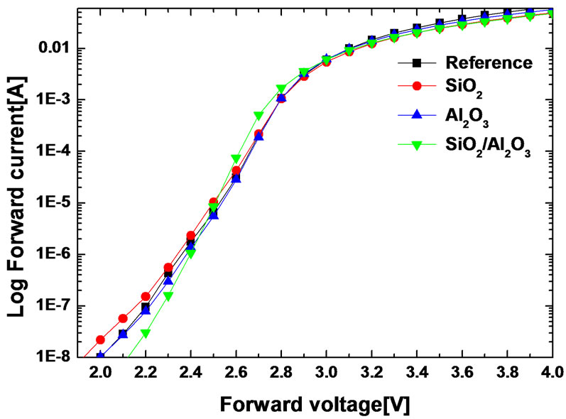 (b)
(b)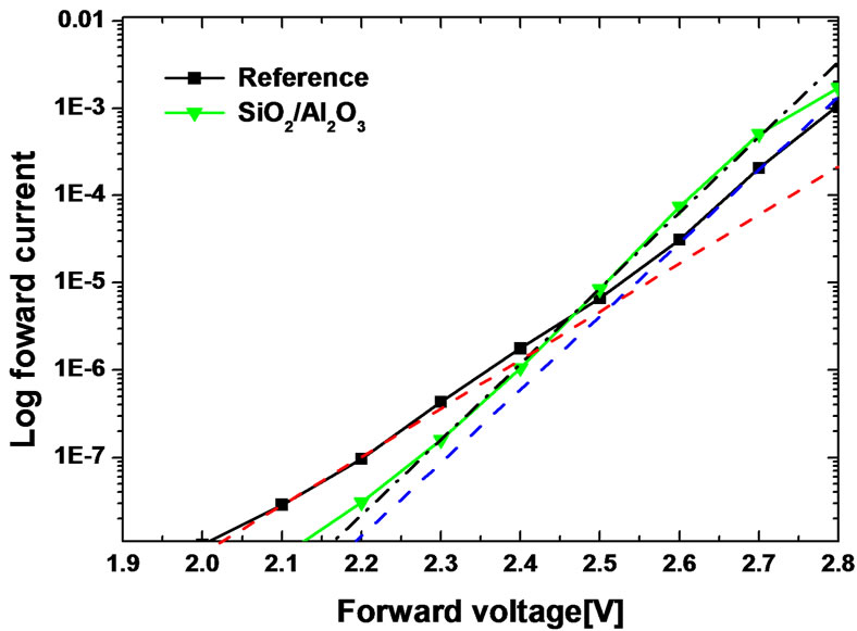 (c)
(c)
Figure 3. The linear and semi-log I-V characteristics for all investigated LEDs at forward bias (a) and (b). To clearly see the difference, we compared the I-V curves for only two LEDs in (b) of the figure with non-passivated LED and the SiO2/Al2O3 double dielectric passivated LED.
dielectric passivated LED. It is apparent that the nonpassivated LED exhibits two characteristic lines, with a small slope at relatively low bias (<2.5 V) caused by which is equivalent to the surface shunt resistance and parasitic diode showing the prematured turn-on [19] as described later. On the other hand, the SiO2/Al2O3 double dielectric passivated LED shows almost one dominant characteristic line with large slope, but the line with small slope disappears except at very low bias below ~2.2 V. This explains that the I-V characteristic of the nonpassivated LED is greatly affected by the existence of the shunt components at surface showing a hump in the curve, while that of the SiO2/Al2O3 double dielectric passivated LED is less affected by these shunt components due to the effective surface passivation of the SiO2/Al2O3 double dielectric layer. Therefore, the SiO2/Al2O3 double dielectric passivated LED exhibits much more improved output power performance due to the decreased nonradiative recombination at surface. However, it is noticed that the SiO2 passivated LED exhibits even worse I-V characteristic than that of the non-passivated one with even further prematured turn-on as shown in the figure. This is probably because the GaN surface becomes easily damaged when the surface is exposed to the plasma during the long deposition time, while the damage becomes minimized for the SiO2/Al2O3 double dielectric passivation because the first thin Al2O3 layer deposited prior to the SiO2 deposition prevents the GaN surface from being damaged. The GaN surface can be passivated with the deposition of the SiO2 layer, which can be resulted in decrease of the effect of the shunt diode at surface. However, the plasma damage introduced during the deposition of the SiO2 layer causes another surface leakage which is responsible for the worse I-V characteristic for the SiO2 passivated LED. The passivation effect of the 5 nm-thick Al2O3 single dielectric layer is not remarkable compared to that of the double dielectric-passivation as shown in the Figure 3(b). This is believed to be due to the insufficient surface passivation caused by nonuniform surface covering of the dielectric layer when the dielectric layer is very thin.
At a higher current level, however, the dielectric passivated LEDs exhibit larger series resistances than the non-passivated LED does as shown in the Figure 4.
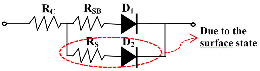
The reason for the increased resistance with dielectric passivation can be understood by adopting an equivalent circuit model, as shown in Figure 5(a), for the LED investigated in this work. The model consists of the main ideal bulk p-n diode (D1), the contact resistance (RC), the bulk series resistance (RSB) mainly due to highly resistive p-type layer, the shunt resistance (RSS), and the parasitic shunt diode (D2) [19]. The shunt diode (D2) and the shunt resistance (RSS) are due to the surface leakage related to the surface states. The I-V characteristics of non-passivated LED can be inferred, considering all intrinsic and parasitic components. The I-V characteristics for D1 (dottedblack line) can be degraded due to RSB and RC (dotted-blue line) as shown in Figure 5(b). The curve for D2 with RSS is also shown as the dotted-green line in the figure. Therefore, the observable I-V characteristics for the non-passivated LED must be sum of the characteristics of the two diodes, shown as the dotted-red line in the figure.

Figure 4. The semi-log I-V characteristics for all investigated LEDs at high forward bias.
 (a)
(a)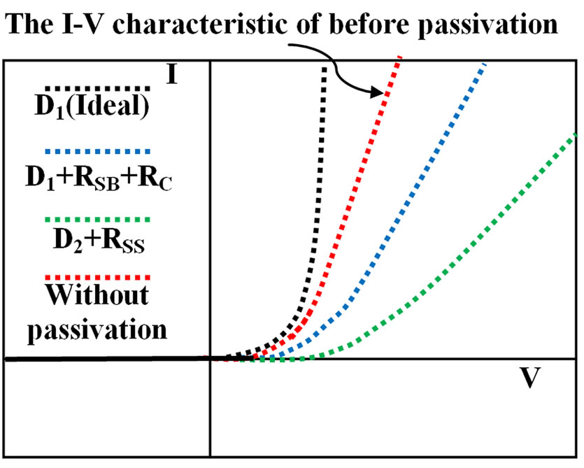 (b)
(b)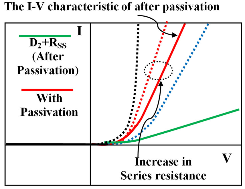 (c)
(c)
Figure 5. The Equivalent circuit model of the LED investigated in this work (a); the I-V characteristics of LEDs without (b); and with (c) passivation.
The I-V characteristics for D1 with RC and RSB do not change even after passivation. However, the portion of D2 with RSS in the I-V characteristics becomes much reduced because the passivation layer greatly decreases the surface state density. This means that the effect of D2 and RSS on the total diode characteristics becomes less which can be visualized as green line in Figure 5(c). Therefore, the I-V characteristics for the passivated LED, obtained from the sum of the characteristics of the two diodes (the broken blue line + the green line), can be drawn as red line in the figure, where the slope of the I-V curve is smaller than that of the I-V curve before the passivation, indicating that the series resistance of the passivated LED is larger than that of the non-passivated LED. The premature turn-on observed for the passivated LED is probably due to the surface leakage, which cannot be fully eliminated by the passivation, and/or additional shunt resistance, caused by plasma damage.
Figure 6 shows the reverse leakage current characteristics for the fabricated LEDs. As shown in the figure, the leakage current of the Al2O3-passivated LED was –3.46 × 10⁻¹¹ A at the –5 V, at least two and three orders lower in magnitude compared to that of the SiO2-passivated LED (–7.14 × 10⁻⁹ A) and the non-passivated LED (–1.9 × 10⁻⁸ A ), respectively.
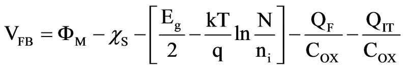
This indicates that the Al2O3 layer is very effective in passivating the exposed GaN surface after dry etch and hence decreases the trap density near the surface, which minimizes the leakage current through the surface of the LED. The trap density at the GaN surface was obtained by estimating the flatband voltage shift of the metalinsulator-semiconductor (MIS) capacitors, which depends on the polarity and the density of charges in the oxide and at the interface [20]. The measured C-V data were compared to the theoretical values using the Equation (3) below and the flatband voltage shift can be calculated.
 (3)
(3)

Figure 6. The LED with Al2O3 layer exhibits at least two and three orders lower in leakage current compared to that with SiO2 layer and without dielectric layer, respectively.
where ΦM is the metal work function, χS is the electron affinity of the semiconductor, Eg is the band gap energy, k is the Boltzmann constant, T is the temperature, q is the elementary charge, N is the doping density, ni is the intrinsic carrier concentration, QF is the density of fixed charges, QIT is the density of interface trap charges, and Cox is the oxide capacitance. The first three terms represent the ideal flatband valtage and the latter two causes the flatband voltage shift which depends on the polarity and the density of charges in the oxide and at the interface. The estimated interface trap density obtained from the QIT are shown in Table 1. The decreased trap density with Al2O3 passivation at the GaN surface leads to decrease in nonradiative surface recombination, which in turn increases the radiative efficiency and hence the output power from the LED.
Figure 7 shows the output powers versus currents for all LEDs studied in this work, which demonstrates the output powers of dielectric-passivated LEDs are higher than that of the non-passivated LED. The output power is 25.8, 26.5, 27.9, and 32.3 for the non-passivated, the SiO2-passivated, the Al2O3-passivated, and the Al2O3/ SiO2-passivated LED at IF = 100 mA, respectively.
The reason for the higher output power for the dielectric passivated LED is because an additional transparent layer with refractive index n on NiAu/GaN as well as on the etched LED surface results in a larger critical angle for the emitted light. It is also noticed that the output power of the Al2O3-passivated LED is slightly higher than
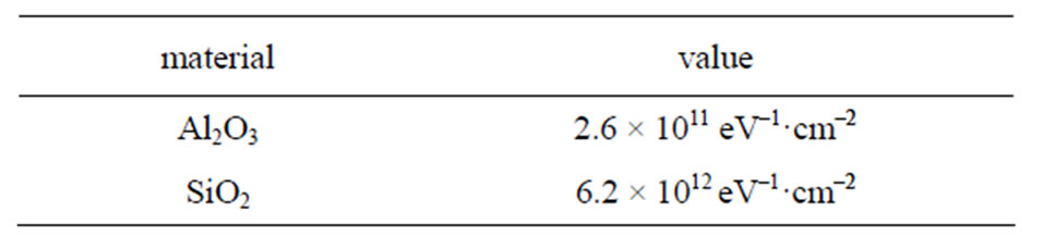
Table 1. Characteristics of interface charge density in GaN MIS structures.
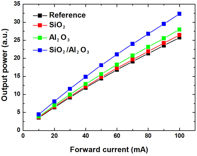
Figure 7. The output power characteristics of the nonpassivated, the SiO2-passivated, the Al2O3-passivated, and the Al2O3/SiO2-passivated LED. The output power of the Al2O3/SiO2-passivated LED exhibits about 25% higher than that of the non-passivated LED.
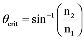
that of the SiO2-passivated LED, which is unexpected and must be discussed, and the double dielectric Al2O3/ SiO2-passivated LED exhibits further enhanced output power. The output power of the SiO2-passivated LED must be higher than that of the Al2O3-passivated LED, because the lower index of the SiO2 layer deposited on the LED plays a role of increasing the light extraction efficiency due to larger critical angle factor as shown in Table 2, which is contrary to the result observed in Figure 7. According to the Snell’s law, the critical angle (θcrit) of total internal reflection is given by
 (4)
(4)
where n1 and n2 are the refractive indices of the semiconductor and air, respectively.
The reason why the Al2O3-passivated LED exhibits higher output power can be explained as follow; the Al2O3 layer covers whole surface of the LED, as shown in Figure 1, including the side-wall surface near the edge of the active quantum well exposed after plasma etching, except the nand p-type contact. This Al2O3 layer effectively passivates the surface of the LED, which not only improves the electrical property of the LED by effectively reducing surface leakage as described before, but also reduces probability of nonradiative recombination through the surface trap and increases the radiative recombination efficiency in the active quantum well near side-wall edge. Furthermore, this passivation layer prevents the reabsorption of the emitted light near the surface regions. The surface passivation with Al2O3 layer, therefore, leads to increase of overall the external efficiency of the LED, even though the extraction efficiency of the Al2O3-passivated LED itself is lower than that of the SiO2-passivated LED.
The output power of the Al2O3-passivated LED can be further increased by depositing additional 50 nm-thick SiO2 layer on the Al2O3 layer to form the SiO2/Al2O3 double dielectric stack layer. The output power of the LED with the double dielectric stack layer exhibits an output power, about 25.4% higher than that of the non-passivated LED and 15.6% higher than that of the Al2O3-passivated LED, respectively. This remarkable enhancement in output power of the LED with double dielectric passivation is because the first Al2O3 layer plays a role of effectively passivating the p-GaN surface and the second lower index SiO2
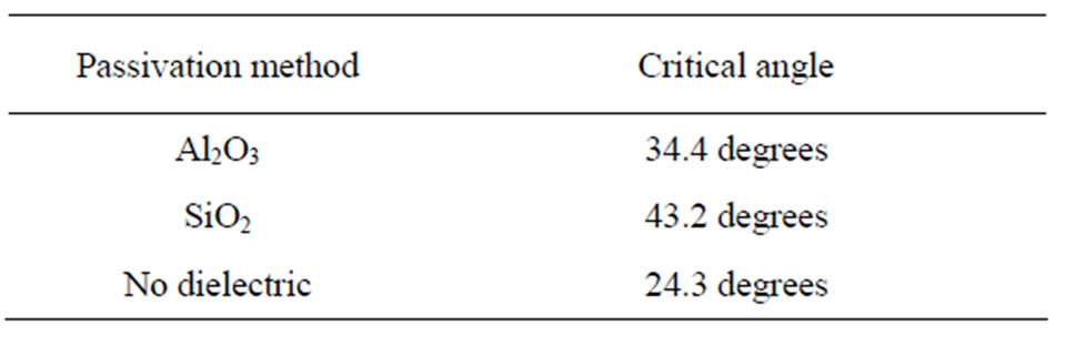
Table 2. The critical angle calculated of dielectric deposited on GaN surface.
layer plays a role of increasing the critical angle of the light emitted from the LED surface. In addition, the effect of the Fresnel reflection are also responsible for this enhancement in output power of the double dielectric passivated LED. Assuming normal incidence of light, the Fresnel power transmittance between GaN and air without any dielectric layer is given by
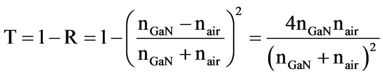 (5),
(5),
when thin dielectric layer, SiO2 or Al2O3, is inserted between GaN and air, the transmittance can be expressed as below, neglecting multiple reflections between dielectric layers for simple calculation.
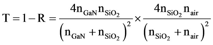 , (6)
, (6)
or
 . (7)
. (7)
Similarly, when double dielectric stack layer, SiO2/ Al2O3, is inserted between GaN and air,
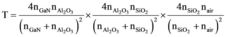 (8)
(8)
where nGaN,  ,
,  , and
, and  are the refractive indices of the GaN, Al2O3, SiO2 and air, respectively. The above equations can be formalized as below:
 (9)
(9)
where i = 1 corresponds to the case without dielectric layer, i = 2 corresponds to the case with single dielectric layer (SiO2 or Al2O3), and i = 3 corresponds to the case with double dielectric layer (SiO2/Al2O3), respectively. From the above equation, the Fresnel power transmittances of the LED without a dielectric layer, with SiO2, the Al2O3, and Al2O3/SiO2 can be approximately calculated as 83.0%, 90.9%, 90.2%, and 93.5%, respectively. The calculated Fresnel power transmittance of the LED with double dielectric passivation, assuming normal incidence of the light, is approximately 10% higher than that that of non-passivated LED. This factor must be included in the improvement of the output power of the LED with double dielectric passivation, along with the contribution from the enhanced radiative recombination efficiency near side-wall edge as described before, which results in increase in the overall extraction efficiency from the LED.
5. Conclusion
We have proposed a new concept of surface passivation for the GaN-based LED to improve the light extraction efficiency by using SiO2/Al2O3 double dielectric stack layer and investigated its effects on the output power of the LED. The double dielectric stack layer not only effectively passivates the surface of the LED, but also enhances the overall extraction efficiency of the LED. The LED with the SiO2/Al2O3 double dielectric stack layer exhibited about a 25.4% increase in the output power compared to the non-passivated LED.
6. Acknowledgements
This work was supported by Kyungpook National University Research Fund 2012, 2008 Brain Korea 21 (BK21), the National Research Foundation of Korea (NRF) grant funded by the Korea government (MEST) (No. 2012- 0005671, 2012-0000627), R & D program of MKE/ KETEP (2011101050017B, “Development of high efficiency GaN power device for an power grid inverter system”), and WCU (World Class University) program through the Korea Science and Engineering Foundation funded by the Ministry of Education, Science and Technology (R33-10055), and the IT R & D program of MKE/KEIT (10038766, Energy Efficient Power Semiconductor Technology for Next Generation Data Center).
REFERENCES
- T. Fujii, Y. Gao, R. Sharma, E. L. Hu, S. P. Den Baars and S. Nakamura, “Increase in the Extraction Efficiency of GaN-Based Light-Emitting Diodes via Surface Roughening,” Applied Physics Letters, Vol. 84, No. 6, 2004, pp. 855-857. doi:10.1063/1.1645992
- C. M. Yang, D. S. Kim, S. G. Lee, J. H. Lee, Y. S. Lee and J. H. Lee, “Improvement in Electrical and Optical Performances of GaN-Based LED with SiO2/Al2O3 Double Dielectric Stack Layer,” IEEE Electron Device Letters, Vol. 33, No. 4, 2012, pp. 564-566. doi:10.1109/LED.2012.2185675
- H.-W. Huang, C. C. Kao, J. T. Chu, S. C. Wang and C. C. Yu, “Improvement of InGaN-GaN Light-Emitting Diode Performance with a Nano-Roughened p-GaN Surface,” IEEE Photonics Technology Letters, Vol. 17, No. 5, 2005, pp. 983-985. doi:10.1109/LPT.2005.846741
- C. M. Tsai, J. K. Sheu, W. C. Lai, Y. P. Hsu, P. T. Wang, C. T. Kuo, C. W. Kuo, S. J. Chang and Y. K. Su, “Enhanced Output Power in GaN-Based LEDs with Naturally Textured Surface Grown by MOCVD,” IEEE Electron Device Letters, Vol. 26, No. 7, 2005, pp. 464-466. doi:10.1109/LED.2005.851243
- M. Y. Hsieh, C. Y. Wang, L. Y. Chen, T. P. Lin, M. Y. Ke, Y. W. Cheng, Y. C. Yu, C. P. Chen, D. M. Yeh, C. F. Lu, C. F. Huang, C. C. Yang and J. J. Huang, “Improvement of External Extraction Efficiency in GaNBased LEDs by SiO2 Nanosphere Lithography,” IEEE Electron Device Letters, Vol. 29, No. 7, 2008, pp. 658-660. doi:10.1109/LED.2008.2000918
- J. H. Lee, J. T. Oh, S. B. Choi, Y. C. Kim, H. I. Cho and J. H. Lee, “Enhancement of InGaN-Based Vertical LED with Concavely Patterned Surface Using Patterned Sapphire Substrate,” IEEE Photonics Technology Letters, Vol. 20, No. 5, 2008, pp. 345-347. doi:10.1109/LPT.2007.915648
- J. H. Lee, J. T. Oh, Y. C. Kim and J. H. Lee, “Stress Reduction and Enhanced Extraction Efficiency of GaNBased LED Grown on Cone-Shape-Patterned Sapphire,” IEEE Photonics Technology Letters, Vol. 20, No. 18, 2008, pp. 1563-1565. doi:10.1109/LPT.2008.928844
- C. F. Shen, S. J. Chang, W. S. Chen, T. K. Ko, C. T. Kuo and S. C. Shei, “Nitride-Based High-Power Flip-Chip LED with Double-Side Patterned Sapphire Substrate,” IEEE Photonics Technology Letters, Vol. 19, No. 10, 2007, pp. 780-782. doi:10.1109/LPT.2007.896574
- S. H. Huang, R. H. Horng, K. S. When, Y. F. Lin, K. W. Yen and D. S. Wuu, “Improved Light Extraction of Nitride-Based Flip-Chip Light-Emitting Diodes via Sapphire Shaping and Texturing,” IEEE Photonics Technology Letters, Vol. 18, No. 24, 2006, pp. 2623-2625. doi:10.1109/LPT.2006.886823
- O. B. Shchekin, J. E. Epler, T. A. Trottier, T. Margalith, D. A. Steigerwald, M. O. Holcomb, P. S. Martin and M. R. Krames, “High Performance Thin-Film Flip-Chip InGaNGaN Light-Emitting Diodes,” Applied Physics Letters, Vol. 89, No. 7, 2006, Article ID: 071109. doi:10.1063/1.2337007
- S. J. Wang, K. M. Usang, S. L. Chen, Y. C. Yang, S. C. Chang, T. M. Chen, B. W. Liou and C. H. Chen, “Use of Patterned Laser Liftoff Process and Electroplating Nickel Layer for the Fabrication of Vertical-Structured GaNBased Light-Emitting Diodes,” Applied Physics Letters, Vol. 87, 2005, Article ID: 011111. doi:10.1063/1.1993757
- H. W. Huang, C. H. Lin, Z. K. Huang, K. Y. Lee, C. C. Yu and H. C. Kuo, “Improved Light Output Power of GaN-Based Light-Emitting Diodes Using Double Photonic Quasi-Crystal Patterns,” IEEE Electron Device Letters, Vol. 30, No. 11, 2009, pp. 1152-1154. doi:10.1109/LED.2009.2029985
- M. F. Schubert, F. W. Mont, S. Chhajed, D. J. Poxson, J. K. Kim and E. F. Schubert, “Design of Multilayer Antireflection Coatings Made from Co-Sputtered and LowRefractive-Index Materials by Genetic Algorithm,” Optics Express, Vol. 16, No. 8, 2008, pp. 5290-5298. doi:10.1364/OE.16.005290
- J.-Q. Xi, M. F. Schubert, J. K. Kim, E. F. Schubert, M. Chen, S.-Y. Lin, W. Liu and J. A. Smart, “Optical ThinFilm Materials with Low Refractive Index for Broadband Elimination of Fresnel Reflection,” Nature Photonics, Vol. 1, No. 3, 2007, pp. 176-179.
- S.-J. So and C.-B. Park, “Improvement of Brightness with Al2O3 Passivation Layers on the Surface of InGaN/GaNBased Light-Emitting Diode Chips,” Thin Solid Film, Vol. 516, No. 8, 2008, pp. 2031-2034. doi:10.1016/j.tsf.2007.07.143
- C. Ostermaier, H.-C. Lee, S.-Y. Hyun, S.-I. Ahn, K.-W. Kim, H.-I. Cho, J.-B. Ha and J.-H. Lee, “Interface Characterization of ALD Deposited Al2O3 on GaN by CV Method,” Physica Status Solidi, Vol. 5, No. 6, 2008, pp. 1992-1994.
- Y. Li, X. Y. Yi, X. D. Wang, J. X. Guo, L. C. Wang, G. H. Wang, F. H. Yang, Y. P. Zeng and J. M. Li, “Plasma Induced Damage in GaN-Based Light Emitting Diodes,” SPIE Proceedings, Vol. 6841, 2007, Article ID: 68410x. doi:10.1117/12.759809
- H. S. Yang, S. Y. Han, K. H. Baik and S. J. Pearton, “Effect of Inductively Coupled Plasma Damage on Performance of GaN-InGaN Multiquantum-Well Light-Emitting Diodes,” Applied Physics Letters, Vol. 86, 2005, Article ID: 102104. doi:10.1063/1.1882749
- E. F. Schubert, “Light-Emitting Diodes,” 2nd Edition, Cambridge University Press, Cambridge, 2006. doi:10.1017/CBO9780511790546
- K. Matocha, R. J. Gutmann and T. P. Chow, “Effect of Annealing on GaN-Insulator Interfaces Characterized by Metal-Insulator-Semiconductor Capacitors,” IEEE Transactions on Electron Devices, Vol. 50, No. 5, 2003, pp. 1200- 1204. doi:10.1109/TED.2003.813456