World Journal of Nuclear Science and Technology
Vol.2 No.4(2012), Article ID:23799,7 pages DOI:10.4236/wjnst.2012.24027
New Method for Diagnostics of Ion Implantation Induced Charge Carrier Traps in Microand Nanoelectronic Devices
1Physics Department, International Islamic University, Kashmir Highways, Islamabad, Pakistan.
2Physics Division, Directorate of Science, Institute of Nuclear Science and Technology, Islamabad, Pakistan
Email: ranamssa@yahoo.com, rana@alumni.nus.edu.sg, mukhtar.ahmedrana@manchester.ac.uk
Received August 14, 2012; revised September 15, 2012; accepted September 25, 2012
Keywords: Semiconductors; Ion Implantation; Defects; Dust Acoustic Waves; Deep Level Transient Spectroscopy; Electron-Hole Plasma; Nanoelectronics
ABSTRACT
An important problem of defect charging in electron-hole plasma in a semiconductor electronic device is investigated using the analogy of dust charging in dusty plasmas. This investigation yielded physical picture of the problem along with the mathematical model. Charging and discharging mechanism of charge carrier traps in a semiconductor electronic device is also given. Potential applications of the study in semiconductor device technology are discussed. It would be interesting to find out how dust acoustic waves in electron-hole plasma in micro and nanoelectronic devices can be useful in finding out charge carrier trap properties of impurities or defects which serve as dust particles in electron-hole (e-h) plasma. A new method based on an established technique “deep level transient spectroscopy” (DLTS) is described here suggesting the determination of properties of charge carrier traps in present and future semiconductor devices by measuring the frequency of dust acoustic waves (DAW). Relationship between frequency of DAW and properties of traps is described mathematically proposing the basis of a technique, called here, dust mode frequency deep level transient spectroscopy (DMF-DLTS).
1. Introduction
During the fabrication, defect or particulate contamination of microelectronic device structures is a serious concern. It can be due to unwanted growth on growth reactor walls or impurities in supply of atomic species in the reactor. Extended defect structures are also formed in different semiconductors used in electronic devices during ion implantation. Extended structures in ion implanted Sb doped Ge (Ge: Sb) form extended defect structures which show high thermal stability and also transform to other defect phases rather than repair. These defects have fatal effects on transport of charge carriers in semiconductor thin films used in electronic devices, which makes knowledge about them important [1-4]. Due to limitation of carrier mobility in Si, Ge has emerged as a key ingredient material for fabrication of a new generation of ultrafast devices in the regime of tens of gigahertz. Ion implantation can be used to write a network of devices on a semiconductor wafer due to possibility of controlled implantation beam size and energy, and masking of the target wafer.
Elemental implantation defects, especially charge carrier traps, and their electronic implications in Ge and similar materials have not been understood with sufficient details, so a comprehensive understanding of properties of defects (vacancies and self-interstitials) in Ge and related materials, and their interactions with impurity atoms is still required [4-7]. These elemental defects join impurities in implanted/doped semiconductors to form defect clusters which act as charge carrier traps. A generalized model for charging and discharging of defects in semiconductor electronic devices is presented here along with its perspective applications.
2. A Model of Defect/Impurity Charging
2.1. Physical Picture
In a perfect crystal of, say, Ge or Si, all the atoms are at their lattice sites and do not have ability to trap additional charge carriers. If impurities are introduced in a perfect crystal, they get ability to trap charge carriers. It may be noted that self interstitial and vacancies are also defects and can trap charge carriers. In real crystalline structure grown for use in devices, contain a variety of defects and sometimes form defect clusters. These clusters are normally composed of vacancy-dopant or interstitial-dopant clusters. These extended clusters can trap a considerable fraction of electrons or holes present in the active volume of a device.
It is thought that these types of extended defect clusters are present in N-type Ge and prevent the feasibility of high speed electronic devices. Depending upon crystal and dopant, preset defect clusters can trap electrons or holes depending on the coulomb potential around defect, impurities or a defect cluster. Electron-hole plasmas are found in electronic devices crystals exposed to optical excitations etc. Defect clusters are exposed to electron and hole currents due to which they are charged. Defect charging in semiconductors is quite complex. After charging processes end, charged defects start discharging naturally. Charging/discharging of defect clusters in semiconductor devices are important and affect performance of devices. Charging and discharging of defects can be used for characterization of charge carrier traps in micro and nanoelectronic devices. Behaviour of deep level traps, which forms the basis for DLTS technique, is described by a schematic in Figure 1 showing electron and hole traps in a semiconductor. Capture & emission by deep-level traps in a semiconductor. DLTS makes use of the measurement of the depletion region of a simple semiconductor electronic device, normally, a Schottky diode. In such a measurement, the regular reverse polarization of the diode is modified by the probing voltage pulse, resulting in the flow of carriers from the bulk to the measurement region, charging the defects or traps. After the pulse ends, thermal emission of carriers from the traps produces the capacitance transient in the device, called the DLTS signal.
2.2. Mathematical Model
Suppose an electron-hole plasma is generated in an electronic device with electron density as ne and hole density nh For simplicity, we assume here extended defect clusters capable of trapping a considerable number of electrons. We consider a case of net electron trapping or negatively charged defects in a semiconductor device. The model situation resembles the typical case of ion implanted Ge:Sb. For the simplicity, we assume that at the time of generation of electron-hole plasma, ne – nh. In implanted Ge:Sb, highly stable vacancy-antimony-Ge clusters (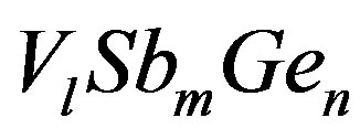 ) are present which are thought to be electron traps in this n-type Ge. These extended defect clusters get charged like dust particles and grains in electron-ion plasma. Let the density of defect cluster or dust grain in e-h plasma, generated in the above mentioned device, is nd.
We further assume here that densities of electrons and holes are below the limit at which inter particle distance becomes lower than de Broglie wavelength of any specific specie which assures that that the case e-h plasma being discussed here is of classical nature. If we take charge of electron as –e, hole as +e and defect or dust grain s – Zd·e, the well-known condition of charge neutrality can be written as below:
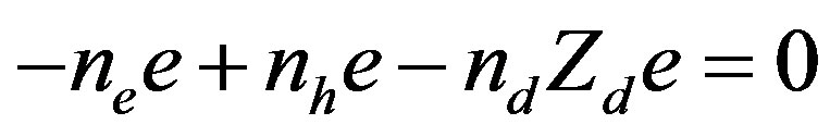 (1)
(1)
Using simple algebra,
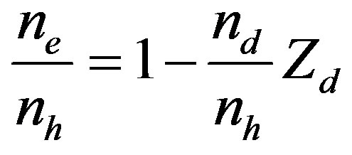 (2)
(2)
For any practical device, defect grain density is much lower than densities of electrons and holes, so the number
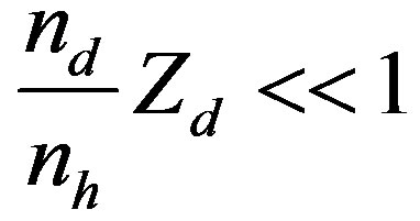
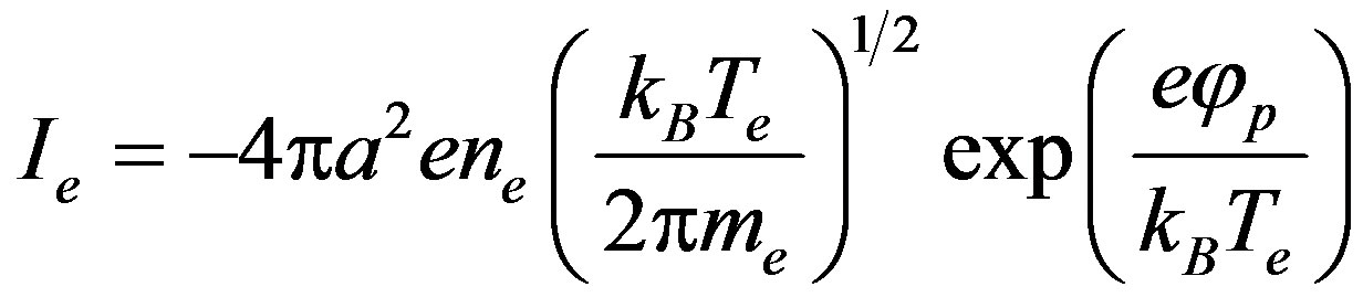
which is the case of isolated dust or defect grains [8-11]. It may also be noted that in present devices defect grains can be only up to a few nanometer size. Maximum charge on defect depends upon defect structure and its size. A isolated defect or dust grain in e-h plasma attains a floating potential  which is determined by electron repulsion and hole collection in case of net negative charging of defects. The electron current responsible for depositing electrons on the defect is given by,
 (3)
(3)
where me and Te are electron effective mass and temperature, and  is the radius of the equivalent sphere of defect grain. The hole current compensating electron charging of a defect is given by,
 (4)
(4)
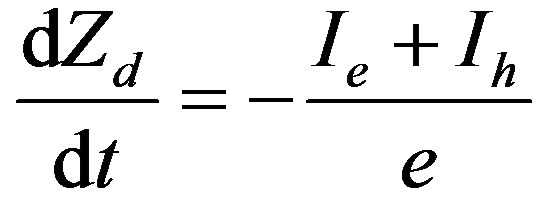
where mh and Th are hole effective mass and temperature. For further details of equations (3), (4), please see Refs. [8-12]. The charging equation of a negatively charged grain can be written as below, [8-10].
 (5)
(5)
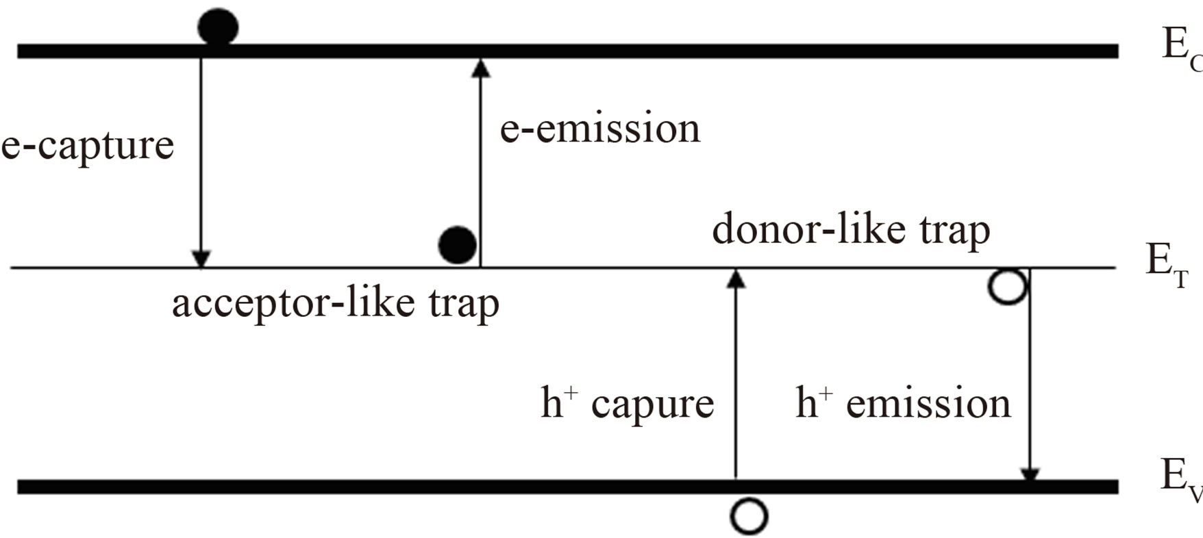
Figure 1. Energy band diagram for a semiconductor with deep-level traps. EC is lower edge of the conduction band while EV is the upper edge of the valence band.
Case of hole or positive charging of defects can be described using a simple analogy and comparison between electrons and holes.
2.3. Mechanism of Charging and Discharging of Electron Traps in an Electronic Device
Electron traps are centers in a semiconductor capable of trapping electrons with a certain binding energy. Traps cause power dissipation and reduce conductivity of the device. When electrons and holes are present in the form of a plasma in an electronic device, dust or defect grains are exposed to both electron (Te) and hole (Th) currents. These currents simultaneously charge and discharge defect grains. When e-h plasma is first generated (t = 0) in an electronic device, a charging transient is produced after which charging and discharging perturbation continues until the device operation ends (end of e-h pair generation). After this, a discharging transient is produced in which electrons are released due to thermal agitation and thermally generated holes. UV light can also produce discharging through photoelectron emission.
3. New Method for the Diagnostics of Charge Carrier Traps in a Microand a Nanoelectronic Device
The frequency ω of dust acoustic mode in electron ion plasma, with dust charged as negative, is given by [8-10],
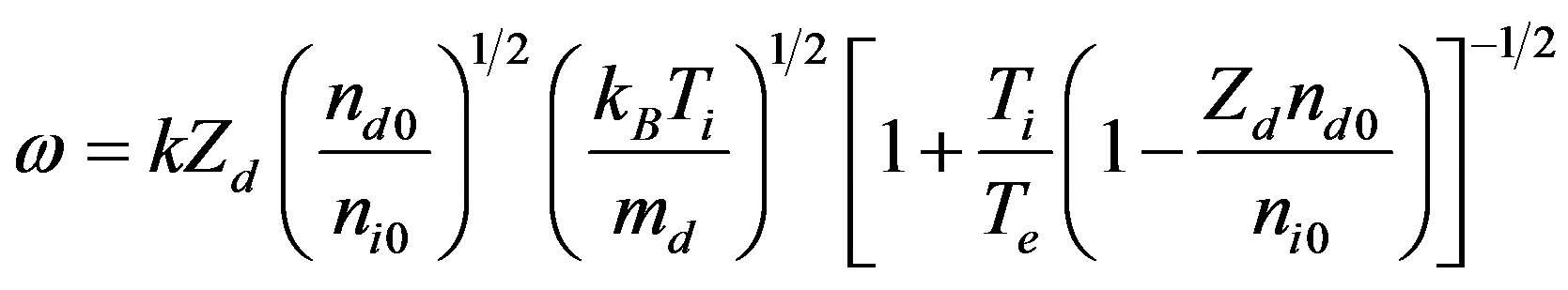 (6)
(6)
where k is the wavenumber, kB is the Boltzman constan, Zd is charge on the dust, nd0 and ni0 are, respectively, equilibrium dust and ion densities, mi and md are, respectively, ion and dust masses, Te and Ti are electron and ion temperatures respectively and e is the electronic charge. With take the case of semiconductor device working at room temperature and having low electron and hole densities (due to low doping level) so that plasma behavior is classical. With charge traps or dust in the device, the above equation the following form by replacing ion parameters with hole parameters,
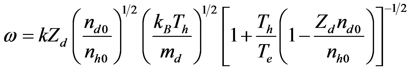 (7)
(7)
Now, mh and nh0 are, respectively, hole mass and equilibrium density. Dust particles in e-h plasma are impurities or defect clusters which can be positively charged, negatively charged or neutral. Dust particles in e-h plasma can have a range of mass and mobility coefficient as they can be free or loosely or strongly bound to the host lattice structure. So, dust model in e-h plasma in electronic devices can be of quite complex nature.
Here, following questions about e-h-dust plasma in semiconductor devices are investigated. What can be the nature of dust modes in e-h-dust plasma in semiconductor devices? Can these dust modes be useful in diagnostics of present or future micro or nanoelectronic devices? What can be the practical method of utilizing dust modes in diagnostics of semiconductor devices?
Dust particles (impurities or defects) in a semiconductor device act as electron or hole traps depending upon its electronic structure. If a pulse of electrons or holes is injected into a semiconductor device, as in a charge carrier trap characterization technique DLTS [13-15], these dust particles will be charged with electrons are holes. After the charge carrier feeding pulse ends, charged defects or dust particles will start discharging and it will continue until dust particles or defects reach their equilibrium charge. Dust mode frequency will also change as dust charge changes with time. This changing mode frequency with time is given by the following,
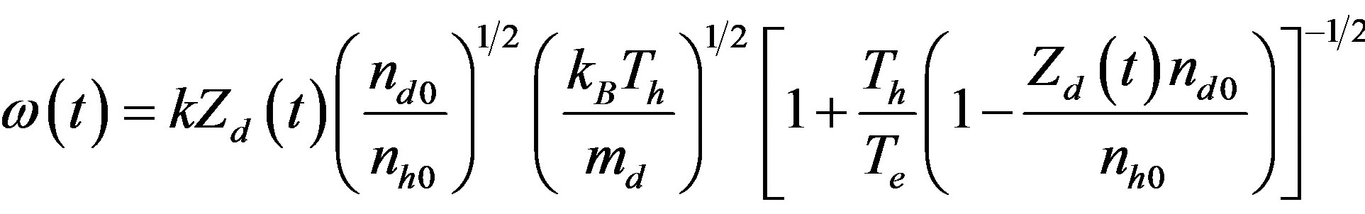 (8)
(8)
In DLTS technique, the device is biased at a reverse bias VR at which the bias is pulsed by a trap filling pulse VP for a time tp. Filled defect states start emptying, when bias returns back to VR, and that results in a capacitance transient. Filling pulse is applied in a series and the varying capacitance of the diode  is given by [16],
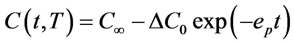 (9)
(9)
where  is the equilibrium capacitance value at reverse voltage,
  is the lowering of
  at t = 0 and ep is the hole emission coefficient. The above equation will be valid for electron traps with ep replaced with en (the electron emission coefficient) and
  is the rise of
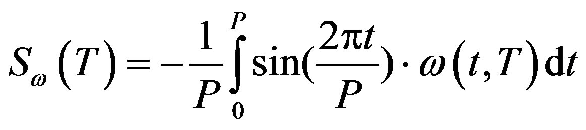
  at t = 0. DLTS spectrum is generated by applying a sine-function correlation with period P to
  as,
as,
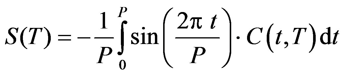 (10)
(10)
The above procedure is applied to determine fundamental Fourier component of the transient,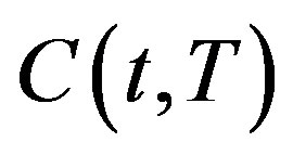 . For exponential transients, the period P, the emission coefficient ep and Tmax for which
  shows a maximum, are related as [17]
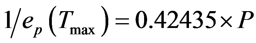 (11)
(11)
By choosing different appropriate values of period P, corresponding values of ep and Tmax can be determined for a specific transient  corresponding to a particular hole trap.
As clear from Equation (3), the frequency of dust would depend on varying charge Zd of dust particles in the same way as  during dust or trap discharge after the application of the filling pulse. So, dust mode frequency transient
  for the same hole trap as in Equation (4), an analogue to capacitance transient
 , can be defined as,
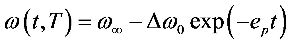 (12)
(12)
where  and
and  are, respectively, equilibrium dust mode frequency and full magnitude of the frequency transient at t = 0. In the same way as in Equation (5), dust mode frequency DLTS or DMF-DLTS signal,
  , can be generated by applying the correlation sine-function as in Equation (5),
 (13)
(13)
DMF-DLTS will show a set of peaks of  signal, each corresponding to a particular dust specie. This spectrum of peaks will be similar to a DLTS spectrum (Figure 2) with different DLTS peaks, with peak parameters carrying finger prints of dust species. Once dust mode frequency
  and change
  are measured, further details of experimental and analysis aspects of implementation of this new DLTS can be seen by a selected studies available in the common literature [13-19].
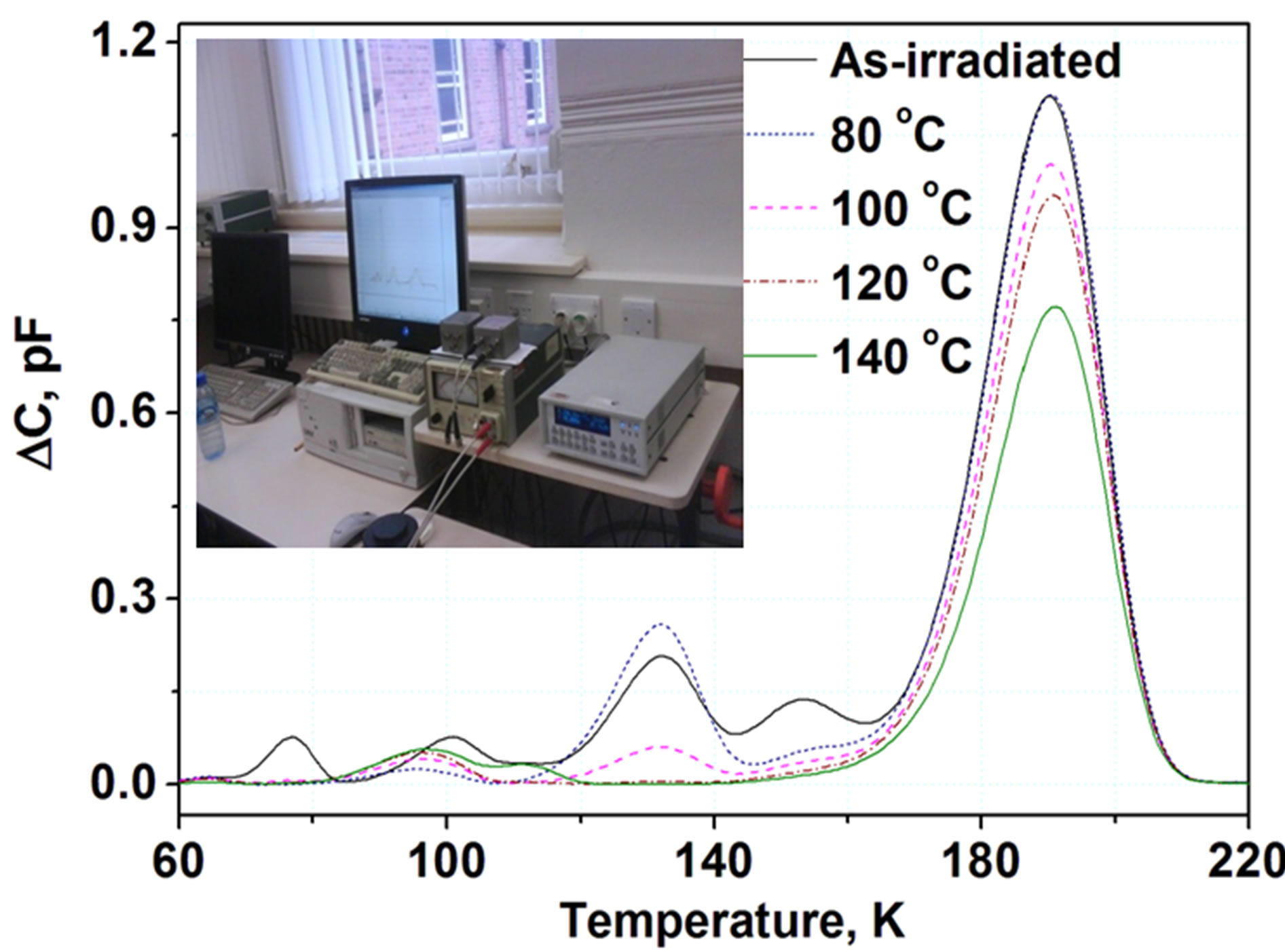
Figure 2. DLTS signal showing traps caused by the electron irradiation induced in Sb-doped (r » 20 W×cm) Ge sample for the filling pulse of –0.5 V. Reverse bias –5 V and filling pulse duration of 10ms were used. As a simple rule, each peak represents an electronically active trap. Measurements of the same sample annealed for 30 m at temperatures of 100˚C - 220˚C are also shown which reduction or evolution of traps due to thermal treatment. The inset shows the measurement system at Microelectronics & Nanostructures Group, Electrical and Electronic Engineering, UMIST, University of Manchester, Manchester M60 1QD, UK University of Manchester, UK. These results were collected with the help of A. R. Peaker, V. P. Markevich and I. D. Hawkins.
4. Potential Applications and Discussion
The present investigation provides the essential information for understanding charging/discharging of defects in semiconductor electronic devices using transient and steady state conditions of operation. It is well known that switching on and off of a range of electronic devices affects their life. Charging and discharging currents produced, respectively, in switching on and off of an electronic devices affect its quality life.
Deep level transient spectroscopy [13-15] makes use of charging and discharging capacitance transients for characterization of charge carrier traps in a semiconductor electronic device. According to this study small scale charging and discharging perturbations continue even during steady state operation of devices. These perturbations would have higher magnitude and intensity if an electronic devices operation different operational stages. These perturbations produce a fluctuating filed in the device. Fluctuating fields can have more deleterious effects on the operating device, especially if the fluctuation frequency is high.
Here, we classify defects in a semiconductor electronic device into three classes which are electronically inactive defects, electronically static defects and electronically dynamic defects. Electronically dynamic defects continue producing charging and discharging transients in an operating device and are most undesirable. Electronically inactive defects only decrease active volume of the device and have minimum undesirable effects whereas electronically static defects trap charge carriers but do not produce negligible charging and discharging transients after getting charged at start up of the device. The work presented here in conjunction with the fundamental plasma work [20,21] may lead to applications in the field of Nanotechnology [22,23] and nuclear instruments and methods [24-27].
Figure 3 is a pictorial view of findings of the paper. Physical significance of charge carrier traps in a semiconductor is shown graphically at the right bottom of the figure. Immediately above it shown is a physical process of bending of a crystal (as a pictorial view) which can introduce charge carrier traps in a crystal.
5. Conclusion
Defects are charged due to electron and hole currents. Meaningful charging/discharging continues until . Start up of a device and in some conditions the condition
  is not fulfilled, so charge fluctuations continue casing energy dissipation which is undesirable due to the problem of decreased efficiency. Energy dissipation also limits life of the device. Using this investigation, defects in semiconductor electronic devices are classifieds into three groups, electronically inactive defects,
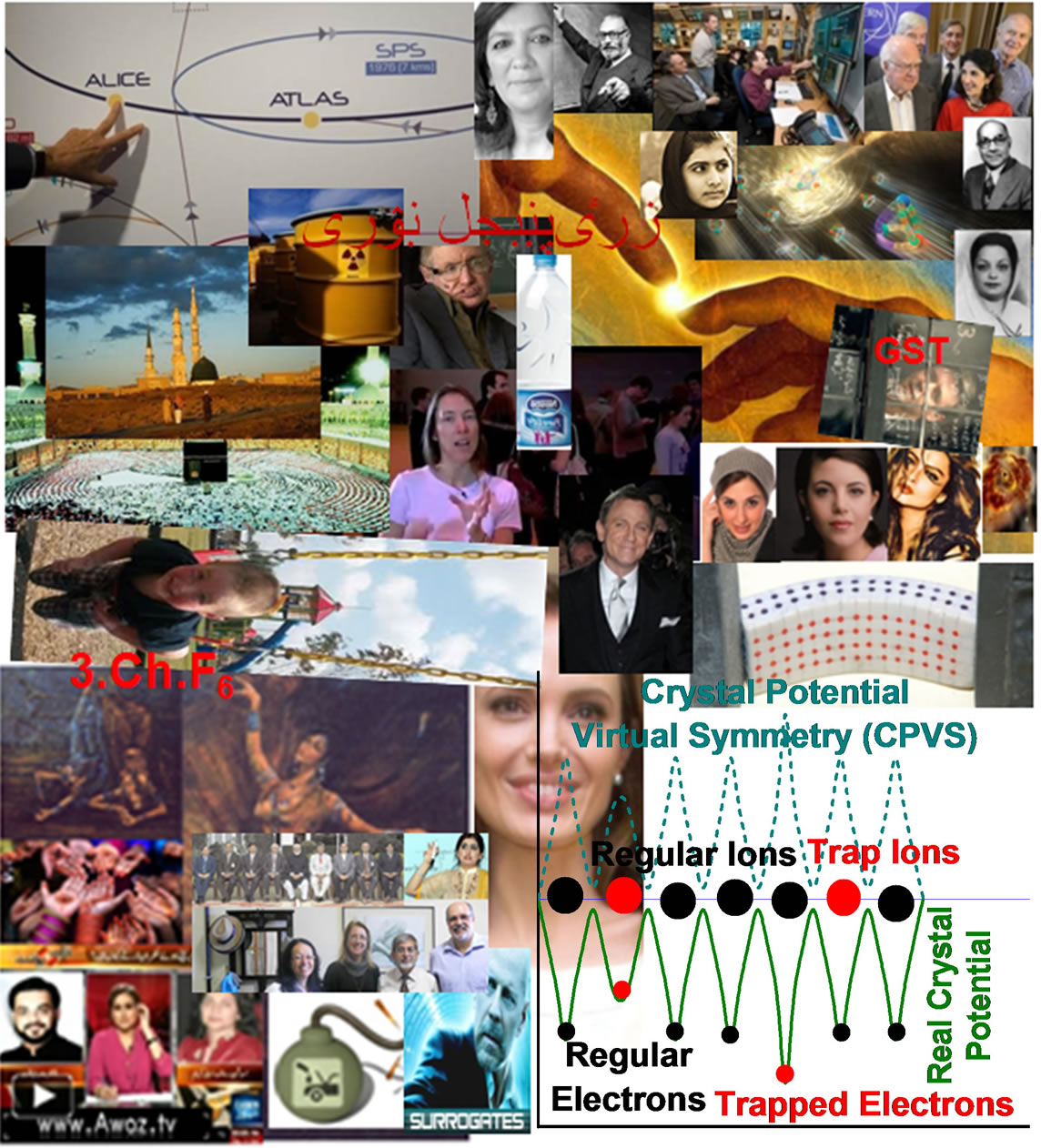
Figure 3. This is a pictorial view of the findings reported in the paper. For the better apprehension of the reader, some aesthetic/geometric Visualization of traps are shown. Right bottom (RB) is geometric visualization of charge carrier traps (here electrons shown) in the form of a plot. These traps have an analogy with massive dust particles in traditional and fullerene plasma [9,10]. Above RB plot, a pictorial view of bending crystal model is show. Bending of a crystal can possibly create traps in it. Other than RB plot, typical mounty or mounted pictures are taken freely available on the web. Leading sources of the pictures are webpages of FermiLab Today (US), CERN (Switzerland), Dawn News (Pakistan), OGRA (Pakistan), PINSTECH/SID Library (PAEC, Islamabad, Pakistan).
electronically static defects and electronically dynamic defects. Electronically dynamic defects are most harmful for semiconductor electronic devices. A new technique DMF-DLTS is proposed here by describing measurement principle of the technique. This new technique combined with conventional and Laplace DLTS techniques can serve as a combination of carrier trap characterization techniques capable of extracting further advanced information about carrier traps in semiconductor devices.
6. Acknowledgements
Generous help regarding “deep level transient spectroscopy” (DLTS) and discussions with Prof. Tony Peaker, Dr. Vladimir Markevich, Dr. Ian Hawkins, Prof. Aimin Song, Miss Sam Aldean, Miss Kerry Plant, Dr. Leszek Majewski, Prof. Bruce Hamilton, Ms. Marie Davies, Dr. Huda El mubarek (Royal Academy of Engineering and EPSRC Research Fellow), Dr. Ahmed El-makadema, Ms. Katy Woolfenden (the Central library) and Prof. Mohamed Missous at the University of Manchester, UK, are gratefully acknowledged. Revealing discussion with Dr. Waqas Masood, Prof. Pervez Hoodbhoy, Mr. Haidar Rizvi, Sughra, Mother Teresa, Haseeb Hasnain, Qamarul Haq and Dr. Nawab Ali about geomagnetic field, solar winds, and Saturn’s rings in links with the space plasma ought to be thanked. Thanks are also for Mr. Asif Osman for morality motivated and philosophical healthy discussions. Helpful and dedicated thoughts sharing of Dr. Shoaib Ahmad (presently at CASP, Church Road, GCU, Lahore) about micro and nanoelectronic devices are respectfully appreciated. This work started as composing of knowledge from distant fields of plasma physics and nanoelectronics which later achieved to be a mature draft/manuscript. The financial help from the HEC, Islamabad (Pakistan) is heart-feelingly acknowledged. The help/discussion with Ms. Ee Jin Teo, Ms. Halen (Philpine), Markus Zmeck, Andrew Bettiol (Australia), Ong Yiew Leung, Abdullah Al Mamun, Abdullah Al Mamun, Shazib Pervaiz, at the National University of Singapore, are appreciated. Thanks are also due for G. Giacomelli, L. Patrizii, V. Togo from the Bologna University; and Vincenzo Guidi, Andrea Mazzolari, the University of Ferrara; Sara Maria Carturan, INFN—Laboratori Nazionali di Legnaro (Italy); G. Schiwietz (Helmholtz-Zentrum Berlin f. Materialien u. Energie, Hahn-Meitner-Platz 1, 14109 Berlin, Germany) and P. L. Grande (Uni. Federal do Rio Grande do Sul, Av. Bento Gonçalves 9500, 91501-970 Porto Alegre, RS, Brazil), Sandro Guedes, Julio Hadler and Eduardo Curvo (Instituto de Fisica Gleb Wataghin, Universidade Estadual de Campinas, UNICAMP, 13083-970 Campinas, SP, Brazil) have been helpful; Nidal Dwaikata, Ghassan Safarinib, Mousa El-hasanb (An-najah National University, Nablus, Jerusalem, Palestine); Shoji Hashimoto, Shin Ugawa, Kazuki Nanko & Koji Shichi (Soil Resources Laboratory, Department of Forest Site Environment, Forestry and Forest Products Research Institute, 1 Matsunosato, Tsukuba, Ibaraki, 305-8687, Japan); K. Stübner, R. C. Jonckheere, L. Ratschbacher (Institut für Geowissenschaften, Technische Universität Bergakademie Freiberg, Sachsen, Germany); Xiangdong Ji (Institute of Nuclear, Particle, Astronomy and Cosmology Offic: Physics Building Rm. 606 (Shanghai Jiatong University, Shanghai, PRC; MIT, USA); Fatih Gerçekcioğlu (Kirikkale University, Turkey); Laureline Bourcier (Institute for Reference Materials and Measurements, Joint Research Center, European Commission, B-2440 Geel, Belgium); Prof. Man Gyun Na (Chosun University, Korea (South)), S. Mostafa Ghiaasiaan Editor, Editor ANE at G. W. Woodruff School of Mechanical Engineering Erskine Love Manufacturing Building Georgia Institute of Technology, Atlanta.
This paper marks the concurrent occurrence of 4 events including Islamic Conference 2012 at the Makkah, Saudi Arabia, the Pakistan’s Independence Day Celebrations (Mubarek), the 2012 Olympics, London, UK, and NASA’s Mars Mission which benefitted me in further shaping my mind. Participation in 2 workshops: 1) Pakistan’s Strategic Needs; 2) The Role of China in Nuclear Power in Pakistan), at NAFDEP, the Pitfalls Waterlanes, the Neelam Silk Route, Islamabad, were beneficial.
Discussion/help/inspiration from individuals/places/ concepts/institutions (local or at places mentioned above, mentioned otherwise) Ahmed Raza Brailvi, Shah Ahmed Noorani, Mufti Mahmood, Hussain Ahmad, Liaqat Balauch, Tahir-ul-Qadri, Haji Abdul Wahab, Pir Pagaro, Ray Wind, Shaukat-Khanum, Naseer-ud-Din Shah, Qari Khushi Muhammad Al-Azahari, Data Nagari, Haroon Rashid, Adnan Kayani, Naheed, Saad Sajid Bashir, Shahid Bilal Butt, Ishtiaq Kashmiry, Razia Butt, Atta-ul-Haq Qasmi, Skill Development Initiative (KINPOE & KANUPP, Karachi), Zafar Shuttle Service, Faiz-ul-Hassan, Khalid Minhas, Nafeesa Nazali, Farhat, Ayesha, Shazia, Serwat, Kanwal, Rahat Bakers, Kalabagh, Nadra, Ada Kidman, Military College Jhelum, Sarai Alamghir; Pakistan Naval Academy, Karachi; Pakistan Air Force Academy, Risalpur: Iqbal, Karsaz, Rashid Minhas, M. M. Alam, Mehran, Bahadur, Maj Aurangzeb, Brig (R) Muhammad Afzal Malik, Lt Col Abdul Qayyum Satti, Capt Shahbaz Anjum, Miss Shazia Tabassum, Miss Aneela Malik, Miss Amber Amin, Mr. Sajjad; Balqis Kaur, Ameer Chak, Bashir, Bajwa, Gujjar, University of Balauchistan, Quetta: Abdul Manan Bazai, Zahid Ali Marwat, Mr. Muhammad Arif, Ms. Faiqa Abdul Hayee, Ms. Faiza Mir. Fida Muhammad Bazai; Faisal, Hina Jeelani, McDonald, KFC, NIM, Asma Jahangir, Veena Malik, Mahreen A. Raja, Naseeb (Narowal), Matiullah/Shafiq, Babar, Rashid, Arshi, Maulvi Malik Mushtaq (Master Teddi, Shakargarh), Aziz, Sorruyya Deendar, Prof. Zaka Ullah, Belal Baaquie, Murray Barrett, Meng Hau Kuok, Nidhi Sharma, Kuldip Singh, Edward Teo, Xuesen Wang, Artur Ekert, B. V. R. Chowdary, Ms. Teo Hoon Hwee, Ms. Zhou Weiqian, Faiza, Fariha Pervez, Sajjad Ali, Komal Rizvi, Abrarul-Haq. Ali Haider, Alamgir, Aman, Yasin Malik, Zaid Bin Annehan, Hamza Tzortzis, Asma Jahangir, Aslam Masih, Muhammad Bashir, Rawla Kote, Azad Kashmir (24 Hours), Aziz Qureshi, Nasreen Qureshi, R.M. Qureshi; Sy Hong Kok (Singapore), Ghazzala, Ashiq Hussain Dogar, Shagufta, Rana Rab Nawaz, Muhammad Saeed, Maria Sultan Bӧhmer Wasti, Sharmila Tagore, Zulfiqar, Saleem, Shikh Zaid Bin Sultan Al Nahian (UAE), Maimoona Murtaza Malik, Nida, Safdar, Sohail, Nichia (Japan), Sajjad Ali, Afnaan, Hasnain, Kainat, Nauman, Sameena, Shafqat, Shaukat Ali Bhatti, Imran, Awais, Bilal, Maaz, Masrur, Shakeel, Syed Noor, Tahira Sayed, Syed Hameed Qaiser, Fareeha Pervez, Shamoon Maseeh, Raheem Shah, Zain, Abrar-ul-Haq, the proposed Mireeza Foundation, PIMS, Islamabad, Urba, Abdullah, Ghannia, Asad, Iqra, Dar-ul-Amman, Naat Khawan Rabeya, Ashiq Anjum, Sana, Tandoori, Lavish Dine, Tariq Dogar, Pak Continental, Gourmet Cola (Lahore), Mukhtar Maseeh, Adnan, Saima, Mohsin, Lubna, A. R. Peaker, University of Pretoria, Republic of South Africa: M Diale, T Hlatswayo, J. Janse van Rensburg, D. Langa, W. Meyer, C. Moji, J. Nel, Claudia Zander, E. A. Meyburgh, P. Chakraborty, J. van der Merwe; Fauzi, Manzoor Hussain, Nuclear Decommissioning Authority (NDA): John Mathiesen, Easton Murray, Elizabeth Atherton; Shahid, Azhar, Dar-us-Salaam (Singapore), Al-Huda Quran & Hadees Academy, Islamabad, Khalid, Jameel, Hafiz, Faisal, Saeed, Riffat, Fasih, Mano, Umar, Farah, Saima, Sidra, Showkat (Sahiwal), Aftab Iqbal (Okara). Javed Chaudhary, Hamid Mir, Irfan Siddiqi, Asma Shirazi, Saleem Safi, R. U. Yusufzai, Shah Rukh Khan, Shehzad Roy, Kareena Kapoor, Baba Nanak, Kabeer, K. K. Khattak, Dr. Karishma (Gujraat), Azhar Mehmood Kayani (AFIC, Rawalpindi), Kamila, LCWU, Lahore:Yasmin Ali, Shafaq Arif, Lubna Mustafa, Rehana Zia; Dalda and Meezan Cook-books, Sardar Abdul Qayyum, Azad Kashmir, PTCL, OGDCL, Daak Khana, Madina Cash & Carry, Makkah Traders, RanaAcademy, Saqib Osman, Muhammad Akhtar, Mushtaq Ahmad. Inspiration from the mind awakening Hamd & Naat writers & reciters/movies/ characters/dramas/books/singers/newpapers/channels/websites, Altaaf Hussain Hali, A Beautiful Mind, The Ugly Truth, Pearl Harbor, Black Rain (Hiroschima, Nagasaki), The Message, Un-Kahe, Ghazi Ilam Din Shaheed, Tere Naam, Shabana, Ram Chand Pakistani, Tere bin Laden, Banjaran, Silsila, Kabhi Kabhi, Heer, Cleopatra, Vizontele, Tears of Gaza, Downfall, Mr. Bean, My Fair Lady, Das Leben der Anderen, Tokio Hotel, Half Plate, Devils on the Doorstep, Dess, Waqt, Time, BBC (Hard talk), Newweek (Fareed Zakaria), Fatmire Bajramaj (Kosovo & Germany), Marco Soggetto (Eni, Milano, Italy), CNN (Christiane Amanpour), Google, Wikipedia, Youtube, Dutsche Welle, VoA, Beijing Radio, Radio Masco, Ranghun, Bol, Radio Pakistan, FM 92.5, ARY Qur’an TV, Geo, Dunya, Dawn, Express News, PTV.
REFERENCES
- F. D. Auret, A. R. Peaker, V. P. Markevich, L. Dobaczewski and R. M.Gwilliam, “High-Resolution DLTS of Vacancy-Donor Pairs in P-, Asand Sb-Doped Silicon,” Physica B: Condensed Matter, Vol. 376-377, 2006, pp. 73-76.
- V. P. Markevich, I. D. Hawkins, A. R. Peaker, K. V. Emtsev, V. V. Litenov, L. I. Murin and L. Dobaczewski, “Vacancy-Group-V-Impurity Atom Pairs in Ge Crystals Doped with P, As, Sb, and Bi,” Physical Review B, Vol. 70, No. 23, 2004, Article ID: 235213.
- H. J. Queisser and E. E. Haller, “Defects in Semiconductors: Some Fatal, Some Vital,” Science, Vol. 281, No. 5379, 1998, pp. 945-950. doi:10.1126/science.281.5379.945
- P. Muret, J. Pernot, T. Teraji and T. Itoh, “Near-Surface Defects in Boron-Doped Diamond Schottky Diodes Studied from Capacitance Transients,” Applied Physics Express, Vol. 1, No. 3, 2008, Article ID: 035003.
- J. Coutinho, S. Oeberg, V. J. B. Torres, M. Barroso, R. Jones and P. R. Briddon, “Donor-Vacancy Complexes in Ge: Cluster and Supercell Calculations,” Physical Review B, Vol. 73, No. 23, 2006, Article ID: 235213. doi:10.1103/PhysRevB.73.235213
- S. Roy and A. Asenov, “Where Do the Dopants Go?” Science, Vol. 309, No. 5733, 2005, pp. 388-390.
- V. P. Markevich, “A Comparative Study of Ion Implantation and Irradiation-Induced Defects in Ge Crystals,” Materials Science in Semiconductor Processing, Vol. 9, No. 4-5, 2006, pp. 589-596. doi:10.1016/j.mssp.2006.08.062
- P. K. Shukla and A. A. Mamun, “Introduction to Dusty Plasma Physics,” Institute of Physics Publishing, Bristol and Philadelphia, 2002.
- W. Masood, H. Rizvi, H. Hasnain and Q. Haque, “Rotation Induced Nonlinear Dispersive Dust Drift Waves Can be the Progenitors of Spokes,” Physics of Plasmas, Vol. 19, No. 3, 2012, Article ID: 032112.
- W. Masood, A. M. Mirza and S. Nargis, “Revisiting Coupled Shukla-Varma and Convective Cell Mode in Classical and Quantum Dusty Magnetoplasmas,” Journal of Plasma Physics, Vol. 76, No. 3-4, 2010, pp. 547-552
- M. S. Barnes, J. H. Keller, J. C. Forster, J. A. O’Neill and D. K. Coultas, “Transport of Dust Particles in GlowDischarge Plasmas,” Physical Review Letters, Vol. 68, No. 3, 1992, pp. 313-316. doi:10.1103/PhysRevLett.68.313
- A. Piel and A. Melzer, “Dusty Plasmas—The State of Understanding from an Experimentalist’s View,” Advances in Space Research, Vol. 29, No. 9, 2002, pp. 1255-1264.
- D. V. Lang, “Recalling the Origins of DLTS,” Physica B, Vol. 401-402, No. 1, 2007, pp. 7-9. doi:10.1016/j.physb.2007.08.102
- D. V. Lang, “Deep-Level Transient Spectroscopy: A New Method to Characterize Traps in Semiconductors,” Journal of Applied Physics, Vol. 45, No. 7, 1974, pp. 3023- 3032. doi:10.1063/1.1663719
- D. V. Lang and L. C. Kimerling, “Observation of Recombination-Enhanced Defect Reactions in Semiconductors,” Physical Review Letters, Vol. 33, No. 8, 1974, pp. 489-492. doi:10.1103/PhysRevLett.33.489
- S. Voss, N. A. Stolwijk, H. Bracht, A. N. Larsen and H. Overhof, “Substitutional Zn in SiGe: Deep-Level Transient Spectroscopy and Electron Density Calculations,” Physical Review B, Vol. 68, No. 3, 2003, Article ID: 035208. doi:10.1103/PhysRevB.68.035208
- D. S. Day, M. Y. Tsai, B. G. Streetman and D. V. Lang, “Deep-Level-Transient Spectroscopy: System Effects and Data Analysis,” Journal of Applied Physics, Vol. 50, No. 8, 1979, pp. 5093-5098. doi:10.1063/1.326665
- S. Q. Wang, F. Lu, Z. Q. Zhu, T. Sekiguchi, H. Okushi, K. Kimura and T. Yao, “Compensating Levels in p-Type ZnSe:N Studied by Optical Deep-Level Transient Spectroscopy,” Physical Review B, Vol. 58, No. 16, pp. 10502- 10509. doi:10.1103/PhysRevB.58.10502
- J.-U. Sachse, J. Weber and H. Lemke, “Deep-Level Transient Spectroscopy of Pd-H Complexes in Silicon,” Physical Review B, Vol. 61, No. 3, 2000, pp. 1924-1934. doi:10.1103/PhysRevB.61.1924
- M. Bonitz, C. Henning1 and D. Block, “Complex Plasmas: A Laboratory for Strong Correlations,” Reports on Progress in Physics, Vol. 73, No. 6, 2010, Article ID: 066501. doi:10.1088/0034-4885/73/6/066501
- E. K. El-Shewy, M. A. Zahran, K. Schoepf and S. A. Elwakil, “Contribution of Higher Order Dispersion to Nonlinear Dust-Acoustic Solitary Waves in Dusty Plasma with Different Sized Dust Grains and Nonthermal Ions,” Physica Scripta, Vol. 78, No. 2, 2008, Article ID: 025501.
- L. Boufendi, M. Ch Jouanny, E. Kovacevic, J. Berndt and M. Mikikian, “Dusty plasma for Nanotechnology,” Journal of Physics D: Applied Physics, Vol. 44, No. 17, 2011, Article ID: 174035. doi:10.1088/0022-3727/44/17/174035
- M. Z. Iqbal and N. Zafar, “Study of Alpha-RadiationInduced Deep Levels in p-Type Silicon,” Journal of Applied Physics, Vol. 73, No. 9, 1993, pp. 4240-4247. doi:10.1063/1.352803
- E. Gaubas, G. Juška, J. Vaitkus and E. Fretwurst, “Characterization of the Radiation-Induced Defects in Si Detectors by Carrier Transport and Decay Transients,” Nuclear Instruments and Methods in Physics Research A, Vol. 583, No. 1, 2007, pp. 185-188. doi:10.1016/j.nima.2007.08.197
- R. M. Keyser and T. W. Raudorf, “Germanium Radiation Detector Manufacturing: Process and Advances,” Nuclear Instruments and Methods in Physics Research A, Vol. 286, No. 3, 1990, pp. 357-363. doi:10.1016/0168-9002(90)90877-9
- C.-X. Liu, S. Cheng, H.-T. Guo, W.-N. Li, X.-H. Liu, W. Wei and B. Peng, “Proton-Implanted Optical Planar Waveguides in Yb3+-Doped Silicate Glasses,” Nuclear Instruments and Methods in Physics Research B, 2012, in Press. doi:10.1016/j.nimb.2012.08.004
- S. M. C. Miranda, N. Franco, E. Alves and K. Lorenz, “Cd Ion Implantation in AlN,” Nuclear Instruments and Methods in Physics Research B, 2012, in Press. doi:10.1016/j.nimb.2012.08.007