International Journal of Communications, Network and System Sciences
Vol.12 No.02(2019), Article ID:90867,17 pages
10.4236/ijcns.2019.122003
Analysis and Design of Different Methods to Reach Optimum Power in Butler Matrix
Shahideh Kiehbadroudinezhad1, Jean-François Bousquet1, Michael Cada1, Adib Shahabi1, Mohammad Ali Kiehbadroudinezhad2
1Department of Electrical and Computer Engineering, Dalhousie University, Halifax, Canada
2Department of Mechanic of Biosystems, University of Tehran, Tehran, Iran

Copyright © 2019 by author(s) and Scientific Research Publishing Inc.
This work is licensed under the Creative Commons Attribution International License (CC BY 4.0).
http://creativecommons.org/licenses/by/4.0/


Received: December 13, 2018; Accepted: February 25, 2019; Published: February 28, 2019
ABSTRACT
With the increasing demand for high speed reliable communications, smart antennas, such as the Butler Matrix array, can be used to develop a system that increases the performance of a wireless system. The Butler matrix is a switched beam array system which can produce orthogonal uniform beams. The main objective is to improve the efficiency of the power in a 90-degree bend. Also, the double-mitered bend is particularly interesting since it provides a substantially lower reflection coefficient and a lower value of S12 at a frequency of 2.4 GHz compared to an unmitered one. Therefore, this paper describes an optimum design using a double-mitered method with a 2 × 2 and a 4 × 4 Butler Matrix array, operating at 2.4 GHz which is used in wireless systems with an FR4 substrate.
Keywords:
Butler Matrix, Beam Forming, Phase Shifter, Micro Strip

1. Introduction
A smart antenna system can be used to improve the performance of wireless communications [1] . It combines multiple antenna elements with a signal processing capability to optimize its radiation and reception pattern automatically in response to the signal environment [2] . In this case, there is no physical element to change the phase of the different signals. The concept of using multiple antennas for different applications produces more intelligent devices which have existed for many years. Notably, Butler matrices in many applications can be used at the transmitter and receiver of any communication system to change the phase beam at the output of antennas. Thus, a Butler Matrix is a significant component of a beamforming network [3] and is widely used in smart antennas [4] . The Butler-Matrix network has N ports that are functionally divided into N inputs and N outputs and can be described by an N × N scattering matrix [5] [6] [7] . Butler matrices consist of several elements to transmit the power from several inputs to different outputs at the antennas. The signal can be electronically controlled only by changing the phase structure which is inside the Butler matrix. More specifically, the power transferred through microstrip lines needs to be optimum to assure that it reaches to the ends of antennas. Moreover, the effects of microstrip discontinuities on circuit performance become more critical at higher frequencies, especially in bending areas and cause power significantly to drop [8] . However, the main objective of this paper is to optimize the bending area to minimize power losses and to improve the efficiency of power in 90 degrees bending in case of S parameter. Therefore, the optimum mitered technique is used to investigate S parameters, power flow, and VSWR of 2 × 2 and 4 × 4 Butler matrices. Moreover, the distance between antennas is changed to investigate the effect of distance on the beam direction and the magnitude of the power. Results show that the optimum power can be transmitted through a transmission line, since optimum S12, S21, and VSWR are achieved.
This paper is organized as follows. In Section 2, materials and methods are described. In Section 3, simulation results are shown to assess the validity of the proposed approach. Finally, conclusions are drawn in Section 4.
2. Materials and Methods
2.1. Discontinuities and Bends
Designing 90-degree bends for transmission lines in a Butler-Matrix causes discontinuities near the bend. In the region of discontinuities, the wide line varies as the transition discontinuities change in the microstrip line. Consequently, these discontinuities will affect the power passing through the microstrip line, in the structure of the Butler matrix. Hence, to yield optimum transmission, different methods such as right-angled corners are required.
2.2. Maintaining the Integrity of the Specifications
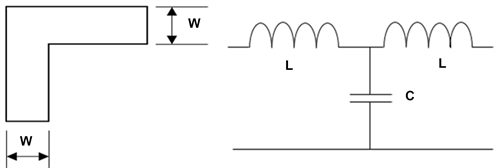
In the right-angled corner, the capacitance value increases and the area around the microstrip line will be charged; it will effectively act as a capacitance. Due to charge accumulation, particularly at the outer corner of a bend, an excess capacitance is created, while current interruptions rise because of the excessive inductances [9] . Figure 1 shows a right-angled bend and its equivalent circuit [10] .
2.3. Mitered Bends
It has been demonstrated that the mitered has a better figure of merit than unmitered in terms of the S11 (the reflected power at the transmitter) parameter at a 2.45-GHz operating frequency [11] [12] [13] . It should be considered that connecting the different elements of the Butler matrix causes the radiation of
Figure 1. Right-angled microstrip bend, Unmitered bend and its equivalent circuit.
electromagnetic waves to interface with the microstrip line and causes a loss of power in the transmission line of the Butler matrix network. In comparison, the right-angled bend provides negligible radiation loss, so that it can be used in Butler matrix systems [14] [15] .
The double-mitered case is particularly interesting, since it provides a substantially low reflection coefficient over the frequency range of 22 - 38 GHz [16] . An optimum result to connect the hybrid and patch antenna is formed by a single mitered. Therefore, the optimum mitered is computed formulas described in [14] .
To achieve better S-parameter coefficients, some parts of the microstrip line are added to the corner of a single mitered. It has been indicated that a mitered bend produces a performance at least as good as than curved bends at least up to a frequency of about 10 GHz. This applies to a wide range of bend angles, from 30˚ up to 120˚ [16] [17] .
2.4. Calculation of Initial Optimum Mitered Bend
The value of the capacitance of the optimal mitered is less than the unmitered. Therefore, the reflection coefficient is enhanced. To determine the value of h (height of substrate), the following values for different parameters are used at operating frequency of 2.4 GHz [18] :
when
when
= the effective dielectric constant of microstrip
= characteristics impedance = 50 Ω
= width of substrate
377 Ω = characteristics impedance of free space
= height of substrate = 1.44 mm
= relative permittivity
As such, the value of become 2.4 mm, and the initial value of the miter before adding substrate is 1. 99 mm. The value of will be 1.66.
3. Results
In this section, the results for the design of butler matrices are presented in two cases: 2 × 2 Butler matrix and 4 × 4 Butler matrix.
3.1. 2 × 2 Butler Matrices
To implement and design a 2-Port Butler Matrix, a hybrid coupler, two patch antennas and two micro strips transmission lines are required to connect the Hybrid and patch antenna to each other. Therefore, the optimum mitered bend in the transmission line is used to increase the S21.
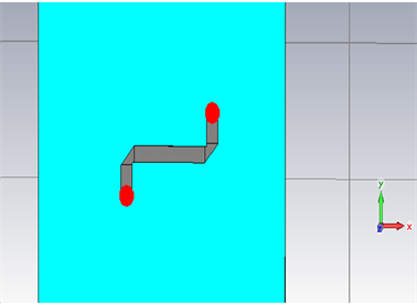
To design 90 degrees bending, the method of optimum mitered bend is utilized. Thus, the zero-phase shifter is required to connect the hybrid coupler and the patch antenna to each other, as shown in Figure 2. As the transmission line increases, the phase shifts. It indicates that the phase remains constant at 90 degrees. However, the smaller transmission line provides the better efficiency. The results show that an optimum value for S11 parameter is in length of λ/4, as shown in Figure 3. The maximum power can be transmitted or received using optimum mitered method, since the values of S12 and S21 are about zero dB at the operated frequency 2.4 GHz (see Figure 3).
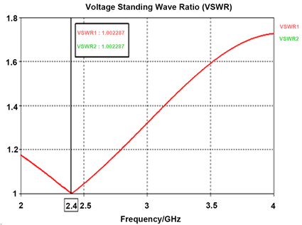
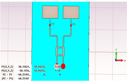
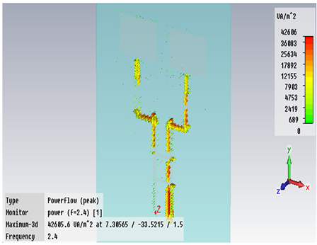
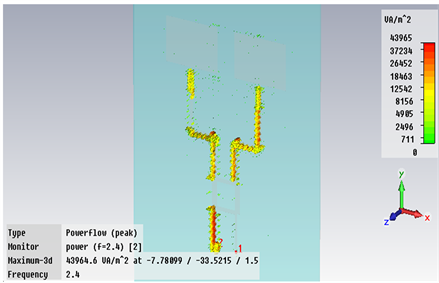
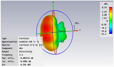
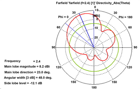
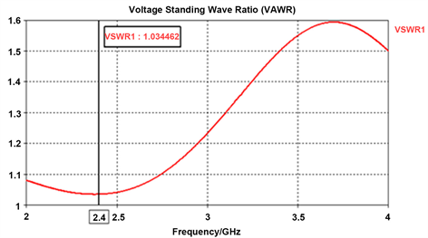
The Voltage standing wave ratio (VSWR) of the connection line between the Hybrid and the patch antenna is shown in Figure 4, which is the ratio of maximum voltage to minimum voltage that can be determined by reflection coefficient. The network system of a 2 × 2 Butler matrix feed topology, its power flow in Port 1 and Port 2 are shown in Figures 5-7, respectively. Moreover, the beam patterns of 2 × 2 Butler matrix when the Port 1 and Port 2 are connected to the source are shown in Figure 8 and Figure 9, respectively.
As it can be seen in Figure 4, the VSWR is about 1 at 2.4 GHz which demonstrates the optimum ratio of the maximum voltage to minimum voltage is achieved.
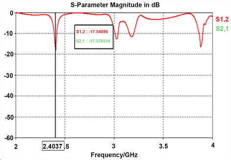
The S parameter magnitude and VSWR at the design frequency of 2 × 2 Butler matrix are shown in Figure 10 and Figure 11, respectively.
Figure 2. Connection line between Hybrid and patch antenna.
Figure 3. S parameter of connection line between Hybrid and patch antenna.
Figure 4. VSWR of the connection line between hybrid and patch antenna.
Figure 5. The 2 × 2 Butler matrices feed topology.
Figure 6. Power flow in Port 1 of 2 × 2 Butler matrix.
Figure 7. Power flow in Port 2 of 2 × 2 Butler matrix.
Figure 8. The Beam pattern of 2 × 2 Butler matrices when port 1 is fed to the source.
Figure 9. The Beam pattern of 2 × 2 Butler matrices when port 2 is fed to the source.
Figure 10. S parameter of 2 × 2 Butler matrices.
Figure 11. VSWR of 2 × 2 Butler matrices.
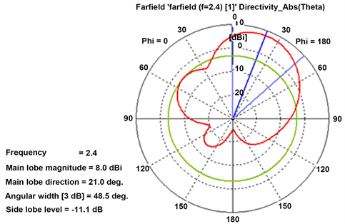
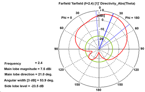
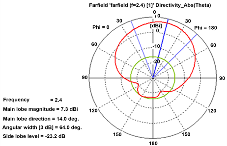
The Beam radiations of 2 × 2 Butler matrices when Port 1 and Port 2 are fed to the source by designed frequency of 2.4 GHz are shown in Figure 12 and Figure 13, respectively. Using optimum mitered method in 2 × 2 Butler matrix, the optimum power of 8 dBi magnitude at 21 main lobe direction when port 1 is fed to source is obtained (see Figure 12). More examples of the power of the main lobe magnitude when the distance between two antennas is changed are shown in Figures 14-17.
Figure 14 shows the beam direction of the first port. As distances between antennas decreased (52 mm), the S11 parameter increases by −6 dB and S12 (the power transferred from Port 2 to Port 1) or S21 (the power transferred from Port 1 to Port 2) decreases by −19 dB. Figure 15 indicates the beam direction of the second port.
Figure 16 demonstrates the beam direction of Port 1 when distances between antenna decreases (50 mm), the S11 parameter increases by −5 dB and S21 decreases by −30 dB. Figure 17 indicates the beam direction of Port 2.
3.2. 4 × 4 Butler Matrices
The 4-Port Butler Matrix provides four different phases with equivalent distances between each antenna by λ/2. Various combinations of ports can provide other beam locations and shapes. To design a 4 × 4 butler matrix, two 45 phase shifters, two crossovers, and four hybrids are required.
To determine the phase difference of the beam direction between antennas, the angles are set to:
Where is the difference phase along antennas and . The corresponding is . The values of 1R, 2L, 2R, and 1L are shown in Table 1.
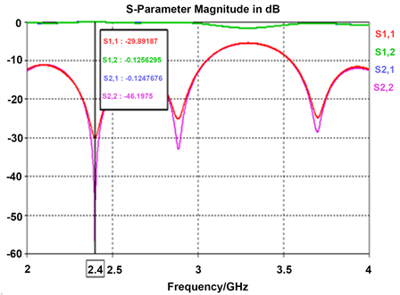
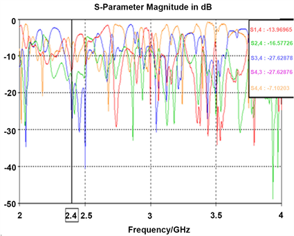
To design 4 × 4 Butler matrices, a connection between the hybrid coupler and cross over with a zero-phase shifter with optimum power is required. Consequently, the phase shifter plays an important role in this case, and a double miter is used to get an optimum result for the S parameter, as shown in Figures 18-31. The maximum power can be transmitted or received using optimum mitered method of 4 × 4 Butler matrices, since the values of S12 and S21 are about zero dB at the operated frequency 2.4 GHz (see Figure 19). The VSWR is a measure of how efficiently radio-frequency power is transmitted from a power source, through a transmission line, into a load. This value is about 1 which shows an efficient power will be transmitted through the transmission line (see Figure 21).
The optimum mitered technique used for 45 degrees phase shifter connection line between two Hybrids of 4 × 4 Butler matrix (see Figure 28). The values of S12 and S21 are about zero dB at the operated frequency 2.4 GHz (see Figure 29).
As shown in the results, isolation between adjacent beams is provided and different phase of radiation pattern are evaluated. Also, the narrow horizontal beam width capability is also achieved.
Figure 12. Beam radiation of 2 × 2 Butler matrices when port 1 is fed to source.
Figure 13. Beam radiation of 2 × 2 Butler matrices when port 2 is fed to source.
Figure 14. Beam direction of port 1 when distance between antennas decreased by 52 mm.
Figure 15. Beam direction of port 2 when distance between antennas decreased by 52 mm.
Figure 16. Beam direction of port 1 when distances between antenna decreased by 50 mm.
Figure 17. Beam direction of port 2 when distances between antenna decreased by 50 mm.
Table 1. Different phase’s element and phase radiation of beam pattern.
Figure 18. Connection line between Hybrid and cross over for 90 degrees bend.
Figure 19. S parameter of connection between Hybrid and cross over for 90 degrees bend.
4. Conclusion
This paper aims to optimize the bending area and to minimize power losses in Butler matrix network. In order to get an optimum power, the efficiency of power at the 90-degree bend in case enhances both the reflection and transmission coefficients. Therefore, a planar design, including the simulation and implementation of a transmission line with a 90-degree bend, 45 degrees phase shifter, zero phase shifter connection between patch, a hybrid coupler and a cross-over using a microstrip antenna array with Butler beam forming network
Figure 20. S parameter phase degree of connection between Hybrid and cross over for 90 degrees bend.
Figure 21. VSWR of connection between Hybrid and cross over for 90 degrees bend.
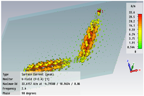
Figure 22. Surface current of connection between Hybrid and cross over for 90 degrees bend.
Figure 23. Power flow connection between Hybrid and cross over for 90 degrees bend.
Figure 24. Electric field of connection between Hybrid and cross over for 90 degrees bend.
Figure 25. Magnetic field of connection between Hybrid and cross over for 90 degrees bend.
Figure 26. Electric energy density of connection between Hybrid and cross over for 90 degrees bend.
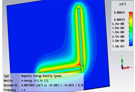
Figure 27. Magnetic energy density of connection between Hybrid and cross over for 90 degrees bend.
Figure 28. 45 degrees phase shifter connection line between two Hybrids.
Figure 29. S parameter of 45 degrees phase shifter.
Figure 30. 4 × 4 Butler matrix.
Figure 31. S parameters of 4 × 4 Butler matrices.
for wireless applications is presented for operation at 2.45 GHz. A linear antenna array is designed using the Computer Simulation Technology (CST) software. The beamforming feeder network is designed using an N × N Butler matrix, and realized using quadrature hybrids, phase shifters and crossover circuits. For simulation procedures, the main elements such as the patch antenna, hybrid, and cross-over are designed. Finally, the Butler matrix feed network is simulated and optimized to achieve the required parameters at 2.4 GHz.
Conflicts of Interest
The authors declare no conflicts of interest regarding the publication of this paper.
Cite this paper
Kiehbadroudinezhad, S., Bousquet, J.-F., Cada, M., Shahabi, A. and Kiehbadroudinezhad, M.A. (2019) Analysis and Design of Different Methods to Reach Optimum Power in Butler Matrix. Int. J. Communications, Network and System Sciences, 12, 19-35. https://doi.org/10.4236/ijcns.2019.122003
References
- 1. Kshirsagar, A.N. and Malge, P.S. (2014) Planer Implementation of Switched Beam Antenna Using Butler Matrix Feed Network. International Journal of Pure and Applied Research in Engineering and Technology, 3, 93-103.
- 2. Shiann, S.J., Garret, T.O., Guanghan, X., Hsin, P.L. and Wolfhard, J.V. (1998) Experimental Evaluation of Smart Antenna System Performance for Wireless Communications. IEEE Transactions on Antennas and Propagation, 46, No. 6.
- 3. Phan, N.T. and Gye, L. (2005) Microstrip Antenna Array with BFN for WLAN. A & P Society Symposium, Washington DC, 3-8 July 2005, 299-302.
- 4. Chu, S.H. and Lin, H.P. (2005) Performance Enhancement by Using Switched Beam Smart Antenna. Wireless Communications and Applied Computational EM Conference, Honolulu, HI, 3-7 April 2005, 1001-1005.
- 5. Vijaykumar, S.K. and Bhagwandas, A.R. (2016) Optimum Design of 4 × 4 Symmetrically Structured Butler Matrix. International Journal of Scientific Research Engineering & Technology, 5, 31-34.
- 6. El-Tager, A.M. and Eleiwa, M.A. (2009) Design and Implementation of a Smart Antenna Using Butler Matrix for ISM-Band. Progress in Electromagnetics Research Symposium (PIERS), Beijing, 23-27 March 2009, 571-575.
- 7. Kaifas, T.N. and Sahalos, J.N. (2006) On the Design of a Single Layer Wideband Butler Matrix for Switched-Beam UMTS System Applications. IEEE Antennas and Propagation Magazine, 46, No. 6.
- 8. Inder, B. and Prakash, B. (2003) Microwave Solid State Circuit Design. 2nd Edition, John Wiley & Sons, New Jersey.
- 9. Edwards, T.C. (1981) Foundations of Microstrip Circuit Design. John Wiley & Sons, Chichester, UK.
- 10. Kirschning, M., Jansen, R.H. and Koster, N.H.L. (1983) Measurement and Computer-Aided Modeling of Microstrip Discontinuities by an Improved Resonator Method. IEEE MTT-S International Symposium Digest, Boston, MA, 31 May-3 June 1983, 495-497. https://doi.org/10.1109/MWSYM.1983.1130959
- 11. Visser, H.J. (2007) Equivalent Length Design Equations for Right-Angled Microstrip Bends. The Second European Conference on Antennas and Propagation, EuCAP 2007, Edinburgh, UK, 11-16 November 2007, 1-6. https://doi.org/10.1049/ic.2007.1367
- 12. Hong, T.S., McKinzie, W.E. and Alexopoulos, N.G. (1992) Full-Wave Spectral-Domain Analysis of Compensation of Microstrip Discontinuities Using Triangular Subdomain Functions. IEEE Transactions on Microwave Theory and Techniques, 40, 2137-2147. https://doi.org/10.1109/22.179874
- 13. Rainal, A.J. (1990) Reflections from Bends in Printed Conductor. IEEE Transactions on Components, Hybrids, and Manufacturing Technology, 13, 407-413. https://doi.org/10.1109/33.56176
- 14. Douville, R.J.P. and James, D.S. (1978) Experimental Study of Symmetric Microstrip Bends and Their Compensation. IEEE Transactions on Microwave Theory and Techniques, MTT-26, 175-182. https://doi.org/10.1109/TMTT.1978.1129340
- 15. Zheng, J.X. and Chang, D.C. (1990) Numerical Modeling of Chamfered Bends and Other Microstrip Junctions of general Shape in MMIC. IEEE MTT-S International Symposium Digest, Dallas, TX, 8-10 May 1990, 709-712. https://doi.org/10.1109/MWSYM.1990.99677
- 16. Edwards, T.C. and Steer, M.B. (2000) Discontinuities in Microstrip and Stripline. In: Foundations of Interconnect and Microstrip Design, 3rd Edition, John Wiley & Sons, Ltd., West Sussex, England. https://doi.org/10.1002/9781118894514
- 17. Anders, P. and Arndt, F. (1980) Microstrip Discontinuity Capacitances and Inductances for Double Steps, Mitered Bends with Arbitrary Angle, and Asymmetric Right-Angle Bends. IEEE Transactions on Microwave Theory and Techniques.
- 18. Chen, W. (2004) The Electrical Engineering Handbook. Elsevier Science, Saint Louis.


