Engineering
Vol.5 No.9A(2013), Article ID:36781,12 pages DOI:10.4236/eng.2013.59A001
Enabling Long-Term Operation of GaAs-Based Sensors in Aqueous Solutions
1Department of Chemical Physics, Weizmann Institute of Science, Rehovot, Israel
2Chemical Research Support, Weizmann Institute of Science, Rehovot, Israel
Email: ron.naaman@weizmann.ac.il
Copyright © 2013 Maria Tkachev et al. This is an open access article distributed under the Creative Commons Attribution License, which permits unrestricted use, distribution, and reproduction in any medium, provided the original work is properly cited.
Received March 25, 2013; revised April 25, 2013; accepted May 2, 2013
Keywords: Semiconductor; GaAs; Sensor; Protection Layer; Physiological Conditions
ABSTRACT
A coating scheme was developed for enabling the operation of a GaAs-based Molecular Controlled Semiconductor Resistor (MOCSER) under biological conditions. Usually GaAs is susceptible to etching in an aqueous environment. Several methods of protecting the semiconductor based devices were suggested previously. However, even when protected, it is very difficult to ensure the operation of a GaAs-based electronic sensor in aqua solution for long periods. We developed a new depositing scheme of (3-mercaptopropyl)-trimethoxysilane (MPTMS) on GaAs substrate consisting of two separate steps. The first involves chemisorption of a dense primary MPTMS layer on the substrate, whereas in the second, a thin MPTMS polymer layer is deposited on the already adsorbed layer, resulting in a 15 - 29 nm thick coating. We show that applying the new MPTMS deposition procedure to GaAs-based MOCSER devices allows up to 15 hours of continuous electrical measurements and stable performance of the sensing device in harsh biological environment. The new protection allows implementing GaAs technology in bioelectronics, particularly in biosensing.
1. Introduction
Recent advances in microelectronics, electrochemistry, and nanotechnology make it possible to develop semiconductor-based sensors for a wide variety of applications among the biosensors [1-4]. Biosensors typically combine biological elements with a physicochemical transducer [5]. Semiconductor devices, which are based on transistor-like structures, are ideal candidates for biosensing applications due to their low production cost, small size, and direct conversion of the sensing event to changes in electrical current. Specifically, gallium arsenide (GaAs)-based sensors have interesting properties owing to the high mobility of the charge carriers and the high sensitivity to surface potential changes [6]. Moreover, the use of GaAs makes it possible to design heterostructures with special electronic properties, such as 2D electron gas and quantum wells [7]. One of the promising platforms for biosensing is the Molecular Controlled Semiconductor Resistor (MOCSER) [6,8], based on GaAs Pseudomorphic High Electron Mobility Transistor (pHEMT), which was shown to be applicable for various sensing applications [9-12]. Due to their electronic properties, GaAs-based sensors were found to be superior to silicon-based devices in terms of sensitivity [8,13].
In general, producing a stable semiconductor surface for chemical sensing is challenging, since most semiconductors tend to oxidize under ambient conditions, some of them in a non-reproducible manner. In case of GaAs, this issue is of critical importance, since GaAs is known to have a chemically unstable surface. The chemical stability issue is especially severe in aqueous environments, where the material is continuously etched due to rapid oxide dissolution in water [14].
The need to develop a reliable method for passivating GaAs surfaces was realized long ago [15]. It is especially important for any in vivo application, in which one has to protect the GaAs surface and prevent toxic arsenic compounds from penetrating into the living system. Various surface-modification techniques were explored for this purpose [16], among the inorganic sulfide treatments [17,18], adsorption of organic thiols and sulfides [19], and deposition of thiol-based self-assembled monolayers (SAM) [20,21]. However, none of these methods results in a stable enough surface that will allow the device to be operated under physiological conditions for several hours.
Hou et al. [22] employed chemical cross-linking of (3-mercaptopropyl)-trimethoxysilane (MPTMS) after depositing MPTMS SAM on GaAs in order to improve the stability of the coating. This idea was further developed by Kirchner et al. [23] to achieve functionalization of the GaAs surface by polymerization of MPTMS in a solution sol-gel process. The resulting polymer coating protects the GaAs substrate from etching in water [23]. This method was implemented in applications using MOCSER devices [11,12]. Although coating with thin MPTMS film allows corrosion protection when immersed in water, and permits electrical measurements with GaAsbased devices up to a few hours, these devices lack longterm stability. The MPTMS polymer layer is not stable enough for prolonged electrical measurements, leading to device degradation [23]. Apparently, the degradation is caused by water penetrating through tiny pinholes in the protecting polymer layer. Probably these pinholes grow in size during device operation since it is heated by the applied current, which results in etching of the GaAs at the device-polymer interface.
In the present work, we report on a new strategy for depositing MPTMS thin film on GaAs substrates. Our aim was to improve the adhesion of the primary MPTMS layer to the substrate and to deposit a more uniform polymer layer. This was achieved by separating the procedure reported previously into two steps, i.e. the depositing of the primary layer of MPTMS and the polymerization stage. The developed method allows effective protection of GaAs-based devices under physiological conditions up to 15 hours, when the system is operated continuously, without severely affecting the sensitivity of the devices.
2. Materials and Methods
2.1. Polymer Deposition
In this section we describe the old procedure (named here “regular”) for MPTMS deposition and the new technique. A comparison between the two methods for polymer deposition is presented in Table 1.
2.1.1. Regular Procedure
The procedure for depositing a protective layer of (3- mercaptopropyl)-trimethoxysilane (MPTMS) on GaAsbased devices was reported previously [11,12,23]. According to this protocol, the GaAs substrates are first cleaned in isopropanol, acetone, and ethanol (EtOH) for 10 min each and oxidized by UV/ozone (UVOCS) for 10 min. Next, the samples are etched for 5 sec in 2% hydrofluoric acid (HF), rinsed in deionized water (DDW), etched for 30 sec in ammonium hydroxide (NH4OH 25%), and then rinsed in DDW again. After etching, the substrates are dried with nitrogen and immersed immediately in ethanol solutions of MPTMS; in previous works either 0.3 vol.% (16 mM) [11], or 0.4 vol.% (21.5 mM) [12] concentrations were used. Placing in a water bath at 50°C for 4 hours allows primary MPTMS layer adsorption with thiol binding to the substrate and with the reactive methoxy groups pointing outwards [22]. Polymerization of MPTMS is initiated by adding NH4OH 25% (3 vol.% NH4OH for 0.3 vol.%, 4 vol.% NH4OH for 0.4 vol.% MPTMS concentration). The solution is kept at 50°C for additional 16 hours; then samples are rinsed with ethanol and dried with nitrogen (Table 1, Regular Procedure).
2.1.2. New Procedure
The new procedure completely separates the two steps of the “regular procedure”, i.e. the deposition of the primary layer of MPTMS and the polymerization stage (Scheme 1).
After the GaAs substrates have been cleaned and then oxidized and etched as in regular procedure, they are immersed immediately in a solution of 0.1 vol.% (5.3 mM) MPTMS in ethanol. Next, the samples are placed in a water bath at 50°C for 8 hours for primary layer deposition. For the polymerization stage, first the MPTMS concentration is increased by adding MPTMS dissolved in EtOH to get overall either 0.3 or 0.4 vol.% concentration. Then NH4OH 25% is added to initiate the polymerization (3 vol.% NH4OH for 0.3 vol.%, 4 vol.% NH4OH for 0.4 vol.% MPTMS concentration). The samples are returned to the bath at 50°C for additional 16 hours, then rinsed with ethanol and dried with nitrogen (Table 1, New Procedure).
In order to estimate the thickness of the polymer, GaAs samples were covered with MPTMS film in pa
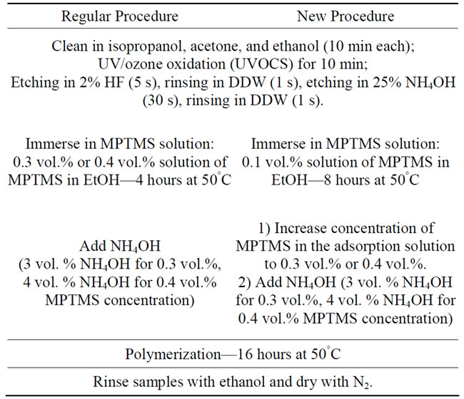
Table 1. Step-by-step MPTMS polymer deposition protocols: Regular vs New Procedures.
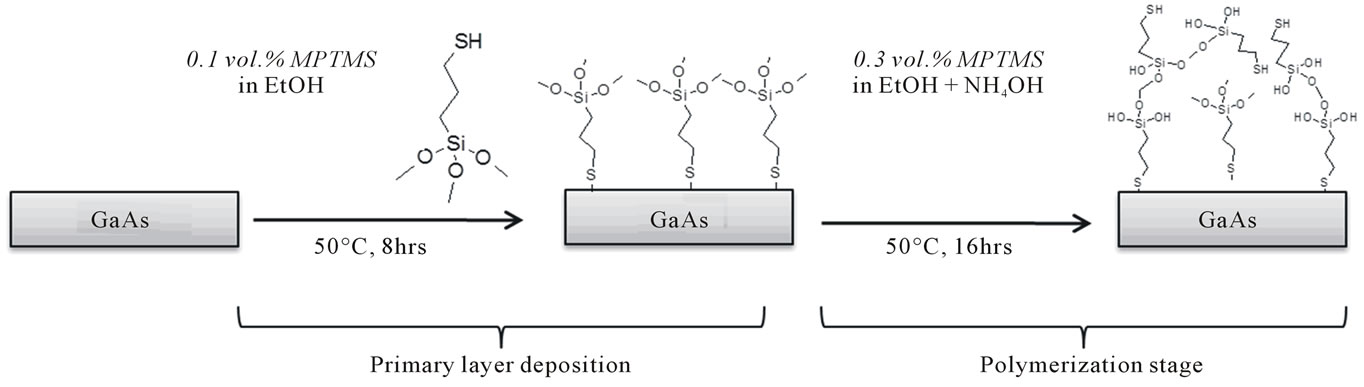
Scheme 1. Schematic representation of new procedure for MPTMS deposition. In the first stage MPTMS primary layer is adsorbed in low concentration solution, while during the polymerization stage, higher concentration of MPTMS used with added condensation agent NH4OH.
rallel with MOCSER devices and the film thickness was measured by ellipsometry (J. A. Woollam, model M- 2000V) immediately after the polymer deposition.
The quality of the primary MPTMS layer and of the MPTMS polymer layer, adsorbed on GaAs and MOCSER devices was evaluated by atomic force microscopy (see Supporting Information).
2.2. Device Fabrication and Electrical Measurements
MOCSER devices with a 600-μm long and 200-μm wide conducting channel were fabricated by standard photolithography techniques based on GaAs pHEMT wafers. Each die contained 16 devices which were measured simultaneously. In the data analysis we included only devices exhibiting normal current-voltage characteristics at the beginning of the measurement. All electrical measurements were performed on wire-bonded devices. A voltage of 1.0 V was applied and the change in sourcedrain current was monitored as a function of time (for more details see Supporting Information).
A Polydimethylsiloxane (PDMS)-based flow cell was fixed on top of the sensing area of the MOCSER. Transferring the buffer solutions to the MOCSER devices was performed at 0.03 mL/min using the peristaltic pump with teflon pipes. An Ag/AgCl reference electrode, connected via a salt bridge to the sensing chamber, was used to provide a stable reference potential in the solution (Figure S2, Supporting Information).
We used pH measurements [11] to estimate the sensitivity and stability of the polymer-coated devices. The change in the current was recorded upon exposure to phosphate buffer solutions (0.05 M) with pH 6.0, 7.0, and 8.0, for 1000 s each. Initially the measurements were performed on freshly prepared devices; then the system was left overnight to measure the baseline current at pH 7.0. The experiment was repeated after 7 - 15 hours of continuous electrical operation.
3. Results and Discussion
When an MPTMS layer is deposited by the regular procedure (see Materials and Methods), the GaAs substrate exhibits good corrosion stability when exposed to an aqueous environment for up to 24 hours [11,23]. However, continuous electrical load causes fast device degradation, expressed in reduced sensitivity and even device failure after few hours of operation. The degradation of the devices occurs apparently due to increase in temperature that leads to growing amount of defects in the MPTMS coating, penetration of water molecules to GaAs-polymer interface and subsequent etching of the surface of the device. Characterization by AFM (Figure 1) shows that after using the device at 1 V for a few hours, the polymer surface roughness (peak-to-peak and RMS values) increases relatively to freshly prepared device.
We aimed to produce thin MPTMS polymer layer strongly bound to the substrate with low-defect surface for effective long-term protection of GaAs-based devices operating in biological conditions. It was shown previously that adsorption behavior of silane coupling agents depends strongly on the solution concentration; at low concentration the molecules are adsorbed in a more regular fashion than in the case of high concentration [24]. Another important parameter is the deposition time. Thus we suggest a new strategy for forming effective protecttive film on GaAs substrates: to separate the two processes occurring in MPTMS deposition, using low concentration of the adsorption solution and increased deposition time during the primary layer formation, while regular concentrations and deposition times are used for the polymerization step. This way we allow self-organization of the adsorbed molecules on the GaAs surface during the first step, resulting in dense high-quality primary layer.
In order to establish the new coating procedure, we characterized n-doped GaAs samples and MOCSER devices with MPTMS deposited at different conditions by
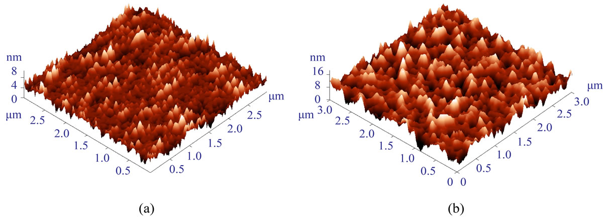
Figure 1. AFM images (3 × 3 μm) of MOCSER devices coated with MPTMS by the regular procedure (0.4 vol.% solution of MPTMS) before (a) and after (b) electrical measurements in aqueous environments for several hours. Surface roughness (peak-to-peak and RMS values) increased after the measurements. The RMS value increases from 1.43 nm to 2.58 nm (Note the difference in scale between a and b).
ellipsometry and AFM. First, we evaluated the optimal conditions for the primary layer adsorption, and then probed the surface of the polymerized MPTMS layer deposited on top of the modified primary layer.
Eventually, we conducted a series of electrical measurements on MOCSER devices in order to assess the validity of the proposed method. These sensing measurements performed on MOCSERs coated with MPTMS by regular and new procedures show ultimately that the new strategy improves dramatically stability of the GaAsbased devices in biological conditions without losing sensitivity.
3.1. Primary MPTMS Layer Characterization
For probing the influence of the adsorption conditions on the quality of the MPTMS primary layer, we prepared a set of films on GaAs; in these experiments the concentrations of MPTMS and the adsorption times were varied, and no ammonium hydroxide was added. No polymerization occurs in this case; thus only a primary layer is deposited. The AFM and ellipsometry characterization data are summarized in Table 2.
Adsorption of MPTMS on GaAs from ethanol solutions with different concentrations results in multilayer film more than 2 nm thick. This can be attributed to oligomerization of MPTMS in solution and the subsequent adsorption on the GaAs surface [25]. If the film deposited for 4 hours only, it is not evident from the AFM results that the quality of the primary layer depends on the concentration of the adsorption solution (changes in RMS values are within error range). However, we found it to depend strongly on the deposition time. For samples prepared from 0.4 vol.% MPTMS solutions, increasing the deposition time from 4 to 20 hours results in lower peak-to-peak values and decreasing of the RMS values from 0.60 to 0.39 nm. In case of 0.1 vol.% MPTMS solu
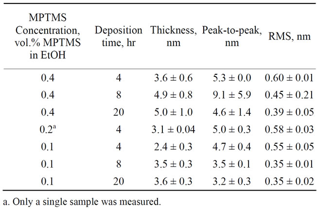
Table 2. Summary of the primary MPTMS layer adsorption experiments.
tions, RMS improves from 0.55 nm for 4 hours to 0.35 nm for 8 hours of adsorption, while further increasing of deposition time does not affect the surface smoothness (see Table 2). Moreover, in case of 8 hours deposition, decreasing concentration of adsorption solution to 0.1 vol.% MPTMS significantly improves the roughness (RMS = 0.35 nm) relatively to high concentration of 0.4 vol.% (RMS = 0.45 nm).
Thus we suggest that setting the primary layer conditions to 0.1 vol.% MPTMS and 8 hours of deposition produces a dense primary layer with better adhesion to the substrate. Moreover, it results in a more uniform polymer layer produced during the polymerization stage (see below).
3.2. Characterization of the Polymerized MPTMS layer
In this part of the work we probed how the primary layer deposition conditions affected the polymerization step. We found that solutions with low concentrations of MPTMS (0.1 and 0.2 vol.% MPTMS in EtOH) do not form a continuous polymerized layer (see Supporting Information), whereas solutions with higher concentrations of 0.3 and 0.4 vol.% of MPTMS result in a continuous polymer layer.
Therefore, we used 0.3 and 0.4 vol.% MPTMS concentrations for the polymerizatoion stage, while varying the conditions for the primary layer adsorption. This included increasing the deposition time from 4 to 8 hours and decreasing the concentration to 0.1 vol.% MPTMS during the first step. Several samples were prepared on different days and the thickness of the resulting polymer was estimated by ellipsometry. The high deviations in the MPTMS layer thickness observed (see Table 3) are attributed to variations in air humidity during sample preparation. As a consequence, comparative roughness analysis is problematic for polymer samples prepared on different days. For this reason, we compared here AFM data of samples prepared on the same day—for concentrations of 0.4 vol.% MPTMS (AFM Set #1), and for 0.3 vol.% MPTMS (AFM Set #2). Another difficulty in obtaining quantitative roughness estimation arises from the defects present on the polymer surface. To reduce errors resulting from polymer agglomerations, we performed roughness analysis on defect-free areas. Typical AFM images are shown in Figures 2 and 3; the AFM data analysis and ellipsometry characterization are summarized in Table 3.
When the polymer deposition is performed in a solution of 0.4 vol.% MPTMS, the thickness of the resulting layer ranges from 18 to 33 nm, whereas for 0.3 vol.% MPTMS the polymer thickness decreases to 15-29 nm. Changing the primary layer adsorption conditions did not affect the quality of the polymer layer with the 0.4 vol.% MPTMS concentration. In contrast, for samples prepared in a 0.3 vol.% MPTMS solution, the primary adsorbed layer profoundly affected the overall polymer quality. When the first layer is adsorbed from solutions with low concentrations and long deposition times, both peak-topeak and RMS values in the AFM images are signifycantly reduced in this case, indicating the role of the primary layer in improving the overall surface quality.
3.3. Sensing Measurements
The ultimate check for assessing the quality of the protection layer lies in the sensing measurements, which provide information on both the sensitivity and the ability of the layer to protect the devices for a long time, namely, the stability. To this end, we prepared several MOCSER devices covered with MPTMS under different conditions. On each of them a series of measurements were performed, to test their stability and sensitivity. For this purpose phosphate buffer solutions at different pHs were used. The change in the normalized current as a function of time upon exposure to solutions with pH 6, 7, and 8 is shown in Figures 4 and 5 (normalized current is calculated as (I-I0) * 103/I0, see Supporting Information). The measurements were conducted first on freshly prepared devices and then they were repeated after 7 - 15 hours of continuous operation of the device. The results of sensing experiments are summarized in Table 4.
In general, devices coated with a polymer prepared in 0.4 vol.% MPTMS solutions (cases a and b, Table 4) are significantly less stable than devices prepared in 0.3 vol.% MPTMS solutions. Some of the MOCSER devices, prepared with the 0.4 vol.% MPTMS solution, stopped working already during the initial pH measurements, and those that survived after 12 hours lost their sensitivity. In case of the modified primary layer (0.1 vol.% MPTMS for 8 hours) and the 0.4 vol.% MPTMS solution for the polymerization step (case c, Table 4), the devices are sensitive to pH changes both when fresh and after 12 hours of measurements (not shown). Moreover, the sensitivity of the devices prepared with 0.4 vol.% MPTMS solution during polymerization is lower than that observed in case of 0.3 vol.% MPTMS polymerization, apparently due to higher thickness of the protective layer.
MOCSER device prepared with a 0.3 vol.% MPTMS solution according to regular procedure (case d, Table 4) exhibited high sensitivity when fresh (Figure 4(a)), but only 6 out of 10 MOCSER channels survived the 7-hour operation and the device sensitivity significantly decreased (Figure 4(b)). After 15 hours of continuous measurements, most of the devices failed.
When the device is covered with MPTMS according to the new procedure (case e, Table 4), all 8 channels that worked at the beginning of the experiment exhibit stable performance. Interestingly, the same 8 channels were still sensitive to pH changes after 15 hours of continuous measurements. Figure 5 shows the average signal obtained from the 8 MOCSER channels upon changes in pH with a fresh MPTMS coating (a) and after 15 hours of operation (b).
Following the sensing experiments, the effect of the electrical measurements on the surface of the protecting polymer layer was probed by AFM. We characterized the surfaces of the devices prepared in 0.3 vol.% MPTMS polymerization solutions. First, a scan of 13 × 13 μm was performed followed by measuring several regions of 3 × 3 μm. The AFM data are summarized in Table 5 and presented in Figure 6.
In the case of devices prepared by the regular procedure (case d, Table 4), it is obvious that the number of surface defects increases significantly after the electrical measurements (see Figures 6(a) and (b)). Roughness analysis reveals that not only the density of defects increased but also the peak-to-peak and RMS values increased dramatically (Table 5).
When MOCSER devices are coated with MPTMS ac
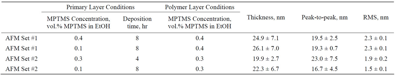
Table 3. Summary of the MPTMS polymer deposition experiments.
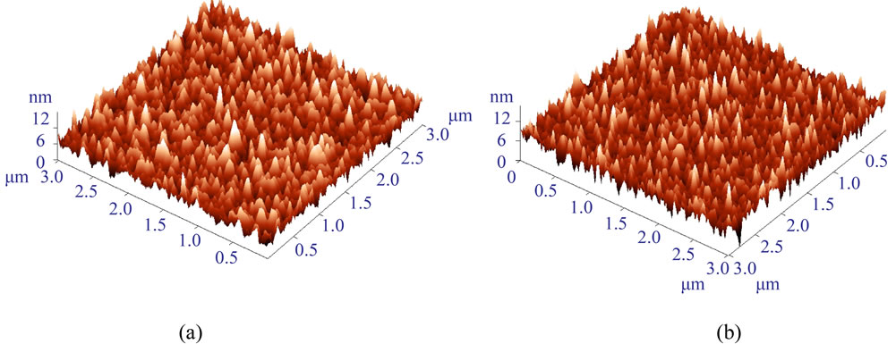
Figure 2. AFM images of GaAs samples with MPTMS polymer deposited in a solution of 0.4 vol.% MPTMS. (a) The same concentration of 0.4 vol.% MPTMS was used for the primary layer (8 hours) and for the polymer layer adsorption. (b) The primary layer deposited in 0.1 vol.% MPTMS solution for 8 hours and the polymer layer adsorbed in 0.4 vol.% MPTMS solution. No significant difference in surface roughness was observed (samples prepared on the same day).
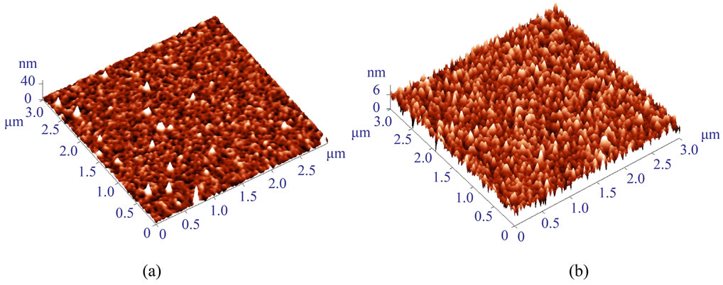
Figure 3. AFM images of GaAs samples with the MPTMS polymer deposited in a solution of 0.3 vol.% MPTMS. (a) The same concentration of 0.3 vol.% MPTMS was used for the primary layer (4 hours) and for the polymer layer adsorption (regular procedure). (b) The primary layer deposited in 0.1 vol.% MPTMS solution for 8 hours and the polymer layer adsorbed in 0.3 vol.% MPTMS solution. The roughness significantly decreases with the new procedure. There are numerous point defects in (a); here roughness analysis was performed on defect-free areas and not on the whole scan (the samples prepared on the same day).
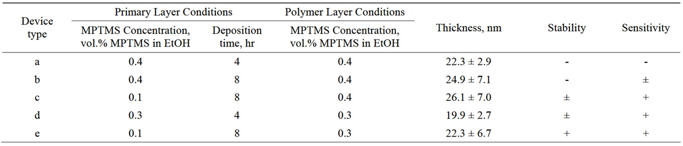
Table 4. Summary of electrical measurements.
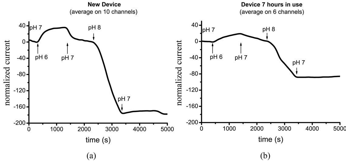
Figure 4. Responses of MOCSER devices covered with MPTMS by the regular procedure (0.3 vol.% MPTMS for both 4-hour primary layer adsorption and for the polymerization step). (a) Freshly prepared device exhibits good response on 10 channels. (b) After 7 hours of operation, 4 channels fail, and a lower response is exhibited by the remaining 6 working channels.
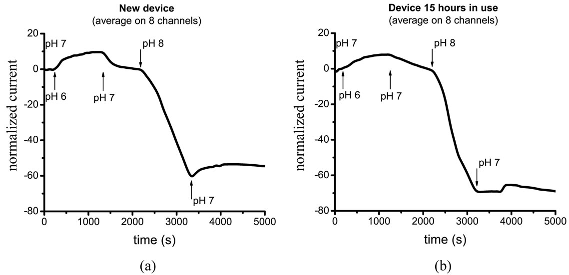
Figure 5. MOCSER response to pH changes in case of MPTMS deposited according to the new procedure (0.1 vol.% MPTMS for 8 hours of primary layer adsorption, 0.3 vol.% MPTMS for the polymerization step). (a) Freshly prepared device exhibits good performance on 8 channels. (b) The same 8 channels still working after 15 hours of operation exhibit good sensitivity to pH changes.
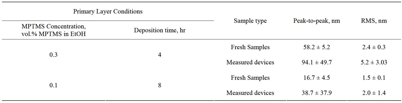
Table 5. AFM data for samples and devices prepared in 0.3 vol.% MPTMS polymerization solutions before and after electrical measurements.
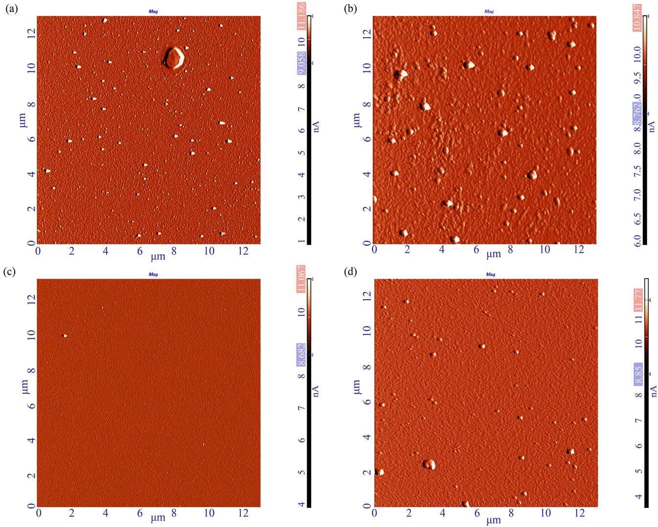
Figure 6. AFM images (amplitude images of 13 × 13 μm scan) of the polymer layer, prepared under the regular conditions with a 0.3 vol.% MPTMS solution (a, b) and with the new procedure—0.1 vol.% MPTMS solution for the primary layer deposition for 8 hours, and 0.3 vol.% MPTMS solution for the polymerization step (c, d). (a) Freshly deposited MPTMS according to the regular procedure on an n-type GaAs sample. (b) MOCSER device surface covered according to the regular procedure after electrical measurements of the device for 15 hours. The density of the polymer irregularities increased after the device was operated under electrical stress in an aqueous environment. (c) Freshly deposited MPTMS according to the new procedure on an n-type GaAs sample. A very low density of surface irregularities was observed. (d) The MOCSER device surface covered according to the new procedure after taking electrical measurements of the device. The number of polymer irregularities increased after the device was operated for 15 hours, but the overall density of these defects is much lower than in (b) and is comparable to that of the device freshly prepared by regular procedure (a).
cording to the new procedure (adsorption of primary layer in 0.1 vol.% MPTMS solution for 8 hours, and 0.3 vol.% MPTMS solution for polymerization—case e, Table 4), a significantly lower number of surface defects is observed on an MPTMS-covered surface of the fresh samples (Figure 6(c)). Although the number of defects increases after electrical test in this case, the number of surface defects is still much lower than that observed for devices coated by the regular procedure (Figure 6(d)). Moreover, increase in surface roughness during the device operation is much less significant than in the case of regular MPTMS deposition: peak-to-peak and RMS values of the operated device are comparable to those of fresh device prepared by the old method (see Table 5, compare Figures 6(a) and (d)).
4. Conclusion
In this work we present a simple and effective procedure for long-term protection of GaAs-based devices, operating under biological conditions, with thin polymer layer of MPTMS. In contrast to procedure suggested and implemented before [11,12,23], the new method ensures more uniform and stable primary layer deposition covalently bound to the GaAs substrate, which results in better adhesion and lower amount of defects on the surface of the MPTMS polymer layer. While devices coated with MPTMS by regular procedure usually fail after few hours of operation, the new method allows continuous electrical measurements of GaAs-based devices in aqueous environments for more than 15 hours without losing sensitivity. We argue that achieved high-quality primary layer with better surface quality of the polymer decreases the number of pinholes in MPTMS layer and thus prevents penetrating of water molecules from the solution to GaAs-MPTMS interface with subsequent etching of the device surface, which causes device malfunction. In addition, the new procedure makes it possible to operate MOCSER-based sensor in aqueous environments even at very low pHs (data not shown). Thus applying the new procedure for MPTMS deposition presented in this work, allows long-term protection and stable performance of GaAs-based devices in physiological conditions, which is essential for further development of GaAs technology in the fast-growing field of biosensors and bioelectronics.
5. Acknowledgements
Partial support from the Grand Center for Sensors and Security is acknowledged.
REFERENCES
- F. J. Arregui, “Sensors Based on Nanostructured Materials,” Springer, New York, 2009. doi:10.1007/978-0-387-77753-5
- M. S. Makowski and A. Ivanisevic, “Molecular Analysis of Blood with Micro-/Nanoscale Field-Effect-Transistor Biosensors,” Small, Vol. 7, No. 14, 2011, pp. 1863-1875. doi:10.1002/smll.201100211
- A. B. Dahlin, B. Dielacher, P. Rajendran, K. Sugihara, T. Sannomiya, M. Zenobi-Wong and J. Vörös, “Electrochemical Plasmonic Sensors,” Analytical and Bioanalytical Chemistry, Vol. 402, No. 5, 2012, pp. 1773-1784. doi:10.1007/s00216-011-5404-6
- T. Aqua, R. Naaman, A. Aharoni, U. Banin and Y. Paltiel, “Hybrid Nanocrystals-Organic-Semiconductor Light Sensor,” Applied Physics Letters, Vol. 92, No. 2, 2008, Article ID: 223112. doi:10.1063/1.2940230
- D. R. Thévenot, K. Toth, R. A. Durst and G. S. Wilson, “Electrochemical Biosensors: Recommended Definitions and Classification,” Biosensors and Bioelectronics, Vol. 16, No. 1-2, 2001, pp. 121-131. doi:10.1016/S0956-5663(01)00115-4
- K. Gartsman, D. Cahen, A. Kadyshevitch, J. Libman, T. Moav, R. Naaman, A. Shanzer, V. Umansky and A. Vilan, “Molecular Control of a GaAs Transistor,” Chemical Physics Letters, Vol. 283, No. 5-6, 1998, pp. 301-306. doi:10.1016/S0009-2614(97)01387-0
- D. Delagebeaudeuf, P. Delescluse, P. Etienne, M. Laviron, J. Chaplart and N.T. Linh, “Two-Dimensional Electron Gas m.e.s.f.e.t. Structure,” Electronics Letters, Vol. 16, No. 17, 1980, pp. 667-668. doi:10.1049/el:19800473
- E. Capua, A. Natan, L. Kronik and R. Naaman, “The Molecularly Controlled Semiconductor Resistor: How does it work?” ACS Applied Materials & Interfaces, Vol. 1, No. 11, 2009, pp. 2679-2683. doi:10.1021/am9005622
- M. R. Vilar, J. El-Beghdadi, F. Debontridder, R. Naaman, A. Arbel, A. M. Ferraria and A. M. B. Do Rego, “Development of Nitric Oxide Sensor for Asthma Attack Prevention,” Materials Science and Engineering, Vol. 26, No. 2-3, 2006, pp. 253-259. doi:10.1016/j.msec.2005.10.064
- E. Capua, R. Cao, C. N. Sukenik and R. Naaman, “Detection of Triacetone Triperoxide (TATP) with an Array of Sensors Based on Non-Specific Interactions,” Sensors and Actuators B: Chemical, Vol. 140, No. 1, 2009, pp. 122-127. doi:10.1016/j.snb.2009.04.045
- D. Bavli, M. Tkachev, H. Piwonski, E. Capua, I. de Albuquerque, D. Bensimon, G. Haran and R. Naaman, “Detection and Quantification through a Lipid Membrane Using the Molecularly Controlled Semiconductor Resistor,” Langmuir, Vol. 28, No. 1, 2012, pp. 1020-1028. doi:10.1021/la203502b
- A. K. Tatikonda, M. Tkachev and R. Naaman, “A Highly Sensitive Hybrid Organic-Inorganic Sensor for Continuous Monitoring of Hemoglobin,” Biosensors and Bioelectronics, Vol. 45, 2013, pp. 201-205. doi:10.1016/j.bios.2013.01.040
- R. Naaman, “Molecular Controlled Nano-Devices,” Physical Chemistry Chemical Physics, Vol. 13, No. 29, 2011, pp. 13153-13161. doi:10.1039/c1cp21106d
- M. R. Vilar, J. El Beghdadi, F. Debontridder, R. Artzi, R. Naaman, A. M. Ferraria and A. M. B. Do Rego, “Characterization of Wet-Etched GaAs (100) Surfaces,” Surface and Interface Analysis, Vol. 37, No. 8, 2005, pp. 673-682. doi:10.1002/sia.2062
- A. M. Green and W. E. Spicer, “Do We Need a New Methodology for GaAs Passivation?” Journal of Vacuum Science & Technology A, Vol. 11, No. 4, 1993, pp. 1061- 1069. doi:10.1116/1.578442
- F. Seker, K. Meeker, T. F. Kuech and A. B. Ellis, “Surface Chemistry of Prototypical Bulk II-VI and III-V Semiconductors and Implications for Chemical Sensing,” Chemical Reviews, Vol. 100, No. 7, 2000, pp. 2505-2536. doi:10.1021/cr980093r
- V. N. Bessolov, M. V. Lebedev, A. F. Ivankov, W. Bauhofer and D. R. T. Zahn, “Electronic Properties of GaAs(100) Surface Passivated in Alcoholic Sulfide Solutions,” Applied Surface Science, Vol. 133, No. 1-2, 1998, pp. 17-22. doi:10.1016/S0169-4332(98)00189-5
- E. V. Konenkova, “Modification of GaAs(100) and GaN(0001) surfaces by treatment in alcoholic sulfide solutions,” Vacuum, Vol. 67, No. 1, 2002, pp. 43-52. doi:10.1016/S0042-207X(02)00199-9
- S. R. Lunt, G. N. Ryba, P. G. Santangelo and N. S. Lewis, “Chemical Studies of the Passivation of GaAs Surface Recombination Using Sulfides and Thiols,” Journal of Applied Physics, Vol. 70, No. 12, 1991, pp. 7449-7467. doi:10.1063/1.349741
- X. Ding and J. J. Dubowski, “Surface Passivation of (001) GaAs with Self-Assembled monolayers of Long-Chain Thiols,” Proceedings of the SPIE, Vol. 5713, 2005, pp. 545-551. doi:10.1117/12.605649
- P. Arudra, G. M. Marshall, N. Liu, and J. J. Dubowski, “Enhanced Photonic Stability of GaAs in Aqueous Electrolyte Using Alkanethiol Self-Assembled Monolayers and Postprocessing with Ammonium Sulfide,” The Journal of Physical Chemistry C, 2012, Vol. 116, No. 4, pp. 2891-2895. doi:10.1021/jp208604v
- T. Hou, C. M. Greenlief, S. W. Keller, L. Nelen and J. F. Kauffman, “Passivation of GaAs (100) with an Adhesion Promoting Self-Assembled Monolayer,” Chemistry of Materials, Vol. 9, No. 12, 1997, pp. 3181-3186. doi:10.1021/cm9704995
- C. Kirchner, M. George, B. Stein, W. J. Parak, H. E. Gaub and M. Seitz, “Corrosion Protection and LongTerm Chemical Functionalization of Gallium Arsenide in an Aqueous Environment,” Advanced Functional Materials, Vol. 12, No. 4, 2002, pp. 266-276. doi:10.1002/1616-3028(20020418)12:4<266::AID-ADFM266>3.0.CO;2-U
- N. Nishiyama, K. Horie and T. Asakura, “Adsorption Behavior of a Silane Coupling Agent onto a Colloidal Silica Surface Studied by 29Si NMR Spectroscopy,” Journal of Colloid and Interface Science, Vol. 129, No. 1, 1989, pp. 113-119. doi:10.1016/0021-9797(89)90420-7
- Gelest, Inc., “Silane Coupling Agents: Connecting Across Boundaries,” 2003. http://www.gelest.com/goods/pdf/couplingagents.pdf
1. Supporting Information
1.1. Materials
3-Mercaptopropyl trimethoxysilane (MPTMS) was purchased from Sigma. Sodium phosphate monobasic (Cat. No. 567545) and sodium phosphate dibasic (Cat. No. 567550) were obtained from Merck KGaA, Darmstadt, Germany. Polydimethylsiloxane (PDMS) was purchased from DowCorning Inc. Med-1000 silicon adhesive was obtained from NuSil Silicon Technology. Deionized Milli Q water (DDW) was used for the buffer preparation and experiments. GaAs Pseudomorphic High Electron Mobility Transistor (pHEMT) wafers for MOCSER devices fabrication were supplied by IQE Inc.
1.2. AFM Imaging
The quality of the primary MPTMS layer and of the MPTMS polymer layer, adsorbed on GaAs and MOCSER devices was evaluated by atomic force microscopy (AFM). The topography images of MPTMS coatings on GaAs were acquired using atomic force microscope P47 (NT-MDT, Zelenograd) equipped with small scanner.
Images were recorded in the tapping mode in the air at the room temperature 22˚C - 24˚C using silicon micro cantilevers (OMCL-AC240TS-W2, Olympus) with nominal spring constant 2 N/m and resonant frequency 70 kHz (manufacturer specified). The set point ratio was adjusted to 0.75 - 0.8 (corresponding to the “light” tapping) and the scan rate was set to 1 Hz. Imaging has been carried out at the different scales (13 × 13, 5 × 5 and 3 × 3 mm) to verify the consistency and robustness of the evaluated structures. Image analysis was performed using Nova 1.0.26.1443 software.
The AFM characterization of the obtained MPTMS layers was performed both on n-doped GaAs substrates and on MOCSER devices. In order to verify that the MPTMS polymer prepared on the devices is similar to polymer adsorbed on the GaAs substrates, we coated MOCSER devices and GaAs-based samples with MPTMS at the same conditions and characterized the surfaces with AFM. Indeed, the polymer layers adsorbed under the same conditions on GaAs and MOCSER devices produce similar AFM data (Figure S1).
There are always surface defects present which look
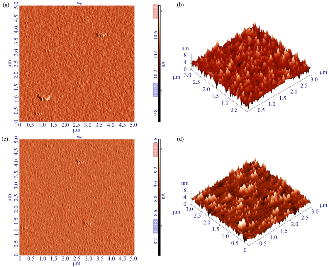
Figure S1. AFM images of polymer layer, prepared at the regular conditions with 0.4 vol.% MPTMS in EtOH solution on n-type GaAs sample (a,b) and GaAs pHEMT-based MOCSER device (c,d). (a, c) Amplitude images of 5 × 5 μm scans show similar polymer agglomerating sites both on MOCSER and GaAs substrates. (b, d) 3 × 3 μm scans of defect-free areas where the roughness analysis was performed.
like polymer agglomerations on top of the polymer layer (Figure S1(a) and (c)). In order to estimate the overall surface quality, large areas of 13 × 13 or 5 × 5 μm were scanned. For quantitative surface roughness analysis we chose defect-free regions, so that several regions of 3 × 3 μm were analyzed for each sample.
1.3. Device Fabrication, Electrical Measurements, and Data Analysis
MOCSER devices with a 600 μm long and 200 μm wide conducting channel were fabricated by standard photolithography techniques based on GaAs Pseudomorphic High Electron Mobility Transistor structure. Each die contained 16 devices, which were measured simultaneously. All the electrical measurements were performed on wire-bonded devices using two Keithley 236 sourcemeasure units. The system was controlled and monitored by Labview application (version 8.6). A voltage of 1.0 V was applied between source and drain of the MOCSER devices and the change in source-drain current was monitored as a function of time.
Polydimethylsiloxane (PDMS)-based flow cell (4 mm in length and width and 0.6 mm in height) was fixed on top of the sensing area of the MOCSER with MED-1000 silicon adhesive. Transferring of buffer solutions to the MOCSER devices was performed at 0.03 mL/min using the peristaltic pump (EP-1 Econo pump, Bio-Rad Laboratories Israel) with teflon pipes (inner diameter of 0.8 mm). Ag/AgCl reference electrode connected via a salt bridge to sensing chamber was used to provide a stable reference potential in the solution (Figure S2).
In the data analysis we included only devices exhibiting normal current-voltage characteristics at the beginning of the measurement. The measured current on each MOCSER was normalized as follows: I = (I-I0) * 103/I0, where I0 is the baseline current with pH 7, before introducing buffer with pH 6. In addition, in order to remove the influence of current drift with time, the baseline correction was performed according to baseline current with pH 7, and the average signal on the working devices was calculated.
1.4. Additional Results
While trying to evaluate optimal conditions for polymerization, we found that solutions with low concentrations of the MPTMS (0.1 and 0.2 vol.% MPTMS in EtOH) do not allow formation of a continuous polymerized layer. The structures look like continuous primary layer with circular polymer agglomerations on top of it (Figure S3).
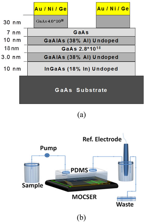
Figure S2. (a) Schematic representation of the GaAs Pseudomorphic High Electron Mobility Transistor (pHEMT) structure used for MOCSER device fabrication. (b) Schematic representation of the experimental setup. A peristaltic pump was used to transfer analyte samples to MOCSER sensing area inside PDMS-based flow cell. An Ag/AgCl reference electrode was connected via a salt bridge.
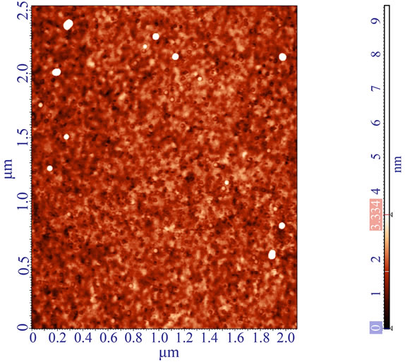
Figure S3. AFM image of non-continuous layer obtained when polymerization occurs at low concentration 0.1 vol.% MPTMS in EtOH