Intelligent Control and Automation
Vol.5 No.1(2014), Article ID:43063,11 pages DOI:10.4236/ica.2014.51001
Power Factor Correction Rectifier with a Variable Frequency Voltage Source in Vehicular Application
Electric Vehicle and Power Electronics Group (VEEP), Laboratory of Electronics and Information Technology (LETI), National School of Engineers of Sfax (ENIS), University of Sfax, Sfax, Tunisia
Email: amine_toumi_tn@yahoo.fr, radhouan.mail@gmail.com, moez.ghariani@isecs.rnu.tn, moez.ayadi@enis.rnu.tn, rafik.neji@enis.rnu.tn
Copyright © 2014 Amine Toumi et al. This is an open access article distributed under the Creative Commons Attribution License, which permits unrestricted use, distribution, and reproduction in any medium, provided the original work is properly cited. In accordance of the Creative Commons Attribution License all Copyrights © 2014 are reserved for SCIRP and the owner of the intellectual property Amine Toumi et al. All Copyright © 2014 are guarded by law and by SCIRP as a guardian.
Received October 6, 2013; revised November 6, 2013; accepted November 13, 2013
KEYWORDS: Asynchronous Machine; Control-Oriented Vector of Rotor Flux; PWM; Boost Converter; Harmonic Injection; Power Factor Correction; Three-Phase Rectifier; Junction Temperature
ABSTRACT
This paper presents a PFCVF (Power Factor Correction) rectifier that uses a variable frequency source for alternators for electric and hybrid vehicles application. In such application, the frequency of the signal in the alternator changes according to the vehicle speed, more over the loading effect on the alternator introduces harmonic currents and increases the alternator apparent power requirements. To overcome these problems and aiming more stability and better design of the alternator, a new third harmonic injection technique is proposed. This technique allows to preserve a good THD (Total Harmonic Distortion) of the input source at any frequency and to decrease losses in semiconductors switches, thereby allowing more stability and reducing the apparent power requirements. A comparative study between the standard and the new technique is made and highlights the effectiveness of the new design. A detailed analysis of the proposed topology is presented and simulations as well as experimental results are shown.
1. Introduction
This technology has more than three decades of sustained technological and theoretical development. It can be fulfilled that these high-performance rectifiers conform to modern standards and have been widely accepted in industry. The simplest line-commutated converters use diodes to transform the electrical energy from AC to DC. The major disadvantage of these commutated converters is the reactive power and the generation of harmonics [1-3]. Harmonics have a negative consequence on electrical systems operation; so, increasing attention is paid to their generation and control [4,5]. One of the most popular PFC (Power Factor Correction) methods for three-phase input is a full-bridge type pulse with modulation (PWM) rectifier. The conventional PWM rectifier allows obtaining a sinusoidal input current without harmonics distortion. However, in regard to cost, the conventional PWM rectifier is not the best solution for the PFC [6-9]. One basic method to reduce input current harmonics is the use of multi-pulse connections based on transformers with multiple windings. An extra improvement is the use of passive power filters. In the last years, active filters were introduced to reduce the harmonics injected to the mains supply. An additional way of harmonics diminution is the power-factor correction (PFC). Within these converters, controlled power switches like gate-turn-off thyristors (GTOs), insulated gate bipolar transistors (IGBTs), are integrated in the rectifier power circuit to change actively the input current waveform, reducing the distortion [10]. These circuits reduce harmonics and improve the power factor.
Harmonic currents cause additional Joule losses in conductors. Their presence reduces the lifetime of the alternators and increases their apparent power requirements.
In this paper, we present a Power Factor Correction rectifier (PFCVF) that uses a variable frequency source for alternators for electric and hybrid vehicles application. This solution aims to improve stability, minimize losses and reduce alternator apparent power requirements for the sake of a better design, better performance and lower cost. Firstly, we present the synchronous alternator model. In the second section, we describe the third harmonic injection method. As we use a tuned circuit in this injection method, a fixed frequency current injection is applied which is useful only at a fixed frequency source. A new part in the injection method is presented. It generates a sine wave current for injection and can modify the amplitude, the frequency and even the form of the injected signal. The new designed circuit works at a large frequency range of the input source. In the third section, thermal modeling of the power module is proposed. Finally, simulations and experimental results are detailed to highlight the effectiveness of the new design.
2. Synchronous Alternator Description
The used machine, is synchronous [11,12] with salient poles; its model is shown in figure 1.
The dynamic model of this machine can be described as follows:
 (1)
(1)
 (2)
(2)
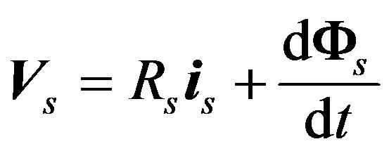
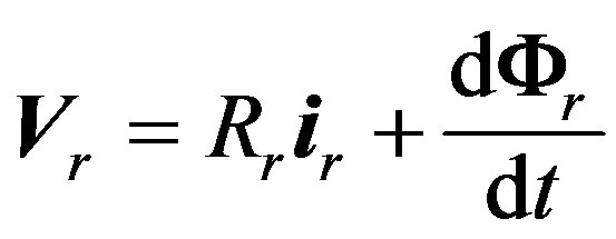
where:  is the stator voltage vector, and
  the rotor voltage one.
2.1. Voltage Equations
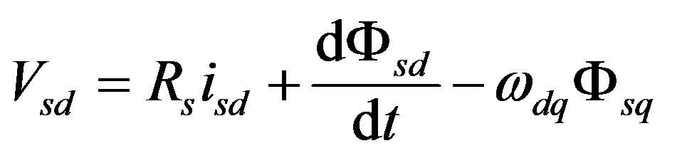
The rotor iron losses are neglected (the rotor frequencies are very weak compared to the stator frequencies). The voltage equations, according to Park model, in the stator frame are given by the following equations:
 (3)
(3)
 (4)
(4)
 (5)
(5)
2.2. Current Equation
The current equation in stator frame is given by the following equation:
 (6)
(6)

Figure 1. Machine model.
2.3. Flux Equations
 (7)
(7)
 (8)
(8)
 (9)
(9)
 (10)
(10)
3. Third Harmonic Current Injection
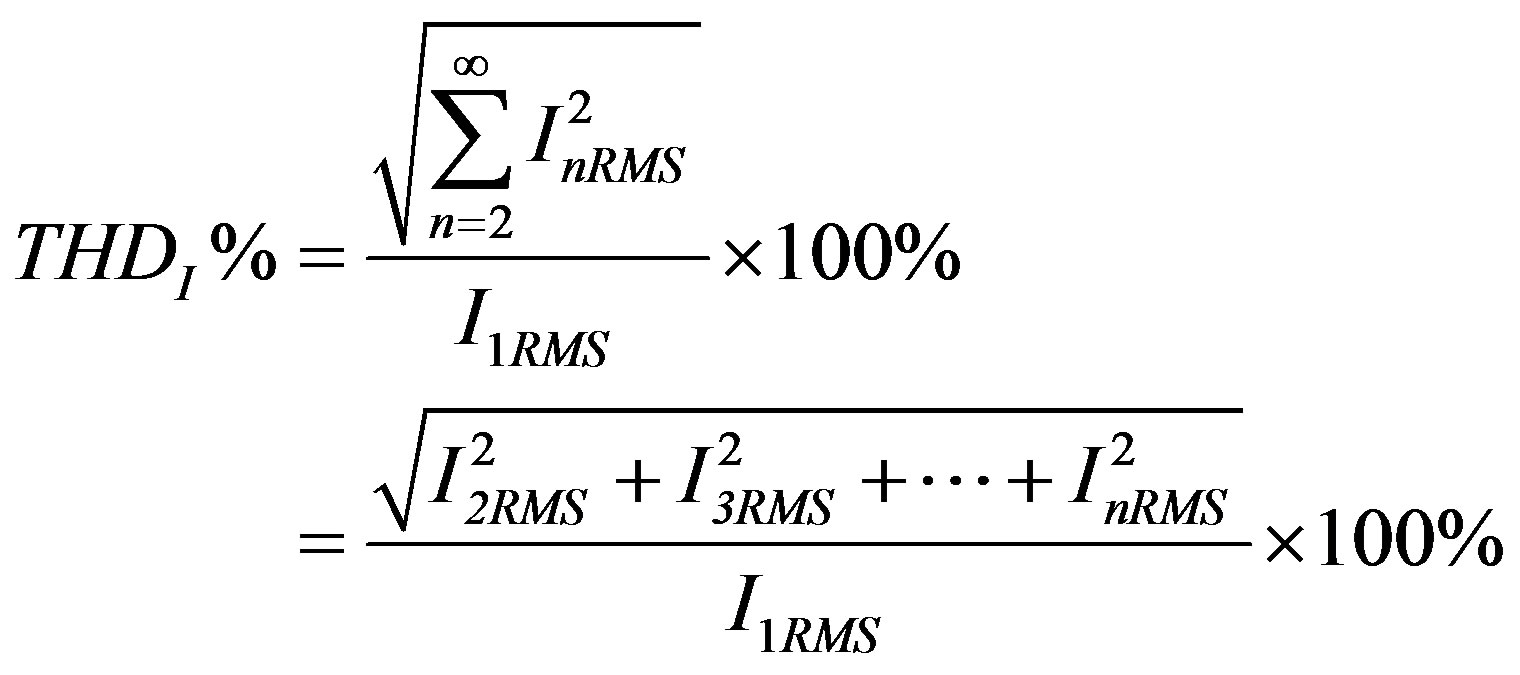
Since one phase voltage cannot be the highest and the lowest at the same time for the given set of phase voltages, two of the phases are connected to the load while one phase is unconnected in each point. This results in an input current equal to zero in the time interval when the phase voltage is neither maximal nor minimal. The gaps in the phase currents are the main reason for introducing the current injection methods. Moreover three-phase diode bridge rectifier suffers from relatively high total harmonic distortion (THD) in the input currents that can be reduced using the injection method. Figure 2 shows the source current simulation results. We note a discontinuity in the source current iS1 as it is shown in figure 2(a). The current FFT without injection is shown in figure 2(b). We notice that the three-phase diode bridge rectifier suffers from relatively high THD of the input currents; about 29.11% for the considered circuit.
We can reduce this distortion using the third harmonic current injection method. The next paragraph represents the general scheme of a third harmonic current injection. The THD is defined as the root mean square (RMS) value of the total harmonics of the signal divided by the RMS value of its fundamental signal. For the currents, the THDI is defined by:
 (a)
(a) (b)
(b)
Figure 2. Source current is1 simulation results. (a) Source current is1; (b) Current FFT without injection.
 (11)
(11)
The general scheme of harmonic injection method is presented in figure 3. It shows a diode bridge rectifier that consists of six diodes, three of them rectify the positive wave and the last three ones rectify the negative wave. Two circuits are added, a current injection network and a current injection device. The first circuit produces an injected current ig characterized by a frequency three times the frequency of the source. In this paper the frequency of the current injection is 150 Hz. The second circuit divides into three parts where every part will be injected to each of the input source phase.
3.1. Switching Current Injection Device
The switching current injection device is represented in figure 4. It consists of three switches controlled by a logic controller. Every switch is turned on when the specified phase is unconnected to the diode bridge; therefore the current in each phase doesn’t have a discontinuity after injection.
The logic control is driven by simple comparators and logic gates. Figure 5 illustrates the control circuit.
Three comparators give six binary values that describe every intersection between the voltage levels of the input source; a matrix decoder activates the different switches using the logic table below:

3.2. Current Injection Network
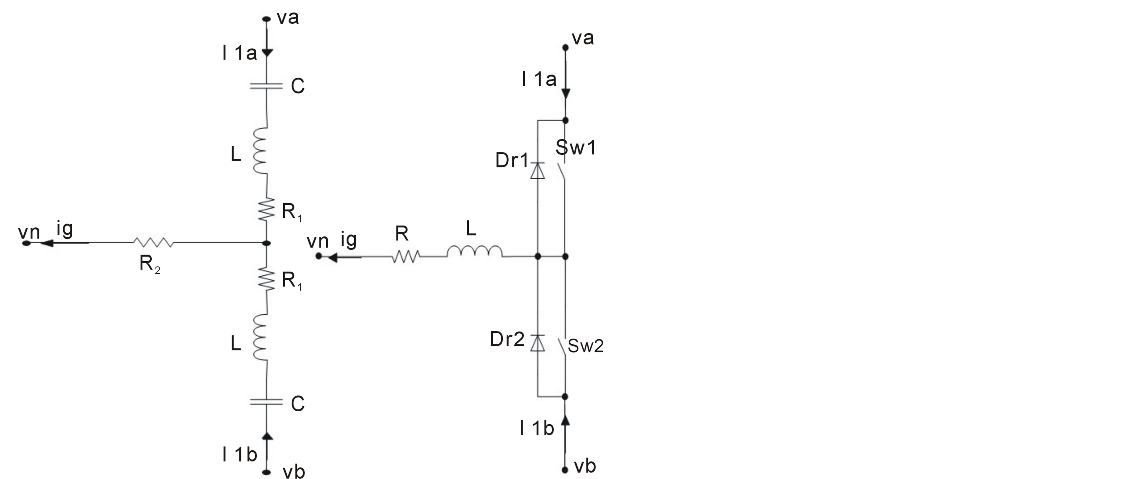
Various method of the current injection network was presented in bibliography [13-15]. Figure 6(a) shows the current injection network using a tuned LC circuit. It uses two inductances with two capacitors tuned to resonant frequency of 3 Fe (150 Hz), the resistance limits the injected current.
3.3. New Design Circuit Third Harmonic Current Injection
Figure 6(a) shows the standard current injection network which uses a tuned LC filter. That type of circuit can’t modify the frequency of the injected current, it uses two inductances with two capacitors tuned to resonant frequency of 3 Fe (150 Hz); the resistance limits the injected current. The formula of the resonant circuit is given by:
 (12)
(12)
where L = 60 mH and C = 18.75 µF.
The new design uses a switching device to modify the injected current as shown in figure 6(b).
The inductor L in figure 6(b) is used as a current generator source. The current waveform is generated by the activation of two switches; the first one creates the positive form of the injected current and the second one creates the negative form.
Both of the two switches are controlled using a simple logic control. Figure 7 illustrates the current injection network with the logic control used to create the third
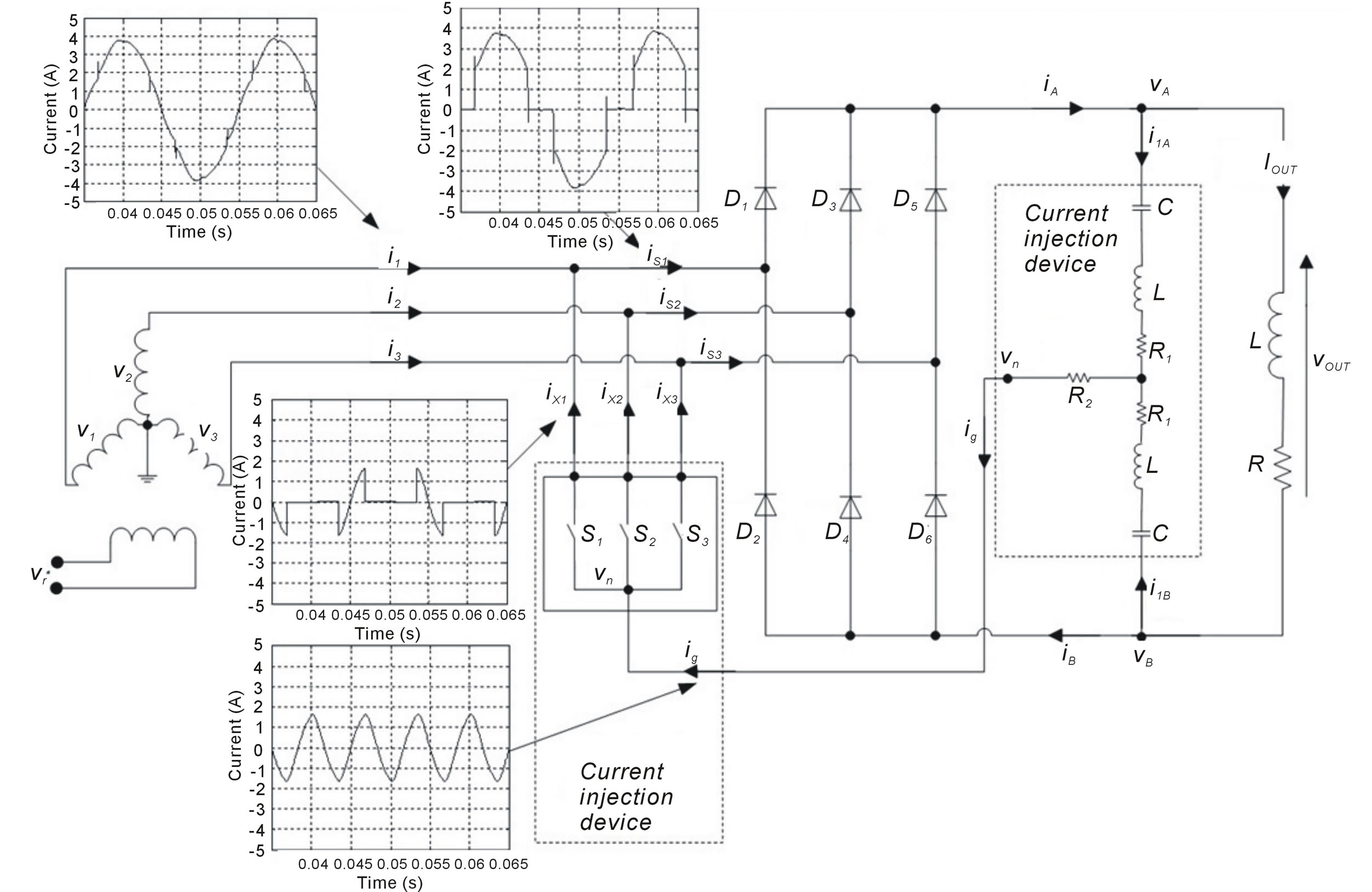
Figure 3. General scheme of harmonic injection method.

Figure 4. Switching current injection device.

Figure 5. Injection device circuit.
harmonic injected current.
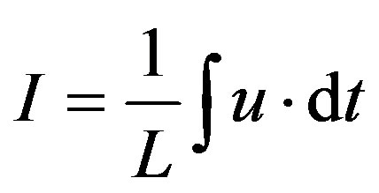
The current flowing through the inductance L can be written as follows:
 (a) (b)
Figure 6. Standard and new design current injection networks. (a) Usng tuned LC circuit. (b) Using a switching device.
 (13)
(13)
while the voltage across it is given by:
 (14)
(14)

Figure 7. Injection network with logic control.
The choice of L reflects the slope of the current desired reference; decreasing of this inductance is limited by the switching frequency of the injection circuit. The control logic of the injection system operates in a Schmitt trigger laws; it is described in figure 8.
4. Thermal Modeling of the Power Hybrid Module
Because most of the semiconductor device models are implemented in circuit simulators, thermal circuit networks are the practical models for electro-thermal simulations.
Literature proposes some approaches to construct thermal networks equivalent to a discretization of the heat equation. For example the finite difference method (FDM) and the finite element method (FEM) are proposed. In the case of vertical power devices, where the thickness LSI is small, compared to other dimensions, it is commonly considered that heat is generated at the top surface of silicon and flows uniformly along the x-axis (perpendicular to the silicon surface). So, the top surface is considered to be a geometrical boundary of the device at x = 0, where the input power P0(t) is assumed to be uniformly dissipated. In our case we have chosen the (FEM) technique to develop the thermal model of the Diode structure. Each material is represented by a simplified 1D thermal model. For the insulation and baseplate layer, a modification have been introduced on the 1D model to take into account the mutual thermal between the different components.
The thermal model of the silicon material can be represented by the equivalent electrical circuit [16-18] shown in figure 9 where:


Figure 8. Control logic of the injection system.
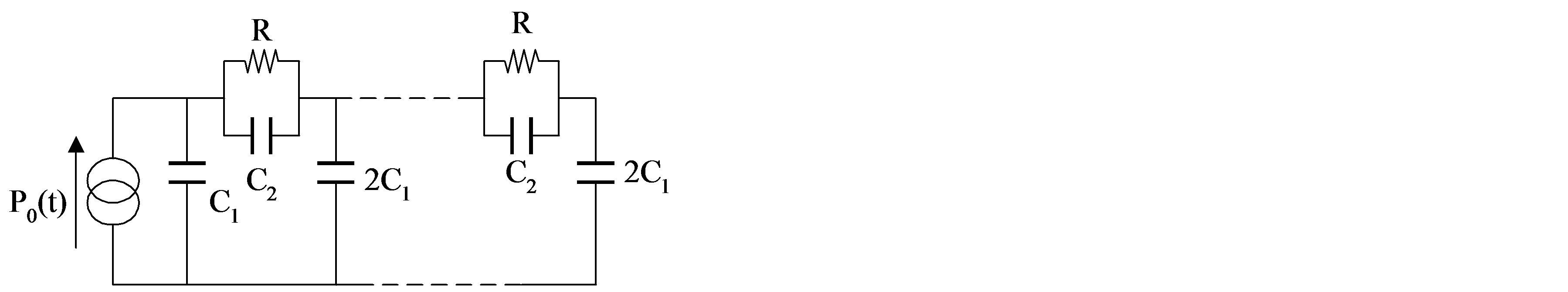
Figure 9. The 1D FEM thermal model of the silicon material.
while n is the number of nodes in the material model.
The thermal investigation was performed with the power diode BYT 12P-1000 (12 A/1000 V) (TO220 package) [19,20].
The superposition technique is used to develop the simplified thermal model of the Diode structure. The method simply requires that for each present independent heat source, one test must be performed. During each test, junction temperatures for all devices must be measured [21,22].
The thermal model of the components is implemented in the MATLAB simulator (MATLAB, 2010) in order to estimate the junction temperature of the DIODE. Figure 10 shows the evolution of the maximum junction temperature and the module base-plate temperature in the diode as a function of the dissipated power magnitude. These results are obtained by 1D thermal model, by experiments and by 3D numerical simulations in stationary conditions. A good agreement between the results of evolution is observed. From the results, it can be deduce that the proposed thermal model is valid.
Figure 11 shows a diagram of an electro-thermal simulation technique of power diode modules. An electrical model is coupled with a thermal one. The instantaneous value of the device power loss is injected into the thermal model in which the thermal characteristics of the module are defined. Then, the instantaneous device temperature is generated by the thermal model and the temperatures of the dependent device model parameters are determined via this instantaneous device temperature. These calculations are performed simultaneously using a circuit simulator. The device and the thermal models are

Figure 10. The DIODE maximal junction and base-plate temperature as a function dissipated power magnitude (ambient air 298 K).

Figure 11. Electro-thermal coupling diagram simulation.
essential components of the electro-thermal simulation. This diagram is used to estimate the losses in semiconductors switches; it is modeled in SIMULINK/MATLAB environment.
5. Simulation Results and Discussion
The standard circuit injection method works at a fixed speed. The simulation results are shown in figure 12. The source currents i1 and iS1 and the injected current iX1 are respectively shown in figures 12(a)-(c). The THD of the source current is shown in figure 12(d). We perceive a low harmonic distortion at a low speed.
The new design of circuit injection network, shown in figure 6(b) uses two switches to generate the injected current. At a variable speed, we change the current reference frequency; the Current injection network control tries to follow the current reference. Figure 13 shows the simulation results of the new Current injection network control circuit design; the injected current is very close to the reference current. We use a zoom to focus the form of the injected current and the commutation of the two switches. SW1 is used only at the positive form of the injected current, while SW2 is used at the negative wave form.
Figure 14 shows the harmonic spectrums of the classical PFC and the proposed PFCVF. We simulate both of the two circuits at different speeds from 1000 to 6000 rpm.
The variation of the harmonic currents according to
 (a)
(a)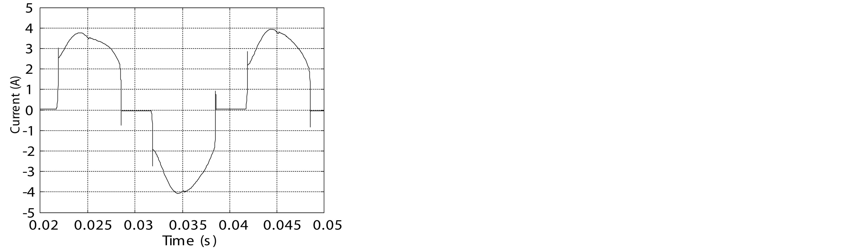 (b)
(b) (c)
(c) (d)
(d)
Figure 12. simulation results of standard circuit injection method. (a) Source current i1; (b) Source current iS1; (c) Injected current iX1; (d) THD of the source current.
the order of harmonic for the classical PFC and the proposed PFCVF is respectively shown in figures 14(a) and (b) for 1000 rpm respectively, figures 14(c) and (d) for 3000 rpm, and figures 14(e) and (f) for 6000 rpm.
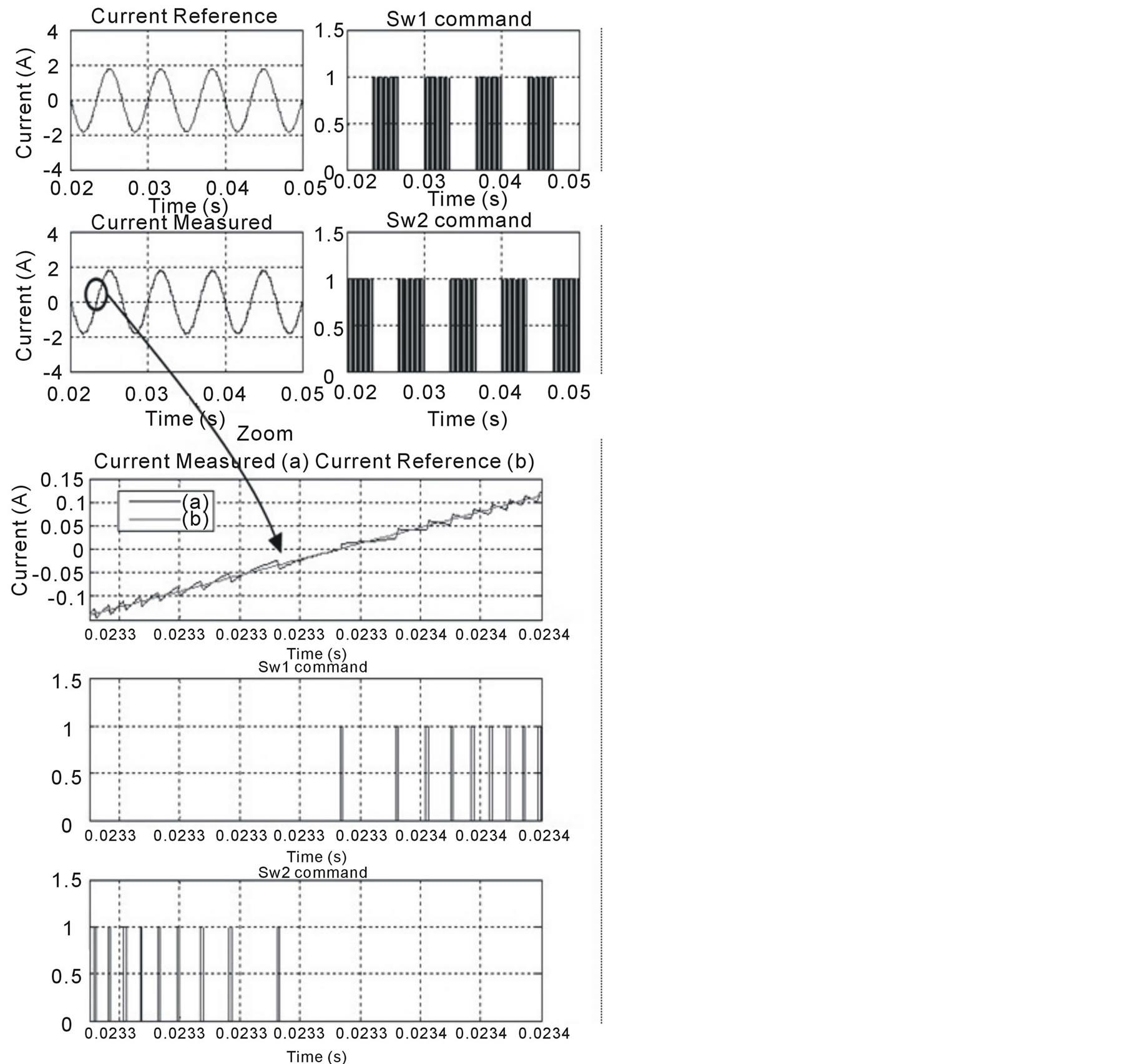
Figure 13. Simulation results of the new Current injection network control circuit design.
 (a)
(a)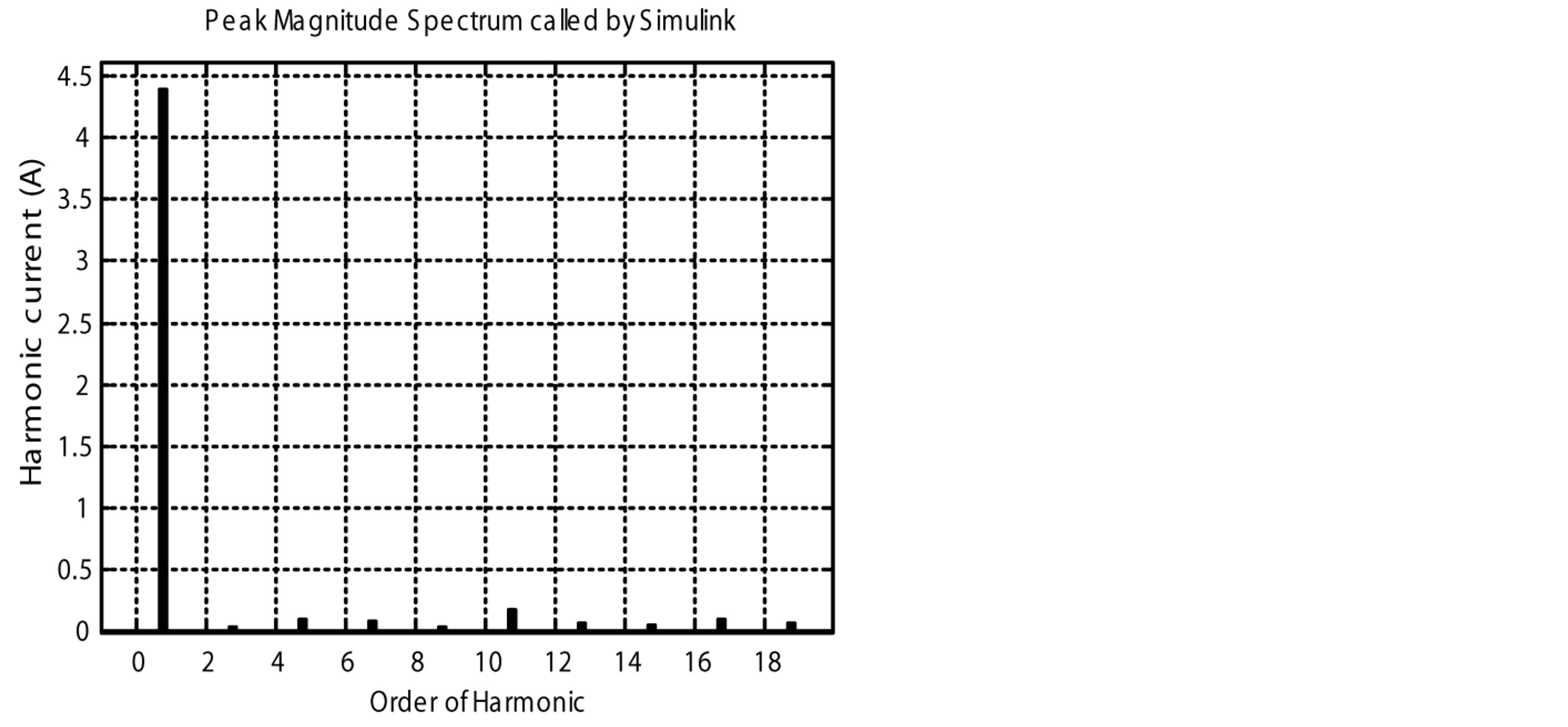 (b)
(b) (c)
(c)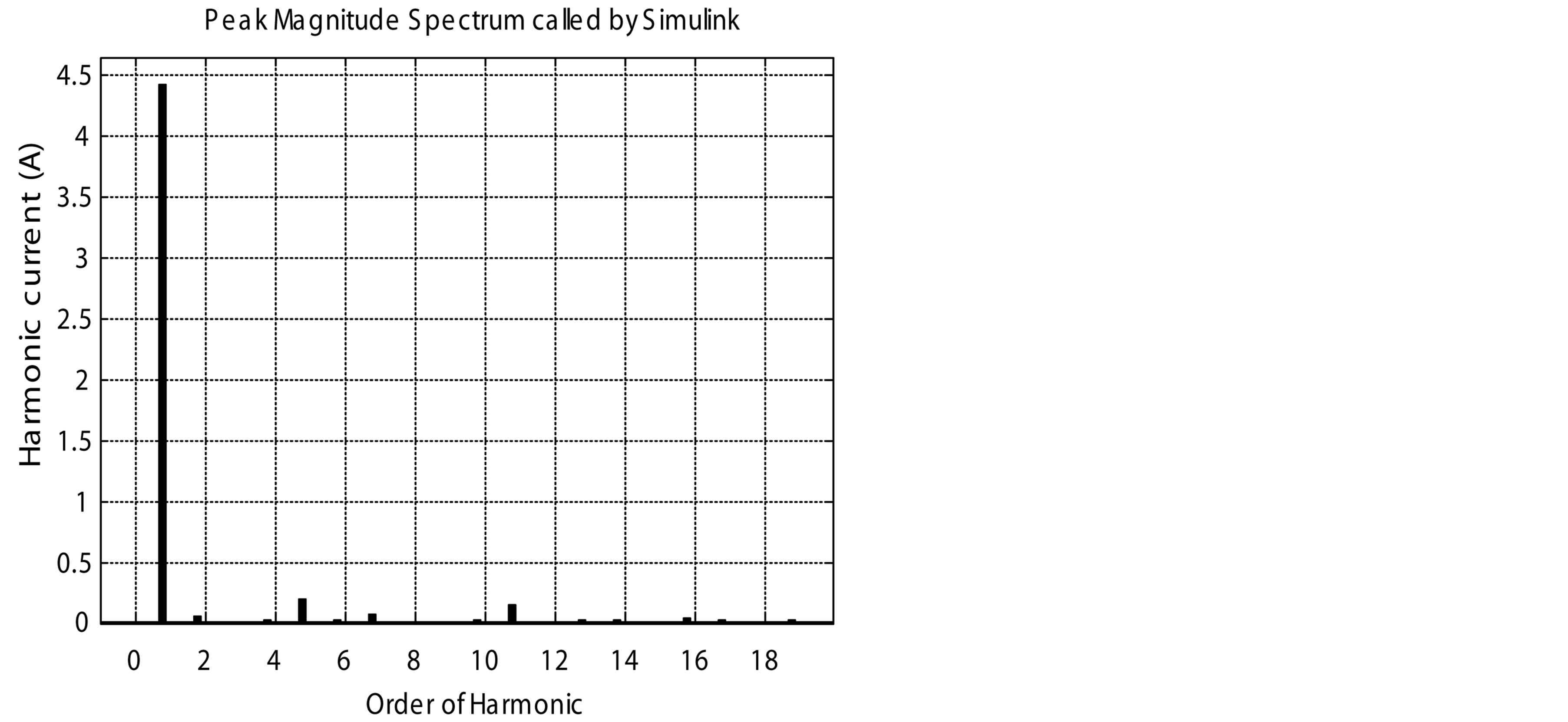 (d)
(d) (e)
(e) (f)
(f)
Figure 14. Harmonic spectrums of the classical PFC and the proposed PFCVF. (a) Harmonic spectrum of the classical PFC for 1000 rpm; (b) Harmonic spectrum of the proposed PFCVF for 1000 rpm; (c) Harmonic spectrum of the classical PFC for 3000 rpm; (d) Harmonic spectrum of the proposed PFCVF for 3000 rpm; (e) Harmonic spectrum of the classical PFC for 6000 rpm; (f) Harmonic spectrum of the proposed PFCVF for 6000 rpm.
As shown in Table 1 for 1000 rpm, the proposed PFCVF, presents a THD of 7.4% slightly higher than the classical PFC with a THD of 5.4%. For 2000 rpm; the proposed PFCVF, presents a THD of 5.89% better than the classical PFC with a THD of 11.29%. For 6000 rpm, the proposed PFCVF, presents a THD of 7.35% better than the classical PFC with a THD of 18.21%.
At low speed, the THD is slightly lower in the standard injection circuit; in fact the new current injection network generates a high frequency noise due to the commutation of SW1 and SW2; but at a high speed this commutation noise is insignificant compared to the

Table 1. THD of the classical PFC and the proposed PFCVF.
disharmony caused by the standard current injection network. The proposed PFCVF strategy reduces the THD in the machine phase current. Indeed, it improves output voltage, and reduces output total harmonic distortion and voltage stress on semiconductors switches. By adopting PFCVF strategy the THDI value is reduced to 7.35% all over the machine speed.
Figure 15 shows the motor electromagnetic torque evolution as a function of time, obtained by the classical PFC and the proposed PFCVF corresponding to 3000 rpm.
These results show that the machine torque, in the case of classical PFC, presents a ripple over 60% against 10% in the case of the proposed PFCVF. The proposed PFCVF strategy decreases the machine torque ripple.
Figure 16 shows the temperature variation of the case and the diode junction. Figure 16(a) shows the evolution of the maximal junction temperature in the diode. In the thermal simulation two different rectifiers are used: classical rectifier and PFCVF one. It is clear that the diode junction temperature obtained by PFCVF is lower than that obtained by the classical rectifier. For example, at a time equal to 0.15 s, the diode junction temperature obtained by PFCVF rectifier is equal to 327 K whereas the diode junction temperature obtained by classical PFC is equal to 330 K.
Figure 16(b) shows the evolution of the case temperature. We clearly see that the diode case temperature obtained by PFCVF rectifier is lower than that obtained by the classical PFC. It proves that the use of the PFCVF rectifier reduces the losses in the semiconductors switches. The PFCVF rectifier can be used for a very high power application which needs low stress on power devices as diodes.
6. Experimental Evaluation
To verify the analytically obtained results, a 1kW rectifier is built; a synchronous machine is used as an alternator to create the three phase voltage system. Figure 17 shows the experimental devices; the alternator is coupled with a controlled DC motor to allow controlling the speed and thus the output signal frequency as shown in figure 17(a).
The output voltage can be adjusted using a rheostat cabled in a serial way with an excitation source. The current injection network is shown in figure 17(b).

Figure 15. Torque ripple of the alternator.
 (a)
(a)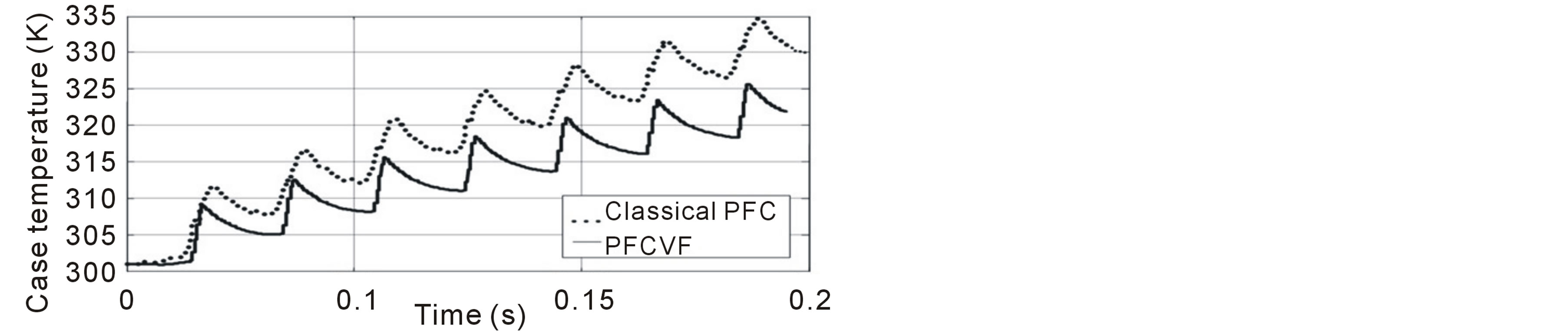 (b)
(b)
Figure 16. Variation of the temperature of the case and the diode junction. (a) Junction temperature (K); (b) Case temperature (K).
The current injection network uses two 20 mH inductors and two 100 µF capacitors; the frequency of the resonant circuit is 112 Hz, we had to use a frequency of 37 Hz as a voltage source. The output voltage is fixed to 100 V; a 42 Ω power resistor is used as a charging system and consumes about 4A as an output current.
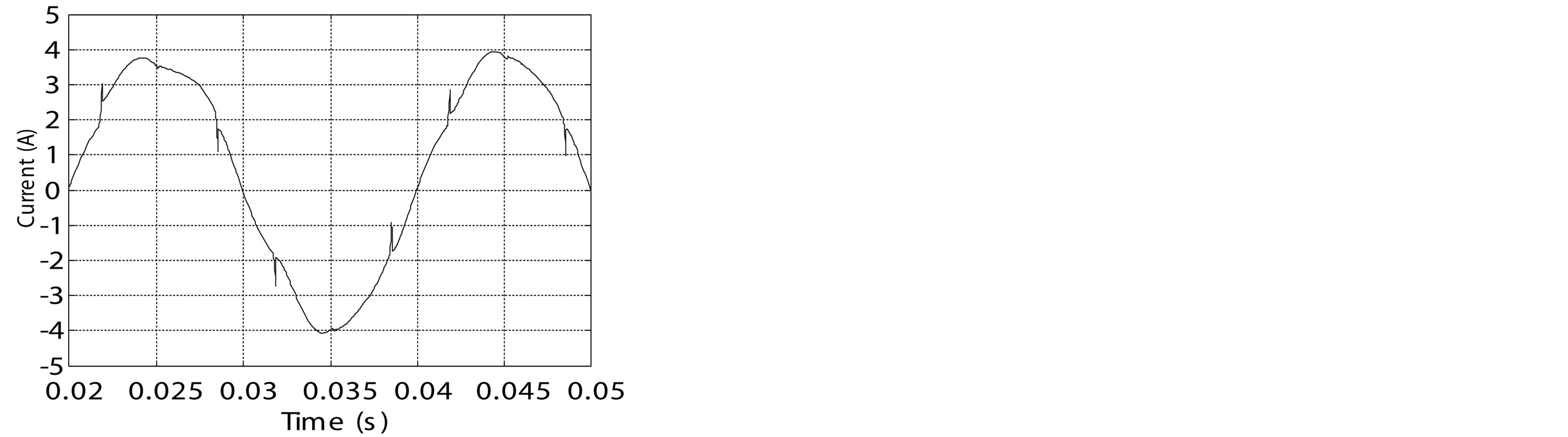
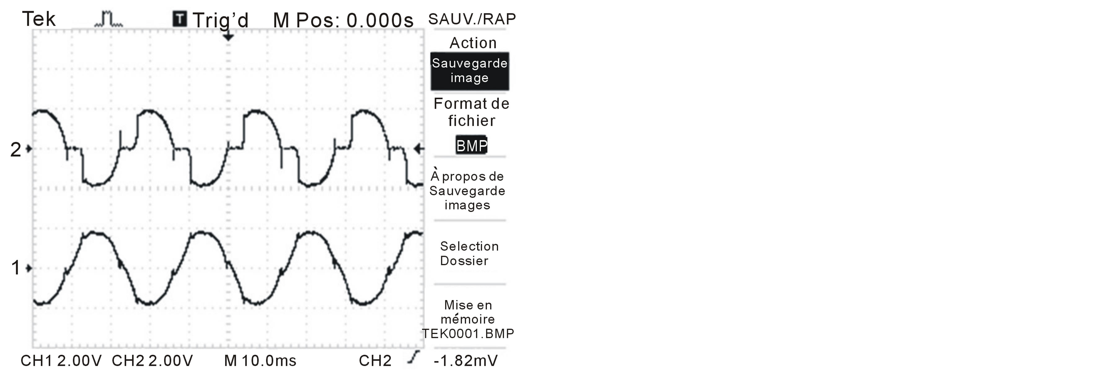
The current results are shown in figure 18. The waveforms of i1 and iS1 are respectively represented in figures 18(a) and (b). The waveform of i1 corresponds to the current which is with injection; we see that it is less polluted by harmonics than the iS1 waveform which is without injection.
The voltage results are shown in figure 19. V1 and VS1 waveforms are respectively represented in figures 19(a) and (b). The waveform V1 corresponds to the current with injection, and we see clearly that it is less polluted
 (a)
(a) (b)
(b)
Figure 17. Experimental devices. (a) Synchronous alternator coupled with a DC motor; (b) Switching Current Injection device.
 (a)
(a) (b)
(b)
Figure 18. Current results. (a) Source current iS1 and i1 using injection circuit; (b) Source current iS1 and i1 without injection circuit.
 (a)
(a)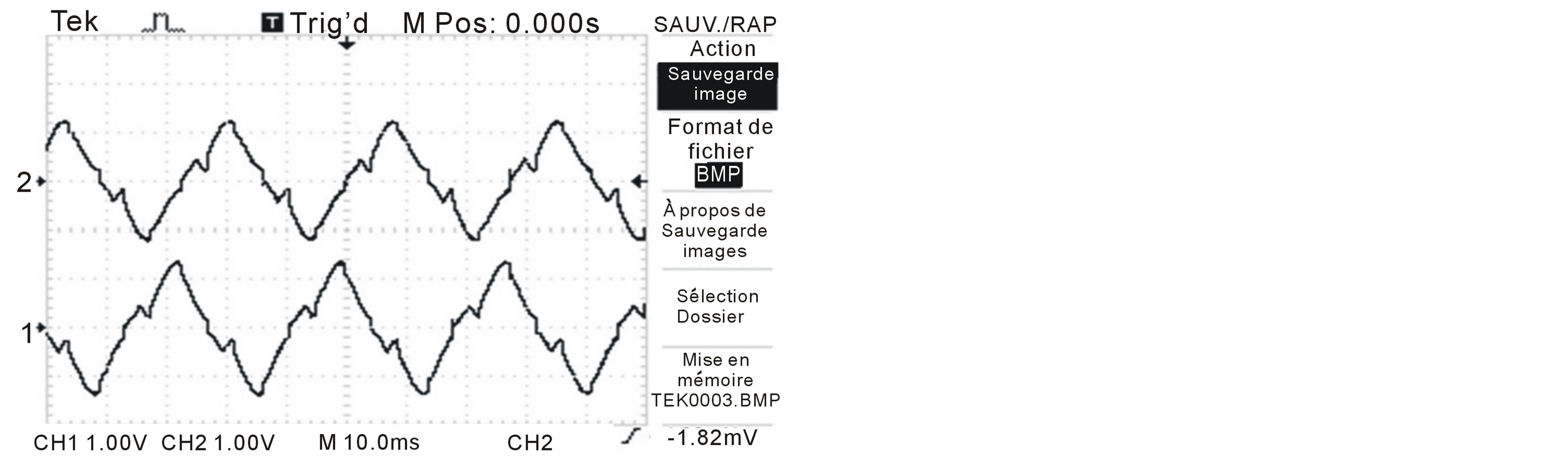 (b)
(b)
Figure 19. Voltage results. (a) Source voltage V1 and V2 using injection circuit; (b) Source voltage V1 and V2 without injection circuit.
by harmonics than the VS1 waveform which is without injection.
7. Conclusion
In this paper, we presented a PFC rectifier that uses a variable frequency source for electric vehicle application. Comparisons between fixed frequency circuit and variable frequency voltage source are presented. Results prove that the PFCVF strategy reduces the THD. It improves output voltage, and reduces the output total harmonic distortion and voltage stress on semiconductors switches. By adopting the PFCVF strategy, the THD value is reduced by more than 50%, the Diode junction temperature value is decreased to 335 K. The experimental results highlight the effectiveness of the proposed design.
REFERENCES
- M. Malinowski, M. Jasinski and M. P. Kazmierkowski, “Simple Direct Power Control of Three-Phase PWM Rectifier Using Space-Vector Modulation (DPC-SVM),” IEEE Transactions on Industrial Electronics, Vol. 51, No. 2, 2004, pp. 447-454. http://dx.doi.org/10.1109/TIE.2004.825278
- S. Choi, A. R. von Jouanne, P. N. Enjeti and I. J. Pitel, “Poliphase Transformer Arrangements with Reduced kVA Capacities for Harmonic Current Reduction in Rectifier Type Utility Interface,” Proceedings of 26th Annual IEEE of Power Electronics Specialists Conference, Vol. 1, Atlanta, 18-22 June 1995, pp. 353-359.
- A. Z. Javad and S. Moghani, “Design and Implementation of a novel Vector-Controlled Drive by Direct Injection of Random Signal,” International Review of Electrical Engineering (IREE), Vol. 4, No. 6, 2009, pp. 1198-1203.
- A. Toumi, M. Ghariani, I. Ben Salah and R. Neji “ThreePhase PFC Rectifier Using a Switching Current Injection Device for Vehicle Power Train Applications,” International Journal of Electrical Engineering and Transportation, Vol. 6, No. 2, 2010, pp. 15-18.
- M. Malinowski, M. Jasinski and M. P. Kazmierkowski, “Simple Direct Power Control of Three-Phase PWM Rectifier Using Space-Vector Modulation (DPC-SVM),” IEEE Transactions on Industrial Electronics, Vol. 51, No. 2, 2004, pp. 447-454. http://dx.doi.org/10.1109/TIE.2004.825278
- P. Rioual, H. Pouliquen and J. P. Louis, “Regulation of a PWM Rectifier in the Unbalanced Network State Using a Generalized Model,” IEEE Transactions on Power Electronics, Vol. 11, No. 3, 1996, pp. 495-502. http://dx.doi.org/10.1109/63.491644
- H. Song and K. Nam, “Dual Current Control Scheme for PWM Converter under Unbalanced Input Voltage Conditions,” IEEE Transactions on Industrial Electronics, Vol. 46, No. 5, 1999, pp. 953-959. http://dx.doi.org/10.1109/41.793344
- P. Xiao, K. A. Corzine and G. K. Venayagamoorthy, “Multiple Reference Frame-Based Control of ThreePhase PWM Boost Rectifiers under Unbalanced and Distorted Input Conditions,” IEEE Transactions on Power Electronics, Vol. 23, No. 4, 2008, pp. 2006-2017. http://dx.doi.org/10.1109/TPEL.2008.925205
- M. Ayadi, El M’Barki, M. Ghariani and R. Neji “A Comparison of PWM Strategies for Multilevel Cascaded and Classical Inverters Applied to the Vectorial Control of Asynchronous Machine,” International Review of Electrical Engineering, Vol. 5, No. 5, 2010, pp. 2106-2114.
- J. I. Itoh and I. Ashida, “A Novel Three-Phase PFC Rectifier Using a Harmonic Current Injection Method,” IEEE Transactions On Power Electronics, Vol. 23, No. 2, 2008. http://dx.doi.org/10.1109/TPEL.2007.915774
- W. L. Soong and N. Ertugrul, “Inverterless High-Power Interior Permanent-Magnet Automotive Alternator,” IEEE Transactions on Industry Applications, Vol. 40, No. 4, 2004, pp. 1083-1091. http://dx.doi.org/10.1109/TIA.2004.830773
- M. Ghariani, A. Ltifi, I. Ben Salah, M. Ayadi and R. Neji “New Sliding-Mode Observer for Induction Machine in Electric Propulsion Applications,” International Review on Modelling and Simulations, Vol. 3, No. 4, 2010, pp 493-501.
- Y. Li, F. C. Lee, J. Lai and D. Boroyevich, “A Novel Three-Phase Zero-Current-Transition and Quasi-ZeroVoltage-Transition (ZCT-QZVT) Inverter/Rectifier with Reduced Stresses on Devices and Components,” IEEE 2000, pp. 1030-1036.
- P. Pejovic, J. W. Kolar and Y. Nishida “Bidirectional Ac-Dc Converter for Regenerative Braking,” 16th International Symposium on Power Electronics, Vol. 6, No. 1, 2012, 8 Pages.
- B. Singh, B. N. Singh, A. Chandra, K. Al-Haddad, A. Pandey and D. P. Kothari, “A Review of Three-Phase Improved Power Quality AC-DC Converters,” IEEE Transactions on Industrial Electronics, Vol. 51, No. 3, 2004, pp. 641-660. http://dx.doi.org/10.1109/TIE.2004.825341
- A. Rufer, M. Veenstra and K. Gopakumar, “Asymmetric Multilevel Converter for High Resolution Voltage Phasor Generation,” Proceedings of the 1999 EPE Conference, Lausanne, 7-9 September 1999, pp. 1-10.
- K. A. Corzine, “A Hysteresis Current-Regulated Control for Multi-Level Drives,” IEEE Transactions on Energy Conversion, Vol. 15, No. 2, 2000, pp. 169-175. http://dx.doi.org/10.1109/60.866995
- A. Ammous, B. Allard and H. Morel, “Transient Temperature Measurements and Modeling of IGBT’s under Short Circuit,” IEEE Transaction Electronic Devices, Vol. 13, No. 1, 1998, pp. 12-25.
- E. Farjah, Ch. Scheffer and R. Perret, “Experimental Thermal Parameter Extraction Using Non-Destructive Tests,” EPE, Sevilla, 1995, pp. 1245-1248.
- M. Ludwig, A. Gaedke, O. Slattery, J. Flannery and S. C. Mathuna, “Characterisation of Cooling Curve for Power Device Die Attach Using a Transient Cooling Curve Measurement,” 0-7803-5692-6/00/$10.00 (c) 2000 IEEE, pp. 1612-1617.
- M. Ayadi, M. A. Fakhfakh, M. Ghariani and R. Neji, “Electrothermal Modeling of Hybrid Power,” Microelectronics International, Vol. 27, No. 3, 2010, pp. 170-177. http://dx.doi.org/10.1108/13565361011061993
- M. Ayadi, M. A. Fakhfakh, M. Ghariani and R. Nej, “Electro-Thermal Simulation of a Three Phase Inverter with Cooling,” Journal of Modelling and Simulation of Systems, Vol. 1, No. 3, 2010, pp. 163-170.
Nomenclature
Rs: Stator resistance per phase (=1.4535 Ω)
Vds, Vqs: d-axis and q-axis stator voltage Ids, Iqs: d-axis and q-axis stator current Lr: Rotor inductance per phase (=0.0144 H)
Ls: Stator inductance (=0.0145 H)
M: Mutual inductance of stator and rotor (=0.0130 H)
 : Total leakage factor
 : Stator time constant
Φr: Rotor Flux
ωs: Synchronisation speed Rr: Rotor resistance per phase referred to stator (=1.4161 Ω).
ωm: Electromechanical angular velocity of the motor
ωg: Electric slip speed
Φs: Stator flux A: Surface of the silicon material K: Thermal capacity of the silicon material LSI : Thickness of the silicon material
Ρc: Thermal conductivity of the silicon material