Materials Sciences and Applications
Vol.4 No.8A(2013), Article ID:35814,11 pages DOI:10.4236/msa.2013.48A001
Self-Organizing Processes in Semiconductor Materials Science on the Example of Nanostructuring of por-Si*
![]()
Institute of Physics and Technology, Almaty, Kazakhstan.
Email: #kt011@sci.kz
Copyright © 2013 Kurbangali B. Tynyshtykbaev et al. This is an open access article distributed under the Creative Commons Attribution License, which permits unrestricted use, distribution, and reproduction in any medium, provided the original work is properly cited.
Received June 13th, 2013; revised July 12th, 2013; accepted July 23rd, 2013
Keywords: porous silicon; point defects; self-organization; nanostructuring
ABSTRACT
Self-organization processes in semiconductor materials on the example of nanostructuring of por-Si at long anodic etching of p-type Si in the electrolyte with internal source of the current are shown. In conditions of a “soft” etching of the Si point defects are formed and in the subsequently occurs their spatial-temporal ordering. This leads to the ordering pores and the nanostructuring of por-Si. Self-organization mechanism of Si nanocrystallites islets is described by the effects of the elastically-deformative, defectively-deformative and capillary-fluctuation forces.
1. Introduction
The progress of materials science associates with the nanostructures (NS) and requires completely new approaches for their creation. The NS are formed by using the self-organization processes and must be highly homogeneous on form, sizes and relative position. And most importantly, they must be paired with traditional technology of microand nanoelectronics.
All these lead to the development of various methods of the initial surface modification for intensification of the growth and self-organization of the NS and receiving compatible nanostructuring layers.
Earlier [1], we received the highly ordered mosaic structure (MS) of por-Si, consisting of 3D islets ensemble of Si nanocrystallites (Si-NCs), using the self-organizing processes at long anodic etching of p-Si (100) in the HF-electrolyte with addition of the hydrogen peroxide.
Significant role in all self-organization processes of nanostructuring on the real solid surface is given to longrange elastically-deformative forces [2,3].
As will be shown on the example of self-organization of the MS por-Si, consisting of 3D islets ensemble of Si-NCs por-Si [1,4,5], in addition to commonly accepted elastically-deformation forces [2,3], the additional action of defectively-deformative [6] and capillary-fluctuation [7,8] forces must be considered.
Besides, self-organizing processes of the nanostructuring occur spontaneously on real defective surface of the crystal at the certain macroscopic conditions. Therefore, consideration of influence of macroscopic experimental conditions on the self-organizing processes of the nanostructuring and of the NS growth is interesting for study.
Such consideration submitted on the example of selforganization of highly ordered MS of por-Si, which occurs in conditions of “soft” electrochemical etching of pSi (100) in the electrolyte with internal source of the current (EISC).
2. Experimental Technique
Soft Etching Conditions in the Electrolyte with Internal Source of the Current
In experiments p-Si (B) samples with the orientation (100), resistivity of 0.01 Ω∙cm and thickness of 350 μm were used. Indium ohmic contacts were made on the backside of p-Si wafer by thermal annealing at 300˚C for 30 min. The anode was the p-Si, the counter electrodeNi, with thickness of 500 μm. Electrochemical etching conducted in the electrolyte containing HF (49%): H2O2
(40%) = 1:1 with a strong oxidizer. Etching time varied from 1 min to 240 min. Density of anode current was about ja = 1.7 mA/cm2 [4].
In such of the electrochemical system, Ni/HF-H2O2/pSi, take place the internal difference of electric potential in the process etching and arises electromotive force (emf), the internal current source [9]. Etching of silicon occurs in the conditions of “soft” influence, when takes place the equilibrium formation of pores in contrast from the etching with an external current source, when this condition does not be carried out.
Samples after etching and washing in distilled water were dried and stored in a desiccator with silica gel and pre-heated at 200˚C.
Atomic force (JSPM-5200) and scanning electron (JSM-6490LA) microscopes were used for the electron microscopy studies of por-Si surface morphology. Measurements on the atomic force microscope were conducted by semi-contact mode of AFM-AC, using cantilevers of MicroMasch NSC35AlBS Company.
3. Experimental Results
Self-Formation of MS por-Si
The self-organization of highly ordered MS por-Si of 3D-islets Si-NCs is observed at the long-term (tetch. = 240 min) etching of p-Si(100) (figure 1).
MS por-Si consists of the ensemble of 3D islets of threadlike Si-NCs. Islets represent ensembles of the oxidized NCs por-Si and are separated by silicon ledges [4]. The distances between the islets of oxidized Si-NCs por-Si are 1 - 2 μm, and the period of the islets locations is about 20 μm.
The nucleation of such MS por-Si is preceded by the formation of homogeneous nanoporous layers with thicknesses dpory = 1, 2, 4, 7, 18, 20 μm at the etching times tetch. = 1, 2, 5, 15, 30, 45 min, respectively. However, when etching time 45 min or more thickness of nanoporous layers remains 20 μm.
Figure 2 shows the electron microscopic image of por-Si surface after с-Si etching for 30 min, on which can be seen uniformly distributed nanopores (diameter is about 10 nm).
The formation of the secondary porous layer is observed with increasing etching time up to tetch = 60 min (figure 3).
On figure 3 are seen the plots of porous silicon in the form of separate islets of Si-NC por-Si and continuous layer.
At the further etching (tetch = 60 min) the formation of cracks in the form of a netted texture (NT) of a surface with a specific crystallographic orientations occurs (figure 4).
NT of por-Si surface with further etching (tetch. = 120
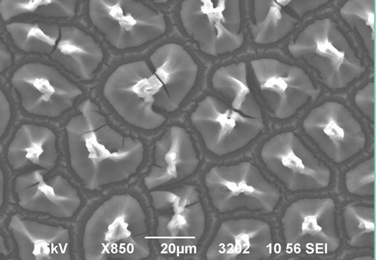
Figure 1. Electron microscope image (JSM6490LA) of MS por-Si [1]. Sample p-Si (100) with resistivity of 0.01 Om·sm. Electrolyte—HF(49%):H2O2(40%):H2C5OH = 1:1:1, etching time tetch = 240 min.
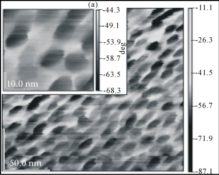
Figure 2. Atomic Force Microscope Image (JSPM5200) of por-Si (100) surface after etching p-Si (100) in HF (49 wt%): H2O2 (40 wt%), tetch = 30 min [5].
min or more) is transformed into the MS (figure 1).
Figure 5 shows the electron microscopic image of por-Si surface after tetch. =120 min, on which presents the different plots of etching due to the no uniformity of Si sample etching.
Etching rate is more in the central part of the sample, than at the periphery. Nonuniform etching of the porous surface sample lets to track on this figure practically is observed all main stages of MS por-Si origin. On the figure, on the periphery of the sample, due to the lower etching rate, can see initial stage of formation of the quasiparallel cracks, located at distance of about 20 μm from each other, along the crystallographic direction [010] can be seen. Closer to the sample center, where efficiency of etching grows, these cracks [010] are crossed with arising transverse cracks along [001]. Further development of these cracks along axes <010> and
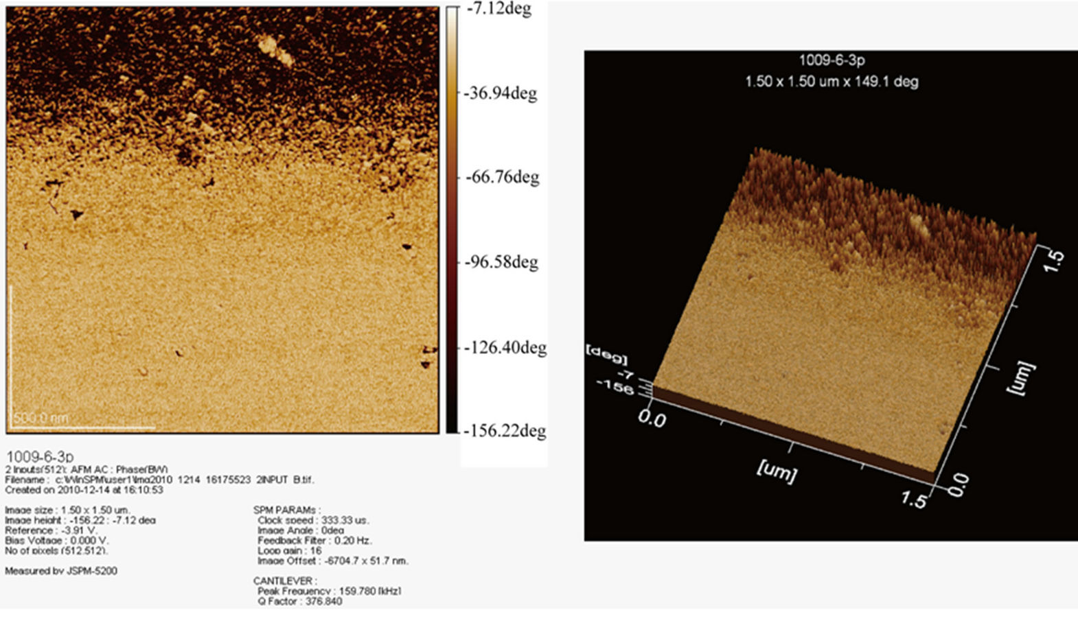
Figure 3. Atomic-force image of the secondary porous layer formation on surface p-Si (100), tetch = 60 min.

Figure 4. Electron microscope image of netted texture cracks on por-Si surface etched in p-Si (100), HF (49 wt%): H2O2 (40 wt%), during tetch = 60 min.
<001> leads to the formation of NT (figure 3). In the central part of the sample MS por-Si in the form of planar shape irregular, separated by ledges is partially observed. Cell bottom, which free from the remote SiNCs islets por-Si, visible in some places, allows observing quite well formed ledges. On silicon ledges of MS por-Si, the cracks with characteristic orientation have also been observed (figure 6).
Electron-microscope image of surface topography of por-Si at different magnifications is shown in figure 7. This allows us to see hillocks and hollows, which repeat in the form of dendrite-like structures.
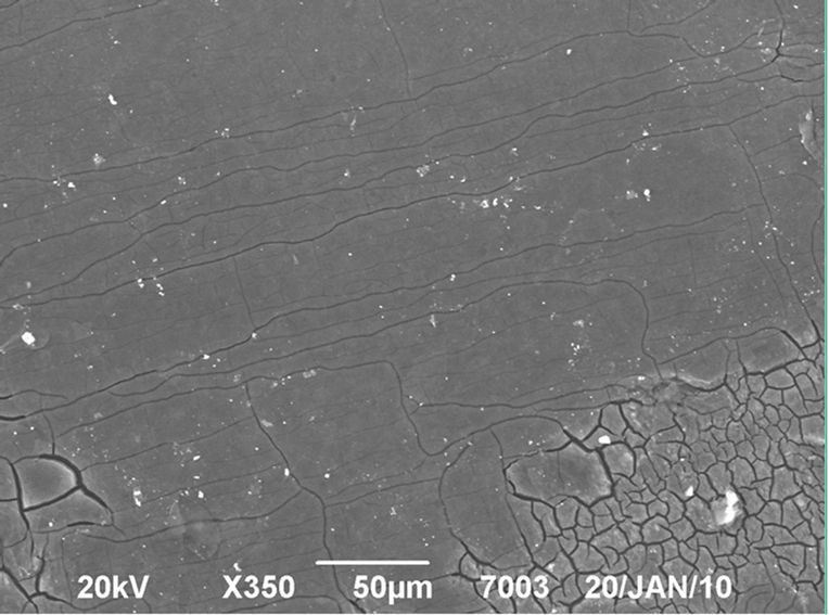
Figure 5. Electron microscope image of quasiparallel cracks on porous surface of the p-Si (100) along the <010> and <001> crystallographic axes. Samples of p-Si (100) etching in HF (49 wt%): H2O2 (40 wt%), tetch = 120 min.
MS por-Si is not observed in similar experiments at the long-term etching (up to tetch.= 240 min or more) of p-Si wafers with the plane (111).
Further etching leads to the formation of highlyordered MS por-Si in the form of islets from the oxidized Si-NCs separated by silicon ledges (figure 8).
The conducted element analysis of islets, cells and separation of their ledges showed that islets represent clusters of the oxidized Si-NCs, but the cells, bottom and ledges consist of c-Si [4].
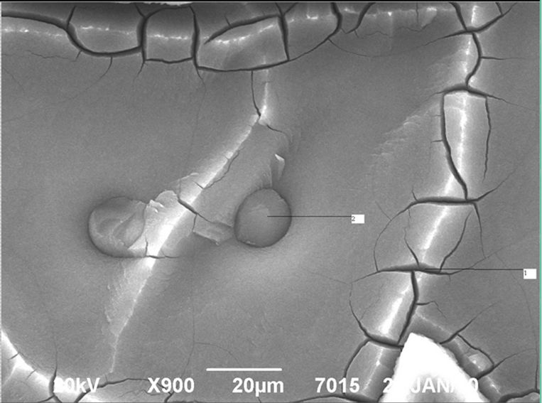
Figure 6. Electron microscope image of cracks on silicon ledges of p-Si (100) porous surface <010> and <001> along the crystallographic axes. Samples of p-Si (100), HF (49 wt%): H2O2 (40 wt%), tetch = 120 min [5].
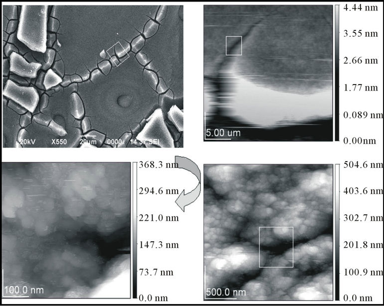
Figure 7. Electron microscope image of the fractal surface of cluster NCs por-Si islets at the different scales of magnification. p-Si (100), HF (49 wt%): H2O2 (40 wt%), tetch = 240 min.
Electron microscope image of the cross-section por-Si samples shows, that formation of 3D islets NCs MS porSi occurs in the form of the truncated tetrahedral pyramids (figure 9).
4. Discussion
4.1. Dynamics of the Nucleation and Formation of Silicon Ledges
Dynamics analysis of the nucleation and formation of MS from ensemble of 3D islets NCs por-Si in the form of the truncated tetrahedral pyramids shows, that on the basis of their appearance lies processes of the nucleation and formation of cracks on por-Si surface. For refinement of the formation mechanism of MS por-Si it is ne-
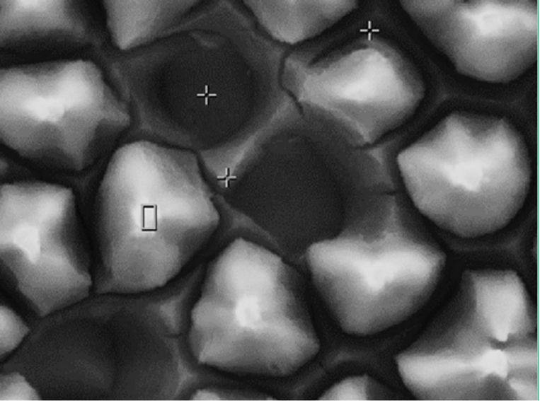
Figure 8. SEM image of the surface por-Si and elemental composition of different morphological parts after annealing at 300˚C [4]: islets with elemental composition—30.54% (Si), 51.81% (O), 17.65% (C); a residual trace of an island - 50.17% (Si), 35.09% (O), 14.75% (C); bottom of the cell - 66.64% (Si), 33.36% (O), C is not present; a ledge deepening- 88.45% (Si), 11.55% (O), C is absent. The electrolyte composition—H (49%):H2O2(40%):H2C5OH = 1:1:1.
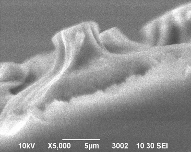
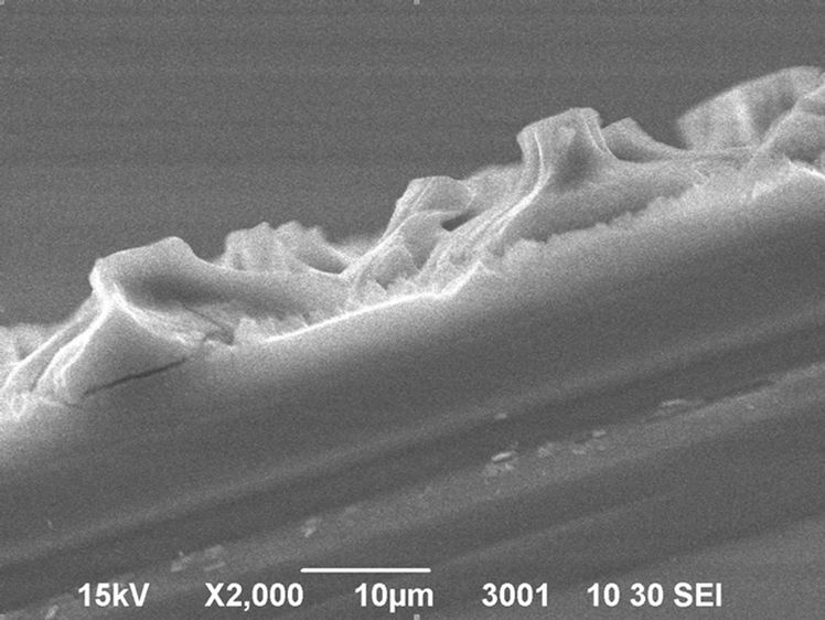
Figure 9. Cross-section electron-microscope image of por-Si samples (figure 1) with 3D islets NCs MS por-Si.
cessary to establish the nature of the crack appearance on the surface of porous p-Si (100) during its long-term etching.
Dynamics analysis of the nucleation and formation of cracks will begin with consideration of formation process of pores at long-term etching in EISC, in conditions of “soft” impact.
Electrolytic etching of Si in the solution of hydrofluoric (HF) acid, where oxidation and reduction reactions proceed with the formation of different products, consists of the large number of a multi-stage process of sequential and parallel reactions.
The main reactions are the following two consecutive flowing reactions [10]. First reaction is related with the consumption of holes h+, which leads to the formation of divalent ions Si+2
 .
.
Second reaction related either with the oxidation of Si+2. Formed ions Si+2 are unstable, further they are oxidized
 where X - H, O, F, ..., on example, with ions of hydrogen, oxygen, fluorine, and others, with the formation Si+4 and gaseous product X2.
Either participates in the disproportionation reaction, when in the result of charge exchange formed secondary neutral atoms Si0
 which are the structural defects of crystal lattice.
Thus, Si+4 and its steady connections with F, O and H in the form of various fluorides, oxides, and hydrides are formed.
These two reactions lead to the formation of pores on the crystal surface.
The formation process of pores at long anodic etching of monocrystals p-Si (100) in EISC proceeds on the initial stages of etching, after formation of structural defects of crystal lattice in form of Si0 and, respectively, vacancies, V.
Variety of pores depends on the crystallographic orientation of silicon. This is due to the difference in the packing density of atoms in the crystal along the crystallographic axes.
The density of Si atoms in the crystallographic direction [111] is much higher, than in the direction [100].
It defines a high speed of Si atoms removal in the process of etching of pores on the Si surface with the plane (100) [11].
At the same conditions of etching, electrochemical etching rate in the direction [111] is minimum because of the maximum packing density of atoms in the crystal lattice Si.
Secondary atoms Si0, formed at disproportionation reactions, transfer into the electrolyte solution, saturating it at long etching. At this occurs reverse deposition of neutral atoms Si0 on interporous space, forming the secondary porous layer.
A part of Si adatoms is recrystallized in Si-NCs por-Si, the other part remains in the form of an amorphous phase [11]. As a rule, their surface is covered by complex compounds of products of the anodizing and absorption reactions, including hydrides and oxides of silicon [12].
Thus, the secondary porous layer is formed from the precipitated aggregates adsorbed atoms (adatoms) Si0 and present of complex structures, consisting of an amorphous and recrystallized phases, covered by layers of hydrides and oxides silicon. And it represents the elastically-strained system due to the mismatch of the lattice parameters NCs of por-Si and the matrix с-Si with the secondary porous layer, in common .
This process of self-organizing ordered MS from ensemble of NCs-Si islets on the surface of por-Si (figure 1) in many aspects is similar to processes of epitaxial growth of thin films.
The interface (IF) electrolyte/por-Si/c-Si, containing nanopores (respectively Si-NCs), is a complex heterophase system. The IF between the individual Si-NCs/c-Si and the IF por-Si/c-Si is elastically strained and determines the appearance of long-range surface forces.
In the process of electrochemical etching Si is formed pointing defects (PDs) the interstitial silicon atoms (ISi), vacancies (VSi), accordingly. At long etching proceeds their spatial-temporal ordering, which affects the self-organization processes of por-Si nanostructuring.
Also, on the IF electrolyte/por-Si takes place fluctuation of the electric field of the local microscopic plots on the semiconductor surface, which also affects the selforganizing processes on it.
At long etching of p-Si (100), part Si0 can remain in a crystal, in the view of ISi and, accordingly, VSi, which are both by structural PDs of c-Si.
ISi diffuses faster, than VSi to different sinks and on large distances because of their high mobility [13]. VSi, as a rule, concentrates in the places of their formation on the surface c-Si, forming of pores nucleation centers [14,15].
In the case por-Si, sinks (runoff) for ISi are the IF Si-NCs por-Si/c-Si. In this case, the predominant direction of ISi displacement is the crystallographic directions with the lowest density of atoms packing of the crystal lattice [2]. For a cubic c-Si on the surface plane (100) is a typical direction [010] and [001].
VSi also moves to different sinks by replacing silicon atoms, but their diffusion rate is small, than the rate diffusion of ISi.
Therefore occurs a spatial-temporal separation ISi и VSi [6,13-15]. And as the result, there are elastic defectivelydeformative forces, directed from congestions concentrations of interstitial clusters to vacation complex. This leads to the additional deformation of the crystal surface and to formation of the wave relief surface in the form of ridges in places of ISi congestions, and hollows in places of VSi congestions [6,13-15].
At the achievement of critical thickness of a secondary porous layer [16-19] (a secondary porous layer por-Si) under influence of the elastic deformation forces occurs a relaxation of an elasticallystrained of secondary layer and formation of cracks in the form of the NT (figure 3).
Mechanism of the formation of cracks NT on por-Si p-Si(100) surface during long-term etching was researched by electron-microscopic study. The por-Si surface researched on the etching samples during 60 - 240 min. The etching time has been caused from the fact that in this interval occurs transformation of por-Si surface from cracking NT to MS.
In figure 5 it has been shown electron-microscope image of the por-Si sample surface after etching tetch. = 120 min, which displays the different plots with etching different degree due to the etching nonuniformity.
The etching rate is larger in the central part of sample, than at the periphery. Nonuniformity of the etching of the sample surface makes it possible to see all the main stages of MS por-Si nucleation on this figure. On the periphery of the sample, on which due to the lower etching rate occurs initial stage of formation quasiparallel cracks, located on a distance of about 20 μm along the crystallographic direction [010]. At growth of efficiency of sample etching the closer to center, these [010] cracks are crossed with emerging transverse [001] cracks, located at the same distance from one another. Nucleation of transverse cracks [001] after cracking [010] is caused by complex Si cubic lattice and increasing of forces of surface elastic deformation due to the growth of thickness of the porous layer. Further development of these cracks in directions [010] and [001] leads to the formation of the NT.
In the central part of the sample the partially formed MS por-Si in the form of an irregularly shaped planar sets, separated by ledges, is observed. Hollows (cell), free from the remote Si-NCs islets are visible in some places that allow to observe quite well-formed ledges flanking cells and islets.
Dynamics analysis of nucleation and formation of cracks, cells and ledges shows that the process of the nucleation and formation of silicon ledges proceeds on the basis of the cracks appearance on por-Si surface. Silicon ledges are formed on c-Si surface under por-Si layer from material of Si-substrates during the etching.
The ISi congestion leads to the birth of the silicon ledges under the porous layer on the IF NCs por-Si/c-Si of the elastic-strained layer. In the growth process of ledges occurs the tension increasing, which creates cracks on ledges of porous layer. At critical tension of elastic deformation [17,18], corresponding critical thickness of defect layer surface (porous layer dpory) leads to the relaxation of the elastically strained layer by the formation of cracks on por-Si surface. According [6,13] accumulation of ISi occurs in interspace Si lattice of the surface layer in the form of quasi-hexagonal formations [14,15] and are the plots of formation 3D islets in the form of truncated NCs tetrahedral pyramids on the surface of por-Si (figure 9).
4.2. Formation Dynamics of 3D-Islets Si-NCs por-Si in the Form of the Truncated Tetrahedral Pyramids
Formation of 3D islets Si-NCs por-Si in the form of the truncated tetrahedral pyramids on por-Si surface occurs by minimizing of surface energy [1,2] due to reducing of the elastic deformation of the surfaces of 3D islets on their tops [20]. Such a tetrahedral shape of the pyramidal islets corresponds to the minimum energy of surface (100) formation for elastically anisotropic complex cubic crystal c-Si. Also there are other shapes of islets NCs por-Si, in particular, quasi-hexagonal, that observed at self-organized Si-NCs por-Si at the electrochemical etching process [21]. This shape of Si-NCs islets por-Si forms due to the peculiarities of the electrochemical etching process in an isotropic liquid electrolyte, when minimum energy of islets must match hexagonal shape of the base of the islets.
The observed intermediate shapes of Si-NCs islets por-Si between rectangular and hexagonal shapes are determined by the presence of two media—elastically anisotropic cubic crystal Si-matrix and elastically isotropic medium of electrolyte solution. When the influence of an isotropic medium of an electrolyte becomes significant, it leads to the formation of quasi-hexagonal shape of the islands. The lowering the surface energy at growth of strained heteroepitaxial film in contact with the liquid phase [22] leads to the formation of micron-sized islets of Si-NCs [20]. This explained the formation MS por-Si in the form of 3D islets NCs on p-Si surface with the plane (100) and the absence of MS por-Si formation to p-Si with the plane (111) at the same conditions of the etching. First, rate differences of their electrochemical etching, which are 10 - 15 times less in the direction (111), than etching rate Si in direction (100), are because of the maximum packing density of the atoms in Si crystal lattice [23]. This is determined by high flux of silicon atoms involved in the formation of the ledges of Si-NCs islets por-Si on Si surface with the plane (100), and also the shape and size of the islets [3]. Second, the energy growth of Si atoms on crystal brink in the crystallographic direction (111) is 5 times more than the energy Si atoms growth on brink in the plane (100) [24]. This is the main reason for increasing greater atomically smooth surface plane (111), than surface plane (100), and accordingly, greater morphological stability of this brink. And this is the main reason, that MS por-Si on Si surface (111) in the long electrochemical etching process is not formed. Therefore, Si surface (100) is the optimum mostly for formation of coherent nanoislands of high density at their formation using the method of molecularbeam epitaxy [25].
At electrochemical etching of p-Si (100) in EISC presents the strong oxidant Н2О2, which plays the crucial role for oxidized surface in forming process of MS porSi.
The separate stages of 3D islets Si-NCs por-Si formation in the etching process have analogy with the processes of epitaxial growth of Si-NCs islets. It’s the small sizes (<10 nm) and high-density (1012 - 1013 cm−2) Si-NCs islets on the pre-oxidized Si surface by molecularly-beam precipitation of Si atoms [25]. In the case of epitaxial growth on the oxidized surface Si, nucleation mechanism of formations of NCs-Si islets involves a process of the direct interaction between the precipitated Si atoms with atomically clean silicon surface sample, which is formed after the removal of the oxygen atoms. In agreement with this, the data [26] show, that at the addition of H2O2 in the standard HF-electrolyte are formed pores with smaller size of NCs-Si and with lesser of their dispersions, than the pore formation in the standard electrolyte without H2O2. The strong oxidant at Si etching in HF-electrolyte with H2O2 is the singlet oxygen, which is formed at illumination of Si-NCs por-Si, being in contact with the electrolyte and oxygen, dissolved there [26]. Not excluded that in the electrolytes with the addition of H2O2 would take place intensive process of oxidation (pre-oxidation) of the silicon surface through formation of singlet oxygen without illumination due to the catalytic impact of the spatial-developed semiconductor surface [27], analogically of which is the surface of porous silicon.
In addition, note that the formation of highly ordered MS por-Si is observed at the long etching p-Si (100) only in the electrolyte with an internal current source, in conditions of “soft” impact. This indicates that in this regime occurs self-regulation self-consistent parameter of the etching current, required for the formation of such MS por-Si. At this, in conditions of “soft” impact, nearthreshold of the chemical bonds energy, are formed the quasi-equilibrium PDs (ISi and VSi), the close Frenkel pairs. These PDs must either “collapsing” back to their seats or to migrate to various sinks. As a result of their further migration to different sinks are formed the conditions for spatial-temporal ordered of ISi and VSi and occurrence of the defectively-deformative forces [6].
It is impossible to achieve at etching with an external source of current, when do not appear conditions for a self-consistent regime of etching and formation of quasi equilibrium PDs for the formation of the ordered MS por-Si. In this case is not implemented the condition of the “soft” influence.
4.3. Dimensions 3D Islets Si-NCs and Their Disposition on the Surface por-Si
Principally important question is about the sizes and distance between Si-NCs por-Si islets, the period of their disposition that determines form of MS por-Si surface (figure 1). Distance between the cracks and the disposition period of Si-NCs por-Si islets are defined by effect of capillary-fluctuation forces [7,8], arising in thin submicron layer of the charged liquid (electrolyte) on the surface of Si-electrode because of instability of electric field on interface silicon/electrolyte, similarly MullinsSekerka instability at the crystal growth [28]. Diffusion instability Mullins-Sekerki this is, when the planar crystallization front, growing in a supercooled melt, morphologically unstable to infinitesimal perturbations of a certain wavelength. It is determined by surface tension of the phase boundary, thermal properties of the melt and its latent heat of the crystallization. Also during the anodic etching of silicon on the IF electrolyte/por-Si is observed decay of the electrochemical reaction front due to fluctuations of local electrical fields on the set of isolated microscopic plots [7]. All this is—the influence of capillary-fluctuation forces [8]. Instability of a plane profile of silicon/electrolyte interface during anodic etching of p-Si is caused by small perturbation at electrolit/semiconductor interfaces, caused by electric field fluctuations in semiconductor space-charge regions at the transport of holes in silicon (and ions in the electrolyte), and also surace capillary tension energy. The electric field modulation of the internal source of current occurs perpendicular to interface under the influence of these forces. At this, depending on the local values of the dielectric constant and the interfacing media and the capillary tension of the liquid occur distortion of electric wave and a redistribution of the self-consistent electric field of the internal power current. Thus, there is a redistribution of the selfconsistent electric field of the internal source of current. It results in non-uniform intensity of etching of various areas of por-Si surface. In the places corresponding to wave troughs, due to the lower intensity of etching, MS por-Si islets will be formed, also in the places corresponding to wave crests, due to the more intensive etching, deepening and the ledges will be formed, separating islets MS por-Si. The period of wave oscillations of surface capillary-fluctuation forces, depending from the thickness of the defect layer, can reach significant values (micrometers or more) [8]. The period of cracks arrangement and, as a result, the period of arrangement of MS por-Si are defined by effects of capillary-fluctuation forces, and is approximately 20 μm, that corresponds to the thickness of the porous layer, dpory.
All this is similar to morphological instability arising during the nucleation in crystal growth process [2,3].
4.4. Dynamics of MS Formation of por-Si Surface
Usually, the process of epitaxial growth of 3D nanoislets is described by Stranski-Krastanov’s mechanism (equation (1)) when growth of the film layer with following 3D islets formation is implemented at the expense of the energy relaxation of the elastic deformation of the thin film. The main position of the model is that the rough surface of strained layer has a lower total energy (the strain energy + the surface energy) due to the elastic stress relaxation in the tops of ledges. The more mismatch in the lattice parameters of the thin film and the substrate, the lower the thickness of a pseudomorphic thin film, and larger the morphological stability. An emergence of morphological stability of strained layers is usually observed at large mismatch of the film and the substrate (ε > 2%).
The best for islets streamlining the size and distance between them is observed at the maximally of their slow growth, that corresponds to the quasi-equilibrium process.
Basic laws of NCs nucleation during their epitaxial growth are defined by equation (1) of the energy balance of the film surface and substrate, and internal energy NCs nucleation [29]
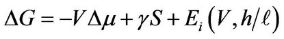 (1)
(1)
where ΔG—Gibbs free energy, V—nucleations volume, Δμ—thermodynamic driving force of crystallization, γ— the surface energy of the nucleus, S—nucleations surface, Ei—the internal energy nucleations, h—height of the nucleations, ℓ—cross-size of the nucleations.
The first variable of equation (1) defines the formation work of the volume nucleation, second—the work, necessary to create additional surface nucleations, third—the elastic energy of the nucleation.
In the case of homogeneous thin film, the energy is determined by first two variable of equation (1). At heteroepitaxial formations appears additional third of the elastic deformation variable due to growth of strained layers. At large mismatch of lattice parameters of the film and the substrate, the magnitude of this additional energy depends not only on the nucleations volume V, but also on its shape h/ℓ, also defines the transition from 2D to 3D formation [2,3].
Process formation of highly ordered self-organized MS from NCs-Si islets ensembles on the surface of monocrystal Si in the process of its long etching is described by equation (2)
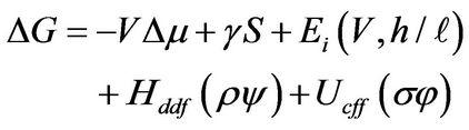 (2)
(2)
Parameters of additional variables Ηddf(ρψ) and Ucff(σφ) in equation (2) depend on macroscopical experimental conditions—features of electrochemical systems with an internal source of current, including characteristics of electrodes and cell parameters.
The equation (2) represents not only to the self-organizing processes occurring at nanostructuring with help electrochemical etching, but also the self-organizing processes in the conditions of “soft” impact. Also consideration of these forces can give new approaches to understanding of the nature of self-organizing processes at nanostructuring and development of new methods of NCs formation.
For example, the case the epitaxial growth of nanocrystals will be described by the equation (3)
 (3)
(3)
This equation (3) takes into account the additional role of defectively-deformative forces (Ηddf(ρψ) of ordering of PDs, which forming in conditions of “soft” impact at the epitaxial growth of NCs with different views of external impacts. Therefore, in equation (1) describing the mechanism of the epitaxial growth of islets NCs, we suggest to add the additional variable (Ηddf(ρψ) [6,13-15], which plays an important role in processes of epitaxial growth and self-organization of NCs islets.
4.5. The Nature of Cracks Occurring at the Electrochemical Etching of p-Si (100)
The nature of cracks on silicon ledges (figure 6) at long-term electrochemical etching of p-Si (100) in the EISC is defined by impact of defectively-deformative forces [6,13-15], arising at the space-temporal ordering of PDs. This ordering of PDs is determined by the conditions of their occurrence, which can be both “soft” and “hard”. “soft” conditions occurrence of PDs means the low-energetical laser, electron and ion irradiation. This “soft” impact induces the formation of close pairs Frenkel, interstitial (I) and vacancy (V), by breaking the chemical bonds of atoms in a crystal. A close pairs Frenkel’ can “collapse” with each other or to migrate individually on the various sinks. At this, because of differences in migration rate of I and V occurs their spatial and temporal separation, as in the case of electrochemical etching. As a result, an elastic defectively-deformative field is formed [6], which contributes to their self-organization.
The conditions of “hard” (high-energy, high-dose) impacts form nonequilibrium, complex defects, such as disordering, clusters, blistering effects, the formation of gas bubbles, peeling, swelling, blistering, etc., not considered. As in these cases there are other features of the formation of cracks and damage.
It is known, that the formation and growth of cracks in elastic media starts with the formation of pores [30]. It is therefore interesting to consider the possibility of cracking in an elastic solid through pores formation and participation in it the PDs on the example of Si monocrystal electrochemical etching in EISC. Si is the more wellstudied material in terms of understanding the dynamics of the birth of the point defects and formation of pores. Moreover, the conditions of «soft» impacts well manifested in silicon are compared with the other materials-metal, plastic, glasses, etc. In such conditions, the “soft” etching of silicon are initially formed PDs-ISi and VSi, after this occurs their space-time ordering in the form of depressions and protrusions [6,13-15], according to the orientation of the crystal surface. In sites of congestions VSi form hollows, in sites of congestions ISi form ledges. In hollows centers of pore formation arise. The congestions ISi initially leads to the formation of ledges and then at prolonged etching to cracks on them along certain crystallographic orientations.
Analogical spatial separation of the vacancy-interstitial clusters that form the wave relief of surface , as depresssions and protrusions, were observed in situ Si irradiated by electrons (1 MeV) in the high-voltage electron microscope [31]. It has been shown, that the predominant interaction of VSi with the crystal surface creates the energy barrier for mutual recombination of ISi and VSi. In these conditions, runoff of VSi to the surface provides accumulation of ISi in the surface region of the crystal. The dominance of interstitial defects determined is like oversaturation ISi, arising due to the inequality of the diffusion coefficients of vacancies kV and interstitial kI, kV << kI.
It should be noted that the dependence of the depth of the interstitial clusters in the surface region from the thickness of the oxide on the surface of the Si during irradiation with high-energy (1 MeV) electrons [31]. Shown that at oxide thickness of 1 nm, the zone of ISi runoff is 300 nm, and at the thickness oxide of 15 - 30 nm, the zone of ISi runoff decreased to 15 - 30 nm. The similar phenomena observed in the case of electrochemical etching of Si in HF. The process of etching of Si in HF occurs through dissolution of SiO2, and thus, excluded the influence of silicon oxide on the depth of the zone runoff for ISi. And so perhaps the long range of ISi (interstitial clusters) in the surface region, as noted in [31].
The condition of the “soft” impact can be realized at low-energetical effects—laser, electron, ion irradiation when the formation of the wave surface relief of the crystal are observed on account of the spatial and temporal distribution of the PDs [6]. When at achieving the critical concentration of the accumulation of PDs in elastic crystals the cracks are formed. As an example, one can refer to a well-known concept as “fatigue strength,” when long-time exposure forms the cracks. Also the “fatigue strength,” formation cracking, and material destruction are observed at prolonged mechanical influences. This is possible under the optimal conditions and with the thermal, chemical, and other influences. All these give basics to conclude that the formation of cracks is of the common nature. It is determined by the initial stage of defect formation. Namely, the “soft” condition of PDs formation, when possibly space-temporal separation of ISi and VSi [32].
5. Conclusions
The spontaneous self-formation of 3D-islets of Si-NCs at the long anodic etching of p-Si (100) in the electrolyte with an internal source of the current occurs due to the relaxation of elastic stress of the secondary porous layer.
Morphology of MS por-Si, period of 3D-islets Si-NCs por-Si, their dimensions are defined by the joint actions of the defectively-deformative forces of ordering PDs and capillary-fluctuation forces are generated by IF electrolyte/Si-NCs por-Si/c-Si.
Self-organization mechanism of MS por-Si at long anodic etching of p-Si (100) in the electrolyte with an internal current source is described by equation of the mechanism Stranski-Krastanov with additional variables of the defectively-deformative forces for ordered of point defects and capillary-fluctuation forces, generated on the IF electrolyte/semiconductor.
Conditions for the manifestation of these forces are determined by macroscopic conditions of the experiment, including the characteristics of the electrodes and the cell parameters, when appears the conditions of “soft” impacts.
Nature of cracks at long-term electrochemical etching of p-Si (100) is determined by the processes of the spatial-temporal ordering of point defects in conditions of “soft” impact.
It is concluded about the common nature of the radiation and non-radiation cracks, emerging in condition of “soft” impact. Nature of cracks is determined by the formation of spatial-temporal ordering of the PDs.
REFERENCES
- K. B. Tynyshtykbaev, Yu A. Ryabikin, S. J. Tokmoldin and R. B. Vermenichev, “Surface of the Porous Silicon Received in Electrolyte with an Internal Source of a Current,” Materials Today, Vol. 13, No. 11, 2010, p. 3. http://digital.materialstoday.com//launch.aspx?eid=81d97740-a77f-4f0b-a164-628df6b04425
- N. N. Ledentsov, V. M. Ustinov, S. V. Ivanov, B. Ya. Mel’tser, M. V. Maksimov, P. S. Kop’ev, D. Bimberg and Zh. I. Alferov, “Ordered Quantum-Dot Arrays in Semiconducting Matrices,” Physics-Uspekhi, Vol. 39, No. 4, 1996, pp. 393-398. http://iopscience.iop.org/1063-7869/39/4/A04
- S. A. Kukushkin and A. V. Osipov, “Thin Film Condensation Processes,” Physics-Uspekhi, Vol. 4, No. 4, 1998, pp. 983-1014. http://iopscience.iop.org/1063-7869/41/10/R02
- K. B. Tynyshtykbaev, Yu. A. Ryabikin, S. Zh. Tokmoldin, T. Aytmukan, B. A. Rakymetov and R. B. Vermenichev, “The Morphology of Porous Silicon at Long Anodic Etching in Electrolyte with Internal Current Source,” Technical Physics Letters, Vol. 36, No. 6, 2010, pp. 538-540. doi:10.1134/S1063785010060155
- K. B. Tynyshtykbaev, Yu. A. Ryabikin, S. J. Tokmoldin, B. A. Rakymetov and T. Aytmukan, “Dynamics of the Formation of the Mosaic Structure of Porous Silicon at Long Anodic Etching in Electrolytes with Internal Power Source,” Physics of the Solid State, Vol. 53, No. 8, 2011, pp. 1575-1580. doi:10.1134/S1063783411080312
- V. I. Emelyanov, “Self-Organization of Ordered Ensembles of Nanoparticles upon Laser-Controlled Deposition of Atoms,” Quantum Electronics, Vol. 36, No. 6, 2006, pp. 489-507. doi:10.1070/QE2006v036n06ABEH013189
- A. Valance, “Porous Silicon Formation: Stability Analysis of the Silicon-Electrolyte Interface,” Physical Review, Vol. 52, No. 11, 1995, pp. 8323-8336. doi:10.1103/PhysRevB.52.8323
- A. V. Klimov and A. I. Grigor’ev, “On nonlinear Periodic Capillary-Fluctuation Wave Flow in a Thin Liquid Film on a Solid Substrate,” Technical Physics, Vol. 54, No. 10, 2009, pp. 1415-1422. doi:10.1134/S106378420910003X
- D. N. Goryachev, L. V. Belyakov and O. M. Sreseli, “The Electrolytic Process for the Preparation of Porous Silicon Using an Internal Current Source,” Semiconductors, Vol. 37, No. 4, 2003, pp. 494-498. doi:10.1134/1.1568472
- R. L. Smith and S. D. Collins, “Porous Silicon Formation Mechanisms,” Journal of Applied Physics, Vol. 71, No. 8, 1992, pp. 1-22. doi:10.1063/1.350839
- K. N. El’cov, V. A. Karavanskii and V. V. Martynov, “Modification of Porous Silicon in Ultrahigh Vacuum and the Contribution of Graphite Nanocrystals Photoluminescence,” JETP, Vol. 63, No. 2, 1996, pp. 106-111. http://link.springer.com/article/10.1134%2F1.566989
- A. S. Len’shin, V. M. Kashkarov, S. Yu. Turishchev, M. S. Smirnov and E. P. Domashevskaya, “Effect of Natural Aging on Photoluminescence of Porous Silicon,” Technical Physics Letters, Vol. 37, No. 9, 2011, pp. 789-792. doi:10.1134/S1063785011090124
- V. I. Emelyanov, K. I. Eremin and V. V. Starkov, “Defect-Deformation Mechanism of Spontaneous Nucleation of an Ensemble of Pores in Solids and Its Experimental Verification,” Quantum Electronics, Vol. 32, No. 6, 2002, pp. 473-475. doi:10.1070/QE2002v032n06ABEH002225
- V. I. Emelyanov, K. I. Eremin, V. V. Starkov and E. Yu. Gavrilin, “Quasi One-Dimensional Distribution of Macropores during the Anodic Etching of Uniaxial Strained Silicon Wafers,” Technical Physics Letters, Vol. 29, No. 6, 2003, pp. 19-25. http://link.springer.com/content/pdf/10.1134%2F1.1565641.pdf
- V. I. Emelyanov, V. V. Igumnov and V. V. Starkov, “The Dynamics of Self-Organization of Hexagonal Pore Arrays during Anodic Etching and Oxidation of Semiconductors and Metals,” Technical Physics Letters, Vol. 30, No. 10, 2004, pp. 83-88. http://link.springer.com/article/10.1134%2F1.1760879
- A. F. Andreev and A. Ya. Parshin, “Equilibrium Shape and Oscillations of the Surface of Quantum Crystals,” JETP, Vol. 48, No. 4, 1978, pp. 1511-1516. http://www.jetp.ac.ru/cgi-bin/dn/e_048_04_0763.pdf
- V. I. Marchenko and A. Ya. Parshin, “Elastic Properties of Crystal Surfaces,” JETP, Vol. 52, No. 1, 1980, pp. 157-160. http://www.jetp.ac.ru/cgi-bin/dn/e_052_01_0129.pdf
- V. I. Marchenko, “Possible Structures and Phase Transitions on the Surface of Crystals,” JETP, Vol. 33, No. 8, 1981, pp. 381-383. http://ftp.kapitza.ras.ru/people/mar/JETPL81.PDF
- A. F. Andreev and Yu. A. Kosevich, “Capillary Phenomena in the Theory of Elasticity,” JETP, Vol. 81, No. 4, 1981, pp. 1435-1443. http://prb.aps.org/abstract/PRB/v52/i11/p8323_1
- O. P. Pchelyakov, Yu. B. Bolkhovityanov, A. V. Dvurechenskii, L. V. Sokolov, A. I. Nikiforov, A. I. Yakimov and B. Voigtländer, “Silicon-Germanium Nanostructures with Quantum Dots: Formation Mechanisms and Electricalproperties,” Semiconductors, Vol. 34, No. 11, 2000, pp. 1229-1247. doi:10.1134/1.1325416
- V. I. Emelyanov and V. V. Starkov, “Nonlinear Dynamics of Self-Organization of Hexagonal Ensembles Since the Oxidation and Etching of Metals and Semiconductors,” Journal of Surface Investigation. X-Ray, Synchrotron and Neutron Techniques, Vol. 36, No. 11, 2006, pp. 53-68.
- Yu. B. Bolkhovityanov, V. I. Yudaev and A. K. Gutakovsky, “The Initial Stages of Heteroepitaxy from the Liquid Phase at a Low Misfit: InGaAsP on GaAs,” Thin Solid Films, Vol. 137, No. 1, 1986, pp. 111-121. doi:10.1016/0040-6090(86)90199-9
- D. F. Timokhov and F. P. Timokhov, “The Influence of the Crystallographic Orientation of the Silicon to Form Silicon Nanoclusters during Anodic Electrochemical Etching,” Semiconductors, Vol. 43, No. 1, 2009, pp. 95-99. doi:10.1134/S1063782609010175
- D. J. Eaglesham, A. E. White, L. C. Feldman, N. Moriya, and D. C. Jacobson, “Equilibrium Shape of Si,” Physical Review Letters, Vol. 70, No. 1, 1993, pp. 1643-1646. doi:10.1103/PhysRevLett.70.1643
- A. A. Shklyaev and M. Ichikawa, “Extremely Dense Arrays of Germanium and Silicon Nanostructures,” PhysicsUspekhi, Vol. 51, No. 2, 2008, pp. 133-161. http://iopscience.iop.org/1063-7869/51/2/R02
- L. V. Belyakov, D. N. Goryachev and O. M. Sreseli, “The Role of Singlet Oxygen in the Formation of Nanoporous Silicon,” Semiconductors, Vol. 41, No. 12, 2007, pp. 1473- 1476. doi:10.1134/S1063782607120135
- V. F. Kiselev and O. V. Krylov, “Electronic Phenomena in Adsorption and Catalysis on Semiconductors and Dielectrics,” Nauka, Moscow, 1979. http://www.amazon.com/dp/3642830226
- W. W. Mullins and R. F. Sekerka, “Stability of a Planar Interface During Solidification of a Dilute Binary Alloy,” Journal of Applied Physics, Vol. 35, No. 11, 1964, pp. 444-451. doi:10.1063/1.1713333
- N. N. Gerasimenko, K. K. Dzhamanbalin and N. A. Medetov, “Self-Assembled Nano-Structures on the Surface and in the Bulk Semiconductor,” Alem, Almaty, 2002.
- P. G. Cheremskoy, V. P. Betehtin and V. V. Slezov, “The Pores in the Solid State,” Energoatomizdat, Moscow, 1990.
- L. I. Fedina and A. L. Aseev, “Atomic Mechanisms of Clustering of Intrinsic Point Defects in Si,” In: A. L. Aseev, Ed., Nanotechnology in Semiconductor Electronics, Sibirean Branch Russian Academy of Sciences, Novosibirsk, 2004, pp. 179-201. http://85.142.23.144/packages/mifi/5E6AE615-986F-4DE6-8BAB-1190A19D7E93/1.0.0.0/15.pdf
- K. B. Tynyshtykbaev, “Self-Organization of Highly Ordered Mosaic Structure of Porous Silicon at Long Anodic Etching of p-Type Silicon in the Electrolyte with Internal Current Source,” Proceeding of International Conference on Multimedia Technology (ICMT), Hangzhou, 26-28 July 2011, pp. 6528-6531. http://ieeexplore.ieee.org/xpl/login.jsp?tp=&arnumber=6002582&url=http%3A%2F%2Fieeexplore.ieee.org%2Fxpls%2Fabs_all.jsp%3Farnumber%3D6002582
NOTES
*This work was supported financially by the Ministry of Science and Education of Republic of Kazakhstan. Grant No 169/2013. We are also grateful Zaure Idrissova for the help in this work.
#Corresponding author.