Materials Sciences and Applications
Vol.3 No.4(2012), Article ID:18466,10 pages DOI:10.4236/msa.2012.34029
Modulus and Hardness Change of Silicon and Sapphire Substrates by TiC/VC Multilayer Coatings
![]()
1On Leave from Institut für Strukturphysik, Technische Universität Dresden, Dresden, Germany; 2Triebenberg Laboratory, Institut für Strukturphysik, Technische Universität Dresden, Dresden, Germany; 3Institut für Strukturphysik, Technische Universität Dresden, Dresden, Germany.
Email: *paufler@physik.tu-dresden.de
Received January 30th, 2012; revised February 27th, 2012; accepted March 28th, 2012
Keywords: TiC/VC@Si or Sapphire Multilayers; Superlattice Effect; X-Ray Absorption Spectrometry; Electron Microscopy
ABSTRACT
The nanohardness H of multilayer specimens TiC/VC@Si and TiC/VC@Sapphire prepared by Pulsed-Laser-Deposition is investigated to check the existence of a superlattice effect as known from TiN/VN multilayers. In the present work the multilayer period thickness l varies between 1.34 nm and 24.8 nm (total layer thickness t ≈ 200 nm). Unlike Young’s modulus E, H is enhanced, regardless of t, by covering Si as well as sapphire with a TiC/VC multilayer; the relative load carrying capacity being larger for Si. The maximum value of H obtained is 38 GPa for TiC/VC@Sapphire. It is observed for a multilayer thickness of l » 10 nm. Hardness of TiC/VC@Sapphire obeys, after annealing, a Hall-Petch relation H = 35.25 + 6.945 l–0.5 (H in GPa und l ³ 10 nm). From orientation dependent X-ray absorption fine structure and X-ray reflection records, short-range order and layer geometry are derived. These analyses reveal a continuous approach of interatomic distances Ti-C and V-C for deceasing multilayer periods. High-resolution transmission electron microscopy shows that multilayers are nanostructured, i.e., not only TiC/VC phase boundaries but also subgrains represent obstacles against plastic deformation. Dislocations play a major role as sources of internal stress and vehicles of plasticity.
1. Introduction
Both elastic modulus and hardness values of multilayer (MuL) thin films can exceed those of the single layers and of bulk objects. Multilayers or composition-modulated films may exhibit an increase of the elastic moduli (“supermodulus effect”) as a result of large coherency strains between the layers [1]. They are often higher than the values suggested by a simple rule of mixture between layer materials.
Unexpected values of hardness H have attracted more attention. Material with H > 40 GPa is considered superhard [2]. Getting ahead of this value became a major goal of materials research. The appearance of a hardness maximum, Hmax, of a MuL@substrate system as a function of MuL period thickness, λ, was designated “superlattice hardening” [3,4]. Single crystalline TiN/VN MuLs on MgO substrate represented an early example. For λ = 5.2 nm a maximum hardness of Hmax = 54.5 GPa [5] occurred.
Most models of superlattice hardening at nanoscopic scale refer to impeding of dislocation motion [6,7], because dislocations are the main vehicles of strain. Models differ in the kind of major obstacles. Also alternative mechanisms have been considered, like, for example, extension of microcracks [8].
So far, a wide variety of MuL coatings have been studied to improve the resistance of various metallic or nonmetallic bulk material (cf., e.g., Abadias et al. [9]). The aim of the present work was to study the nanohardness of TiC/VC MuLs on silicon (point symmetry group ) and sapphire (
 ) substrates, respectively. These carbides have been less frequently paid attention to. Strafford [10] quoted Vickers hardness values for TiC (27.1 - 40.7) GPa and VC (18.6 - 27.9) GPa, respectively. Phani et al. [11] found the nanohardness of 800 - 900 nm TiC films to be in the range 25 - 30 GPa. Moreover, referring to their complete solid solubility thanks to the same NaCl structure type and similar lattice parameters (TiC 0.43176 nm, VC 0.41599 nm) superlattice hardening could be expected.
The present study focuses upon substrates silicon and sapphire. Both materials have become attractive as part of electronic devices. The following nanohardness values H have been reported for single crystalline silicon: H = 13 GPa for (100) and 16 GPa for (111) surfaces [12]. (0001) surfaces of sapphire exhibited H = (29.1 ± 0.1) GPa [13] at a depth of 200 nm. Improving their resistance against indentation, scratching and wear is a goal of economic importance. Preliminary work on TiC/VC@ Si and sapphire has been communicated elsewhere [14]. Special attention will be paid to the structure at nanoscale and its influence upon hardness.
2. Experimental
2.1. Preparation
TiC/VC MuLs (area 2 × 3 cm2) were prepared on sapphire (012) and silicon (001) single crystals at room temperature in vacuum (5 × 10⁻⁶ Pa) by pulsed laser deposition (PLD) employing a Nd-YAG-Laser (Spectra Physics, GCR 5 - 20). The hardness of TiC layers can be increased essentially from about 20 to 44 GPa when applying PLD instead of magnetron sputtering [15]. Preliminary films obtained by us with the aid of solid-state reaction of PLD C-Ti-C-V MuLs exhibited strong composition gradients. Therefore, rod-shaped TiC and VC targets (hot-pressed powders) were preferred for PLD to ensure transfer of stoichiometric composition to the films. Laser parameters were chosen such that a gentle congruent ablation was going on: wavelength 355 nm, pulse duration 8 ns, pulse frequency 20 Hz, pulse energy 150 mJ, distance target-substrate 175 mm. Results of elemental analysis are given in Table 1. No contamination of the MuL with oxygen could be detected by electron probe microanalysis. X-ray reflectometry showed, however, that an oxide layer of about 1 - 2 nm thickness had formed on top of the stack after removing the sample from vacuum. An influence of this thin oxide upon properties of the stack could not be observed.
The total thickness t of the double layer package intended was 200 nm, corresponding to a range of specimens coated by 5 ∙∙∙ 100 double layers. 7 and 21 specimens were prepared on silicon and sapphire substrates, respectively. Moreover, single layers of TiC and VC on Si and Al2O3 substrates were also provided for comparison.
2.2. Structural Characterization
Structural characterization of MuLs was performed using X-ray reflectometry (XR), wide-angle X-ray scattering (WAXS) and extended X-ray absorption fine structure study (EXAFS) [16]. For details of the experimental procedure cf. [17]. Figure 1 shows XR curves of selected
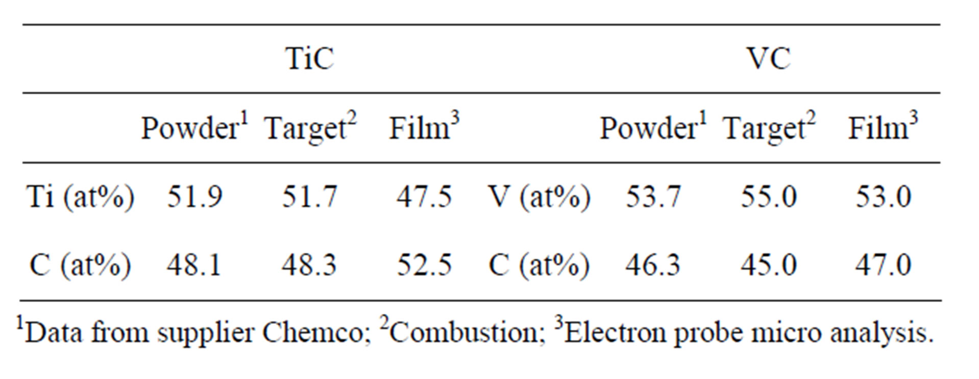
Table 1. Chemical composition of target and films when exploiting compound targets.
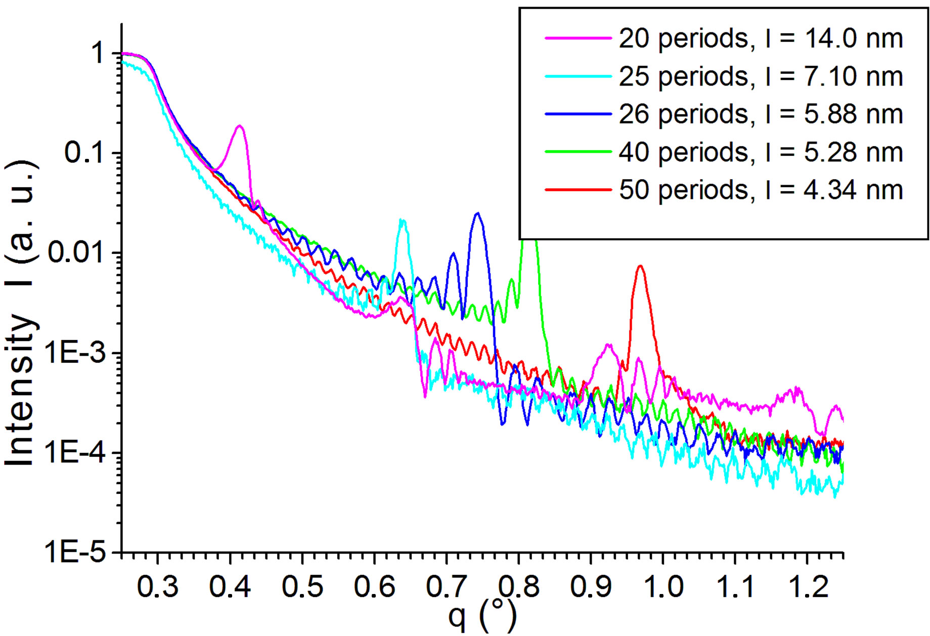
Figure 1. Experimental XR data of reflected intensity versus diffraction angle q = θ of TiC/VC multilayers on (012) sapphire substrate for selected multilayer periods l = 1. The appearance of the second Bragg reflection for the 2θ- period multilayer indicates a deviation from the planned thickness ratio TiC:VC = 1:1.
MuLs on sapphire. The position of the first Bragg reflection is shifted as a function of superlattice parameter λ. The roughness of all samples amounted to 0.5 nm. Additionally, two samples (50 and 40 periods) were annealed (pressure p < 1000 - 600 Pa, 5 hours, 500˚C) to check the stability of the system. No change of the thickness but doubling of the roughness occurred due to this thermal treatment. Examples of XR analysis are summarized in Table 2.
The crystal structure of MuLs was refined by means of an X-ray diffractometer Siemens D5000 with a secondary monochromator tuned to CuKα radiation making use of the asymmetric approach method (FPA) of the Rietveld program TOPAS 2.0. This enabled refinement of lattice parameters and crystallite sizes taking the diffracttometer device function into account. 220 reflection could be observed only, which exhibits a half width (0.55˚) smaller than the MuL Bragg reflections 220 of TiC/VC and of single layer TiC (Figure 2). Quantitative results are given in Table 3. For MuLs with smaller periods, lattice parameters could not be obtained because of poor resolution.
Figure 3 shows that, due to annealing, 220 peaks of TiC and VC sublayers were shifted to higher Bragg angles and their half widths decreased. That means cubic
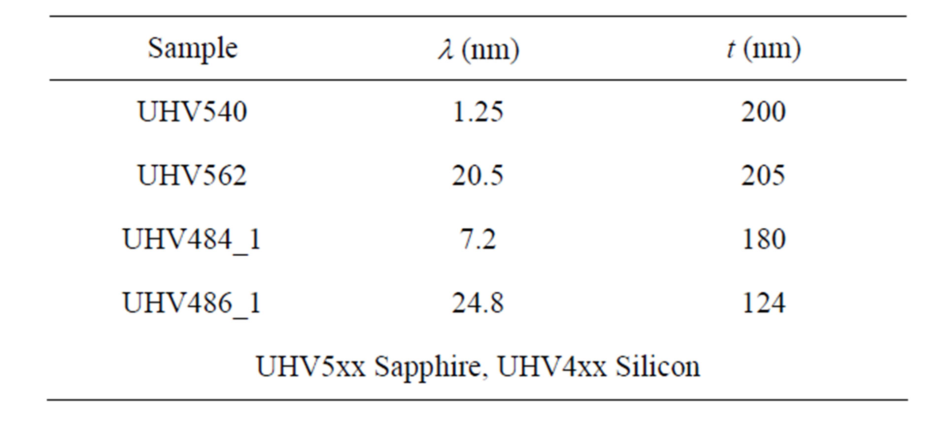
Table 2. Geometry of selected samples.
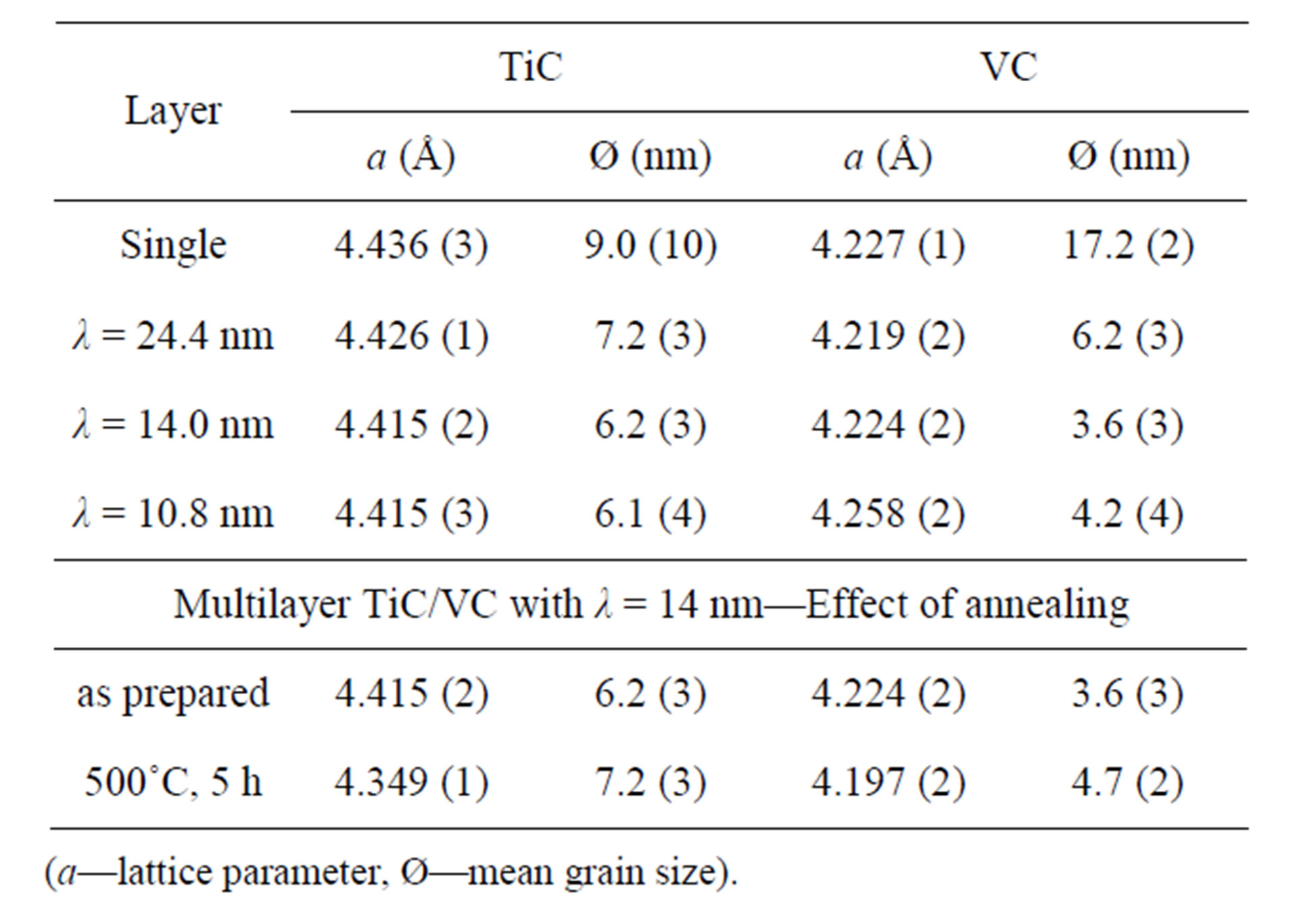
Table 3. Results of TOPAS analysis of TiC/VC@sapphire and influence of annealing (a lattice parameter, Ø grain diameter).
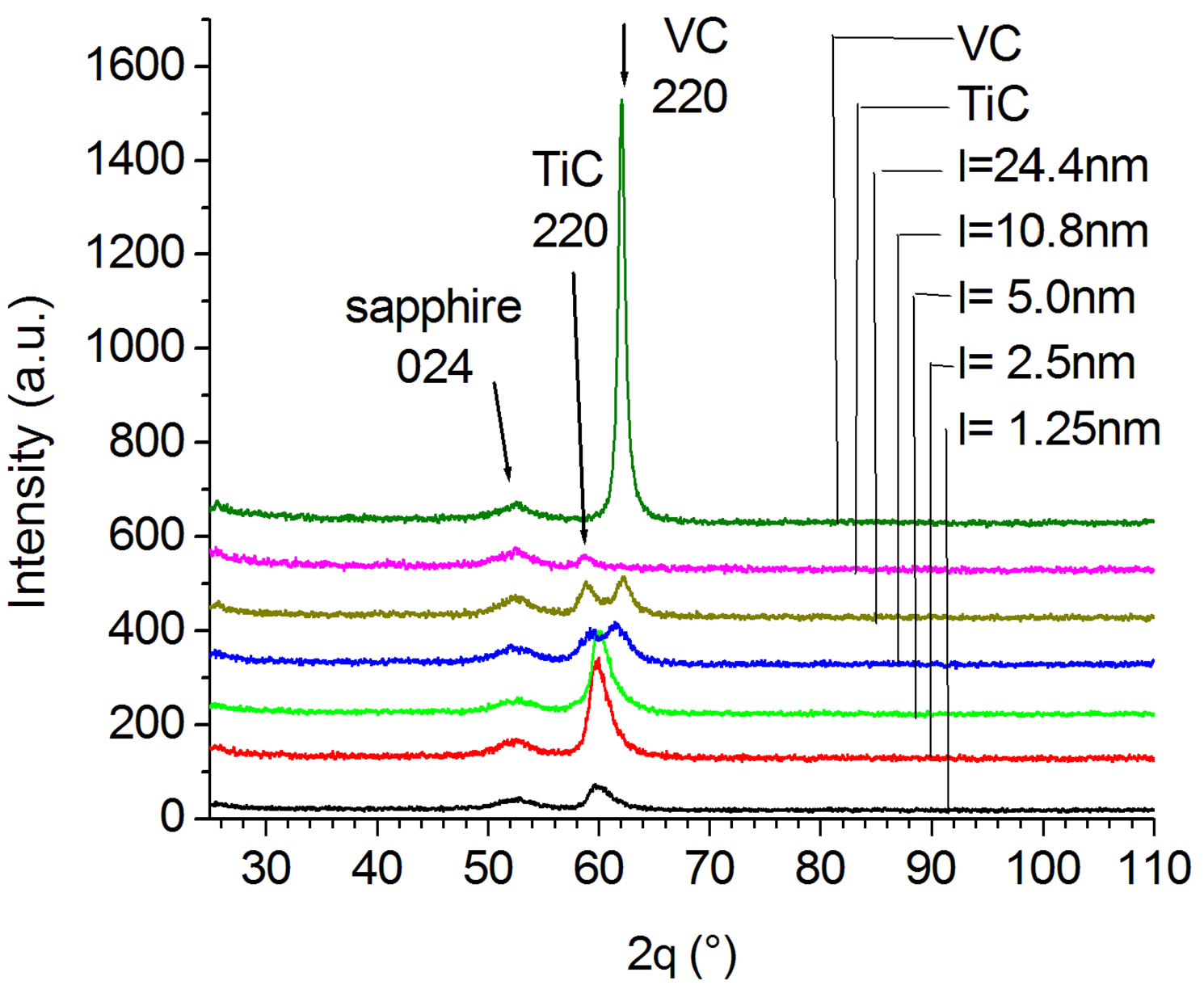
Figure 2. Comparison of the WAXS pattern vs diffraction angle 2q ≡ 2q of single layer TiC, VC and TiC/VC-MuL films on sapphire (012) with different MuL periods l ≡ l.
lattice parameters of both phases decreased and subgrain sizes increased slightly. Numeric data are presented in Table 3. Grain sizes Ø are of the same order as layer thicknesses. Also, Ø is decreasing when layers get thinner. This will be of importance for layer hardness.
Helming [18] has determined the texture of both single layers and a MuL utilizing an area detector [19]. The texture of single VC was found the most pronounced (half width < 10˚). (110) planes of VC were almost parallel to the substrate normal. While (110) planes of single TiC deviated most, the MuL system seemed to be an average of both single layers. Note that the slip system of TiC at room temperature is {110} <1 - 10> changing at elevated temperatures to {111} <1 - 10>. Normal stress applied at room temperature upon the MuL would thus give rise to vanishing shear stress along the slip planes thus increasing the resistance against deformation.
For an assessment of structure gradients inside MuLs, measurements of short range order were performed employing fluorescence EXAFS experiments (Figure 4). They were carried out at the beam line E4 at HASYLAB using a Si 111 double crystal monochromator, a nitrogen filled ionization chamber and an energy dispersive Ge detector (step width 0.5 eV around the edges, sampling time 2 - 9 s) [20]. Fourier transform of the EXAFS function yielded a measure of the radial distribution of atoms near the fluorescent species. Figure 5 shows an example. Fitting a model function to experimental data yielded interatomic distances and coordination numbers. A special feature of the present experimental set-up was a specimen
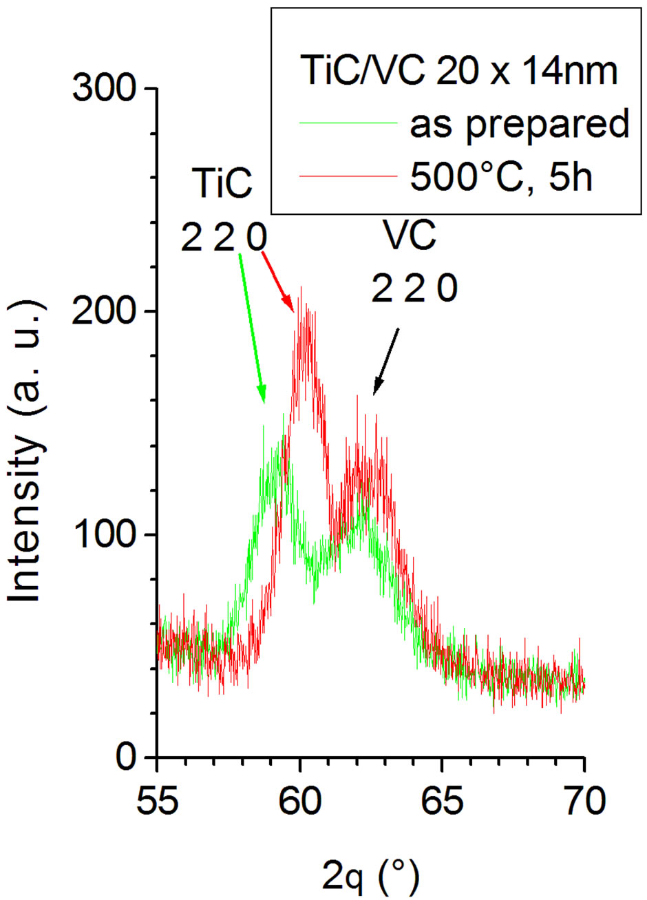
Figure 3. Pattern of WAXS intensity versus diffraction angle 2q taken from a TiC/VC@sapphire sample prior to and after annealing (500˚C, 5 hours).
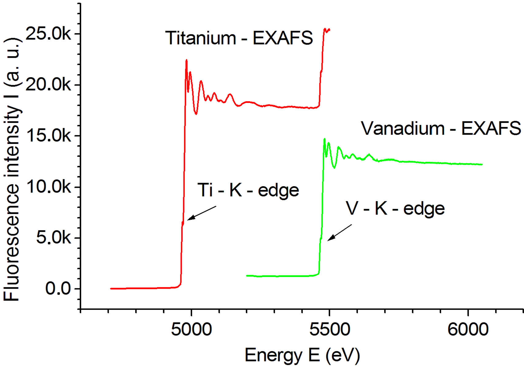
Figure 4. Fluorescence intensity versus photon energy near Titanium and Vanadium K absorption edges of a TiC/VC multilayer UHV 502 (λ = 4.34 nm) sample.
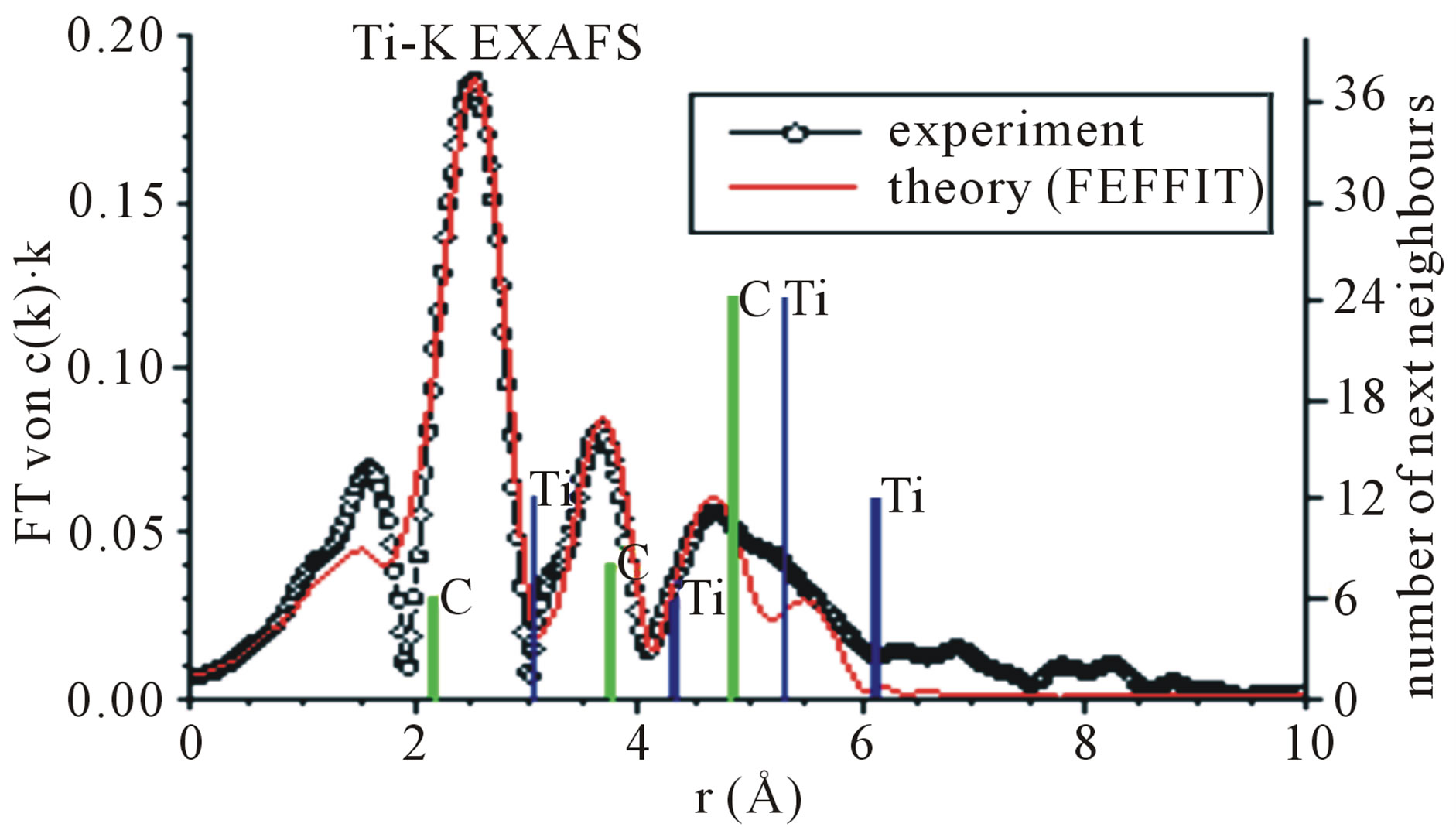
Figure 5. Fourier transform of the EXAFS function versus the radius vector r centered at a Ti atom. The right ordinate indicates the number of neighbors at distance r. Distances and numbers of C and Ti neighbors calculated from the crystal unit cell (lattice parameter a = 4.328 Å) are marked by green and blue bars. Note that the first maximum at about 1.5 Å is virtual (Specimen UHV 502).
holder, enabling the orientation of the linearly polarized synchrotron radiation to be varied. So, the short-range order parallel to the multilayer (“in-plane”) and perpendicular to it (“off-plane”) could be distinguished. Figure 6" target="_self"> Figure 6 indicates the geometry of the experiment schematically. Arrows are parallel to the polarization vector of the synchrotron radiation. If the specimen is “off-plane” oriented, the neighborhood of the fluorescent metal atoms is probed mainly perpendicular to the layer, in the “inplane” case mainly parallel to it. Experimental data of orientation dependent nearest-neighbor distances of each multilayer sample were taken to identify a cubic lattice parameter parallel and perpendicular to the layer.
Results in Figure 7 show that lattice parameters of NaCl-type compounds TiC (bulk 4.328 Å) and VC (bulk 4.165 Å) approached one another for in-plane and out-ofplane values separately, when the double layer period λ was decreasing. This gives rise to tensile stress in VC and to compressive stress in TiC along the interface. There is no cubic symmetry whatever λ may be prior to annealing. The effect of annealing at 500˚C is demonstrated for very small and very large MuL thicknesses: in the former case, in-plane distances of both VC and TiC cells were increasing compared to the pre-annealing value, at the same time approaching each other. Correspondingly, out-of-plane spacings were decreasing. For large double layer periods in-plane and out-of-plane distances of VC become equal after annealing, i.e., the influence of epitaxial strain is negligible. TiC could not be determined. Decreasing the double layer thickness λ of the NaCl-type compounds TiC and VC, lattice parameters of TiC (bulk 4.328 Å) and VC (4.17 Å) monolayers approach one another giving rise to tensile or compressive stress. For λ ~ 4 nm in-plane lattice parameters of TiC and VC become equal presumably due to strong epitaxial interaction. Single layers on sapphire > 20 nm
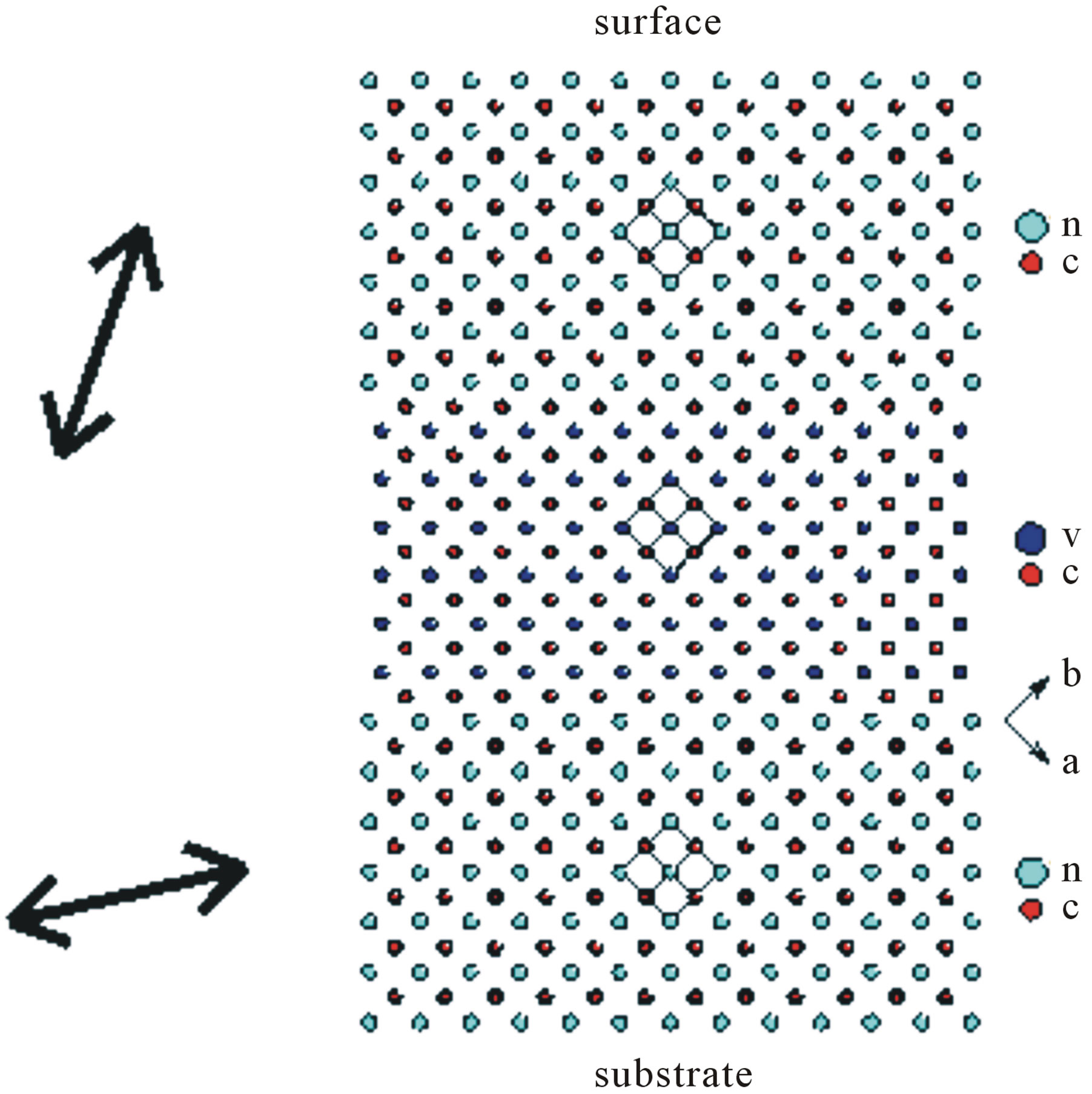
Figure 6. Schematic experimental set-up to take advantage of the linear polarization of synchrotron radiation. Due to geometrical constraints, orientations deviated from the exact in-plane (0˚) and out-of-plane (90˚) position.
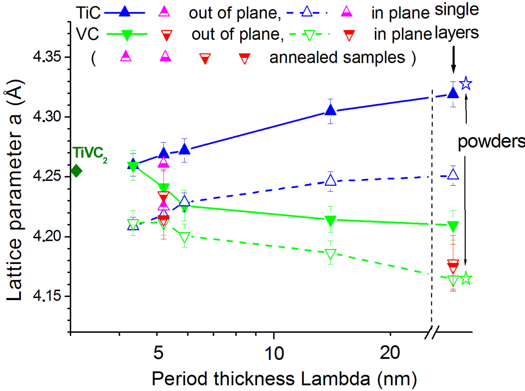
Figure 7. Lattice parameters a of TiC and VC parallel (inplane) and perpendicular (out-of-plane) to the multilayer surface as a function of multilayer period λ.
thick retain their tetrahedral cell. Cubic lattice parameters of powdered targets derived from powder diffraction are indicated for comparison. Investigating these identical specimens with the aid of transmission EXAFS at HASYLAB and analyzing them afterwards with codes FEFF6.01 und FEFFIT, yielded values smaller than obtained from powder diffraction. Therefrom a correction factor has been derived to adjust all EXAFS lattice parameters in Figure 7. This way the lattice parameter of solid solution TiVC2 appeared close to the out-of-plane figure of thin multilayers.
Provided that no intermixing of layers took place, strain can be used to estimate internal stress in the layer system. Assuming Young’s modulus for TiC or VC to be E » 300 GPa, the internal stress σ = Eε = EΔa/a is of the order of σ » ±3 GPa for Δa/a » 0.01.
2.3. Mechanical Characterization with the Aid of Nanoindentation
Nanoindentation (cf., e.g., [21]) was carried out under ambient conditions using a commercial nanoindenter (Hysitron Tribo Scope), which was attached to a scanning probe microscope (Nano Scope III Multimode). For experimental details we refer to [22]. Applying the procedure of [23], hardness H and the (reduced) Young’s modulus Er were evaluated. The Meyer hardness [24] H used here is defined as H = F(hc)/A(hc), where F is the applied force and A(hc) is the area of the indent projected onto the surface. hc is the true contact depth taking into account only that part of the penetration depth which is defined by an indenter-specimen contact.
Examples of load-penetration curves are displayed in Figure 8 for bulk trigonal sapphire prior to coating with TiC/VC multilayers. The first part of the hysteresis F(h) in Figure 8 can be fitted quite nicely on the basis of elastic deformation (Elastica [25]), where F ~ h1.53 holds, up to a critical force (or stress). Then plastic deformation starts (“pop-in”), whereby the nature of this process remains to be identified. Coating sapphire and silicon with TiC/VC MuLs changes the resistance against indentation. For a total layer thickness of about 200 nm the effect of MuLs is illustrated quantitatively in Figure 9. Note that the maximum penetration depth is smaller than the total layer thickness. Nevertheless, the substrate will be involved in the irreversible strain. The large pop-in of Figure 8 did not show-up again. Instead, smaller discontinuities occurred.
Hardness H of the MuL/substrate system obviously depends on the indentation depth h. We will come back to that and the way to attribute values of H in Figure 14
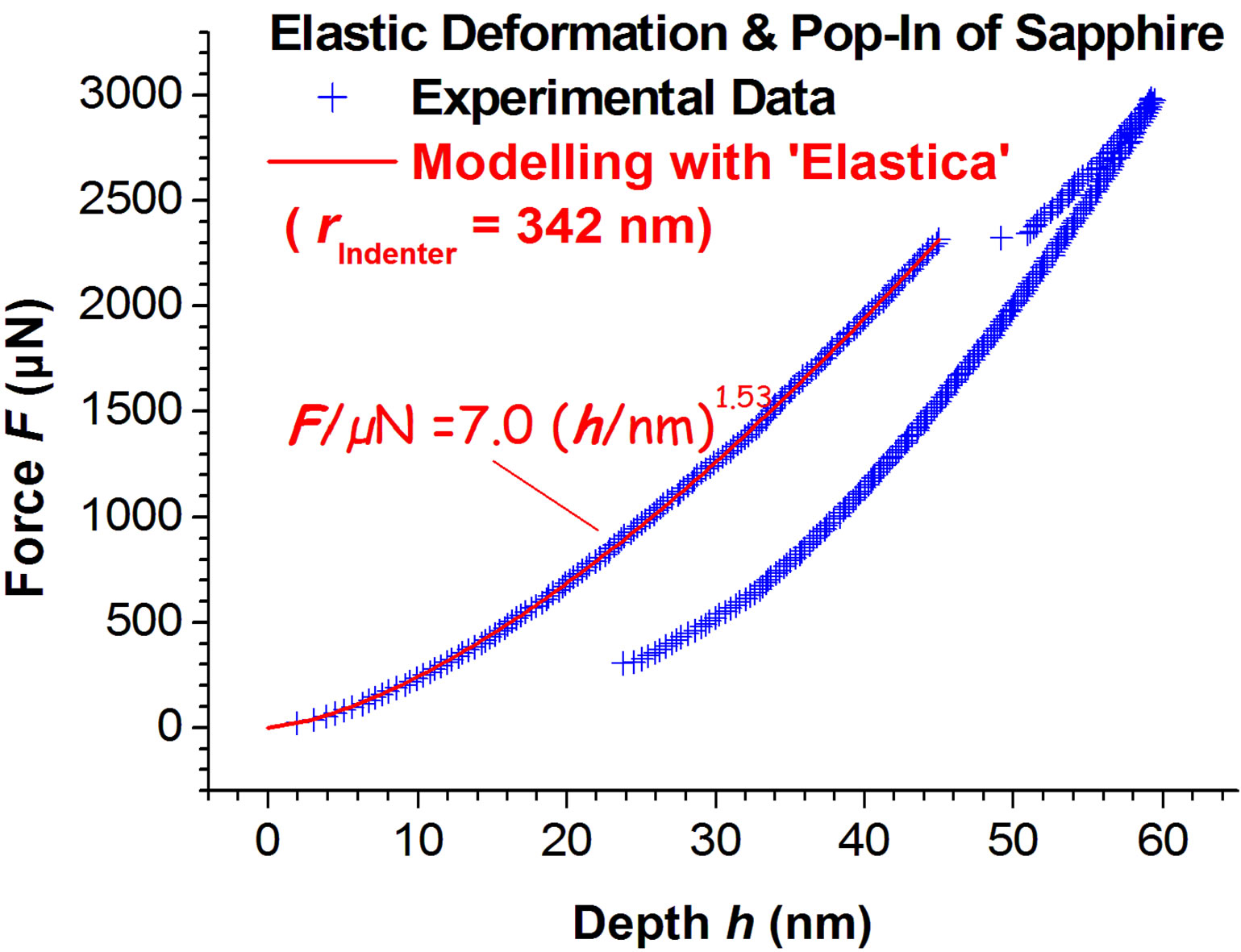
Figure 8. Force F versus indentation depth hysteresis for (01 - 12) sapphire at room temperature. “Pop-in” occurs at a normal force of about 2.3 mN. The tip radius of the indenter obtained as parameter of the fitting procedure amounted to 342 nm.
below.
Hardness H and reduced Young’s modulus Er have been evaluated from F(h) curves and plotted in Figures 10 and 11. Obviously, MuLs are enhancing H of Si as well as of sapphire at the penetration depths investigated (Figure 10). The H values of the MuLs achieved exceed those of bulk carbides and bulk substrates. If the depth of the indent approaches the total MuL thickness, the hardness gain due to the coating is diminished. Young’s modulus (see Figure 11) is practically unchanged by 200 nm coatings.
There is a small maximum of hardness as a function of layer period for samples with sapphire substrate (Figure 12). Data depend on the state of annealing. They prove hardest for a superlattice parameter λ » 10 nm. On this scale, MuLs of TiC/VC show a superlattice hardening effect.
2.4. Microstructure
For transmission electron microscopy (TEM) and High Resolution TEM (HRTEM) using a Philips microscope
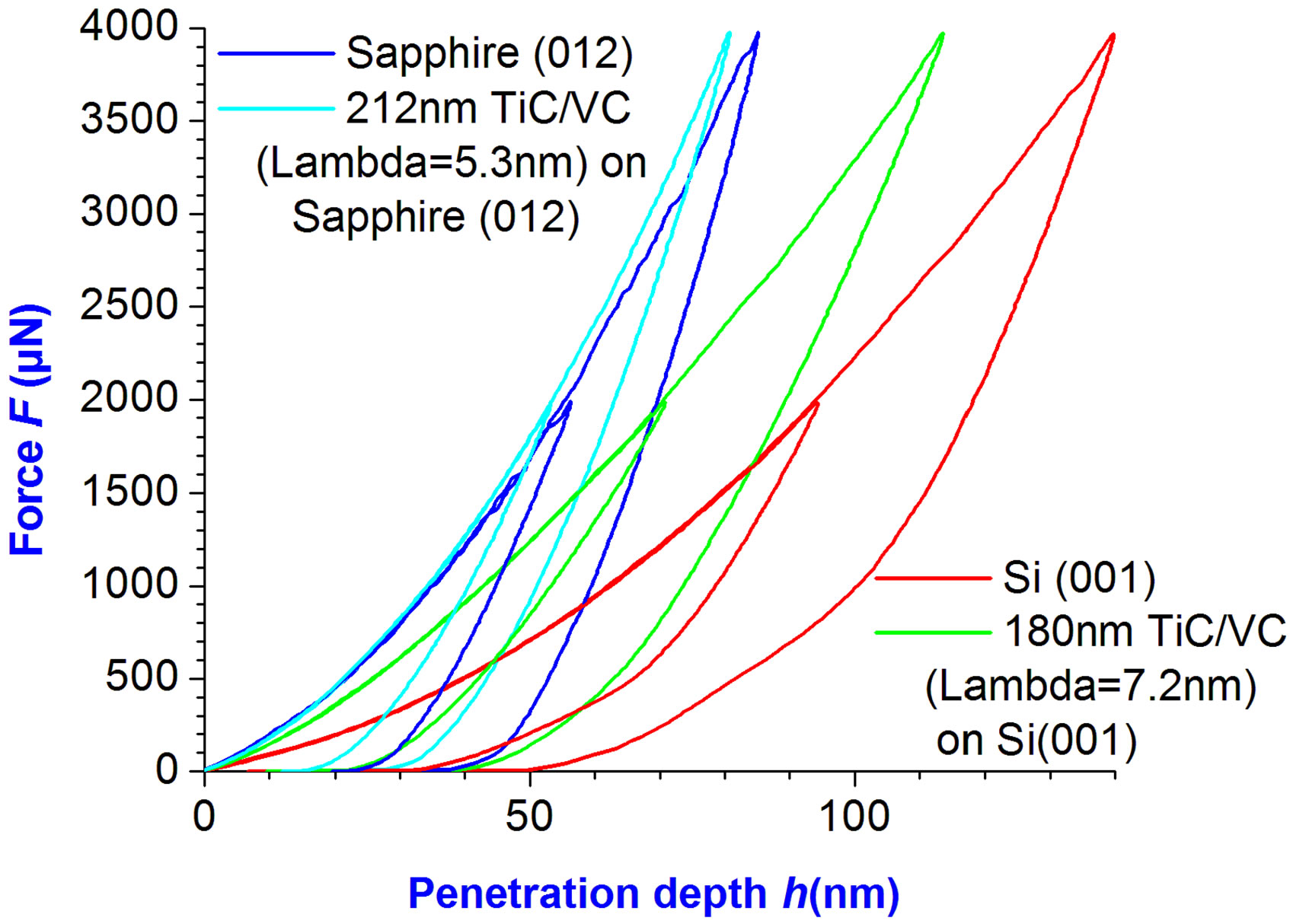
Figure 9. Force versus penetration depth of TiC/VC multilayers on Al2O3 (sapphire) and on Si. Data of uncoated sapphire and silicon are also given for comparison.
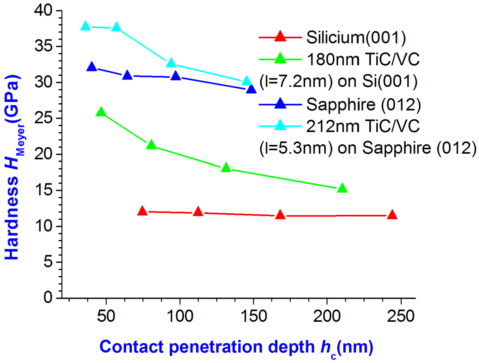
Figure 10. Impact of coating Si and Al2O3 with TiC/VC MuLs on hardness H at various penetration depths of the indenter.
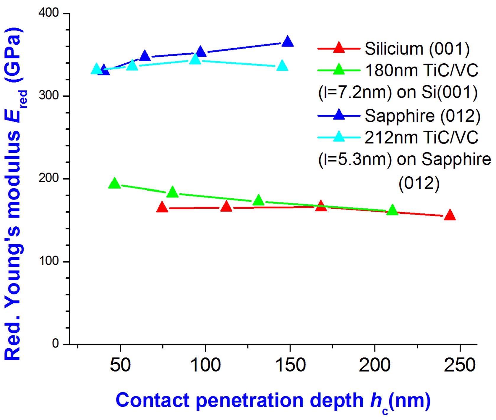
Figure 11. Impact of coating Si and Al2O3 with TiC/VC MuLs on Young’s modulus at various penetration depths of the indenter.
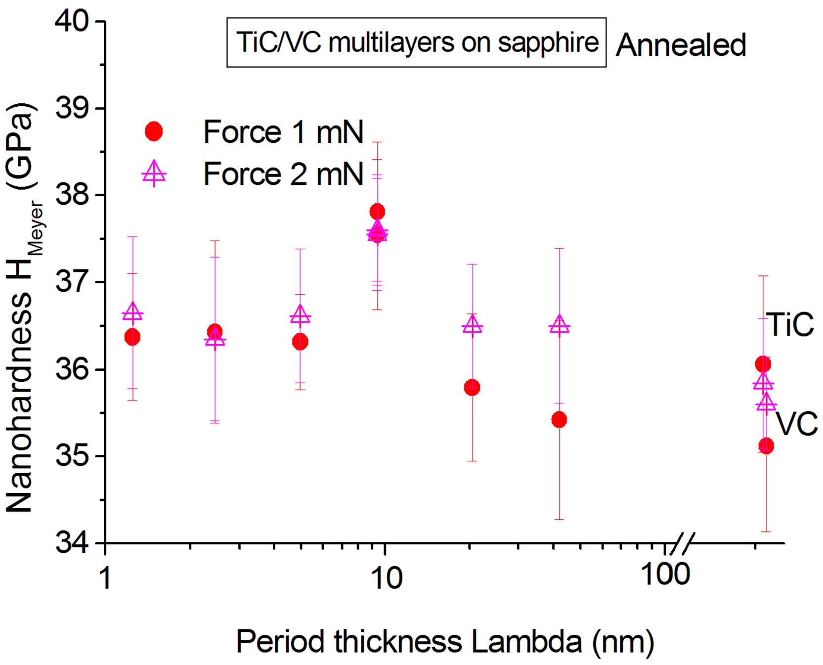
Figure 12. Hardness of TiC/VC@sapphire versus multilayer period λ after annealing. On the right hand side values of single layers TiC and VC on sapphire, respectively, are indicated. Small maximum for two distinct forces at about 10 nm.
CM30FEG, thin foils were prepared of as-received samples with orientations parallel and perpendicular to the surface of the MuL/substrate. Standard preparation techniques involving mechanical grinding, mechanical dimpling and ion milling to perforation have been applied.
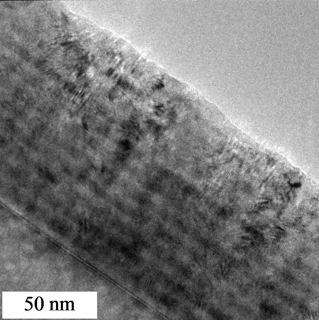
Figure 13 shows that nanograins have formed inside MuLs@sapphire. Secondly, columns of grains perpendicular to the layer plane have grown penetrating the layer interfaces. Subgrain and phase boundaries experienced sharpening during annealing. Mechanical properties measured with the aid of nanoindentation were Er = 313 GPa and 306 GPa as well as H = 37.2 GPa and 37.6 GPa prior to and after annealing.
3. Discussion
Two phenomena of the present results shall be recalled:
 (a)
(a)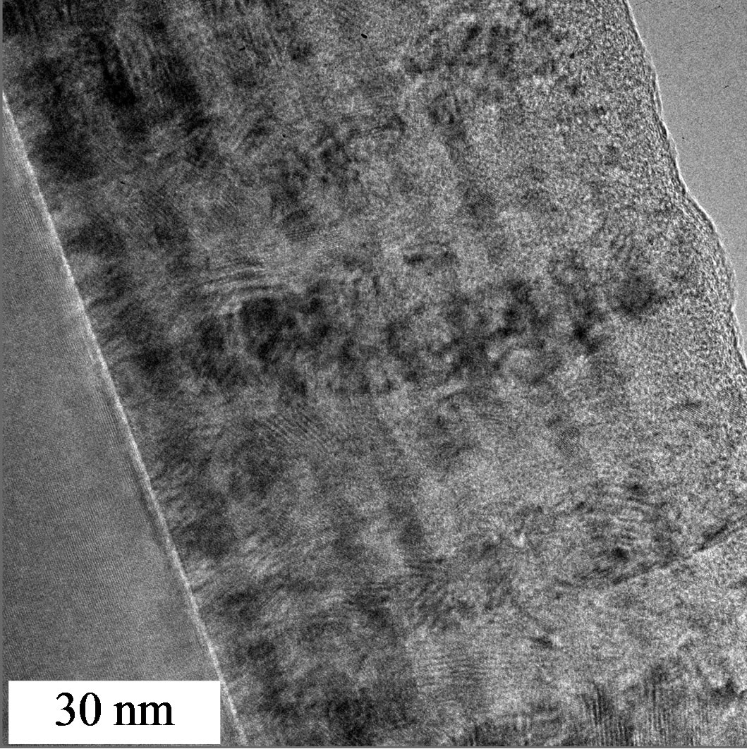 (b)
(b)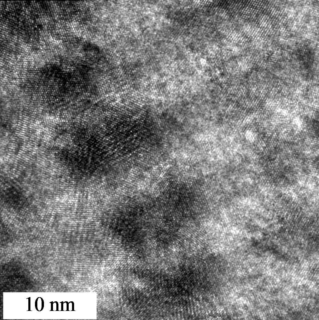 (c)
(c) (d)
(d)
Figure 13. HRTEM cross-sectional views (Philips CM30, field emission gun) of TiC/VC multilayers (10 periods) on sapphire prior to (a), (c) and after (b), (d) heat treatment (1 h, 500˚C). VC sublayers appear dark. Figures (c) and (d) reveal nanocrystalline and amorphous structure.
1) The general enhancement of hardness of substrates Si and Al2O3 due to coating with TiC/VC MuLs and 2) the enhancement of TiC/VC MuL hardness compared to TiC and VC bulk hardness. Since bulk H values of the carbides exceed those of substrates, the result 1) seems trivial. Looking more closely, the question arises what the load carrying capacity of a certain layer and the influence of the substrate deformation is like.
In Figure 14, taking advantage of the model of Korsunsky et al. [26], hardness values of substrate, Hs, and of the MuL, HMuL, were separated.
Authors decompose the total energy expenditure into the plastic work of deformation in the substrate and the deformation and fracture energy in the coating. The composite hardness, Hc, may be written Hc = Hs + (HMuL – Hs)/(1 + ß2[t/α]), where ß ≡ h/t denotes the indentation depth h normalized with respect to the MuL thickness t. α is a characteristic length of the order of t and hence t/α » const. This formulae takes the asymptotic behavior for ß ® ∞ (Hc = Hs + (α [Hf – Hs])/ß2t) and for ß ® 0 (Hc = HMuL) into account and hence covers the entire range of penetration depths. Numerical values of TiC/VC@Si are Hs = 13 GPa and HMuL = 32.9 GPa. Hs is in good agreement with the data of uncoated Si and HMuL is a plausible average of TiC and VC. Doing the same analysis with TiC/VC@ Al2O3 yielded Hs = 30 GPa and HMuL = 41.5 GPa.
The difference between HMuL = 32.9 GPa and HMuL = 41.5 GPa for the same MuL system on distinct substrates may be due to differences in microstructure or in interface structure or to both.
Turning now to the strengthening effect 2), we refer to Table 3 and Figure 13. Obviously, there is a structure beyond layering. Various nanoscaled mechanisms have been put forward to explain layer thickness dependent hardness. Misra et al. [7] proposed dislocation pile-ups (i.e. Hall-Petch behavior [27,28]) yielding the stress σ (λ) as σ ~ λ–0.5 for layer periods λ > 10 nm, bowing out of single dislocations inside a layer σ ~ (1/λ) lnλ for λ » 10 nm and interface crossing σ ~ λn for λ ≤ 1 nm. Plotting the present experimental H values for λ >10 nm is in support of a Hall-Petch mechanism (Figure 15). For λ < 10 nm H is almost constant. So, the behavior of the present thick MuLs is Hall-Petchlike. The slope dH/dλ of the H(λ–1/2) curve in Figure 15 amounts to 0.22 MN/m3/2. This is within the range of experimental findings for various metals (0.07 ∙∙∙ 1.7 MN/m3/2) given by Courtney [29]. However, a direct interpretation of MuL boundaries as rate-controlling dislocation obstacles seems less comprehensible when looking at Figure 13. Therefore, we adopt the view of Li [30] to avoid the pile-up model, i.e., we consider rather the empirical relationship λ ~ 1/ρ between obstacle spacing or grain size λ and dislocation density ρ. Then the increase of H (for λ > 10 nm) appears
Figure 14. Analysis of the composite hardness TiC/VC@Si according to Korsunsky et al. [26]. Hf ≡ HMuL.

Figure 15. Meyer hardness H of TiC/VC MuLs on sapphire versus MuL layer thickness λ. Data refer to values λ ³ 10 nm. Linear fit yields H = 35.25 + 6.945 xλ–1/2 (H values determined at maximum load 2 mN).
as consequence of an increase of average dislocation density according to H ~ ρ1/2. For MuLs with λ ® 0, H is approaching a level corresponding to the response of a solid solution of TiC and VC.
In Figure 16 ending inserted half-planes of edge dislocations may be recognized directly. Note that distances between dislocation cores may be as small as of the order of nanometer.
While TiC/VC MuLs enhance the hardness of Si and sapphire (Figure 8), the relative load support of the MuL system, however, is distinct for “soft” and “hard” substrates. Figure 17 demonstrates the relative benefice derived from F(h) curves like those of Figure 8, the effect being larger for soft substrates. Furthermore, covering with MuLs is beneficial for low loads. For example resistance against scratching could be improved that way.
Recently, Kizler and Schmauder [31] have performed atomistic simulations of the penetration process connected with nanohardness tests of TiC/NbC MuLs on a rigid substrate employing a rigid indenter. A volume of 82.6 × 4.3 × 27.5 nm3 corresponding to ~720,000 atoms had been treated. Despite a number of simplifications,
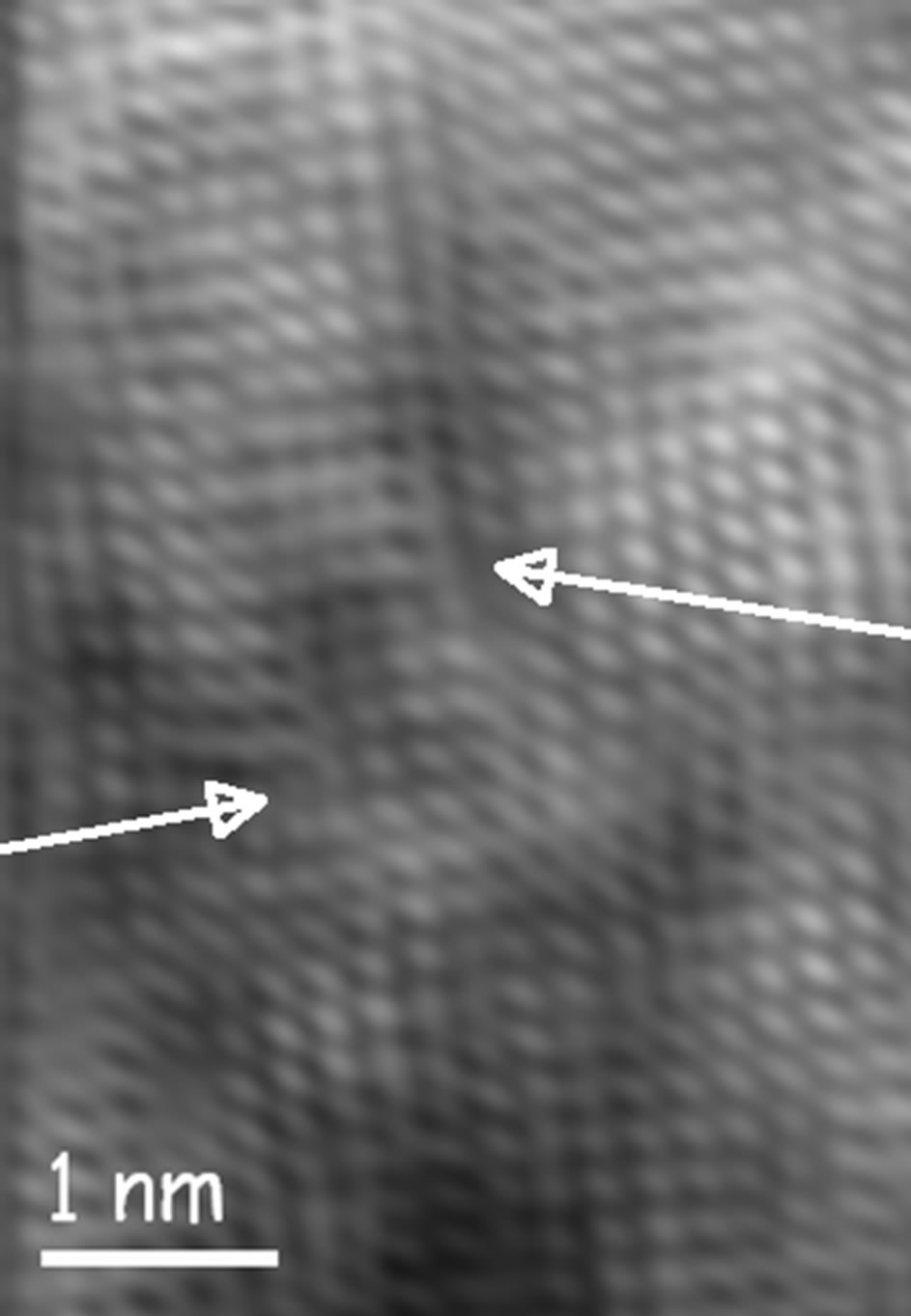
Figure 16. HRTEM cross sectional view (filtered) of TiC/ VC@Sapphire after annealing. Inserted half planes of edge dislocations were indicated by arrows. Light spots represent atom positions.
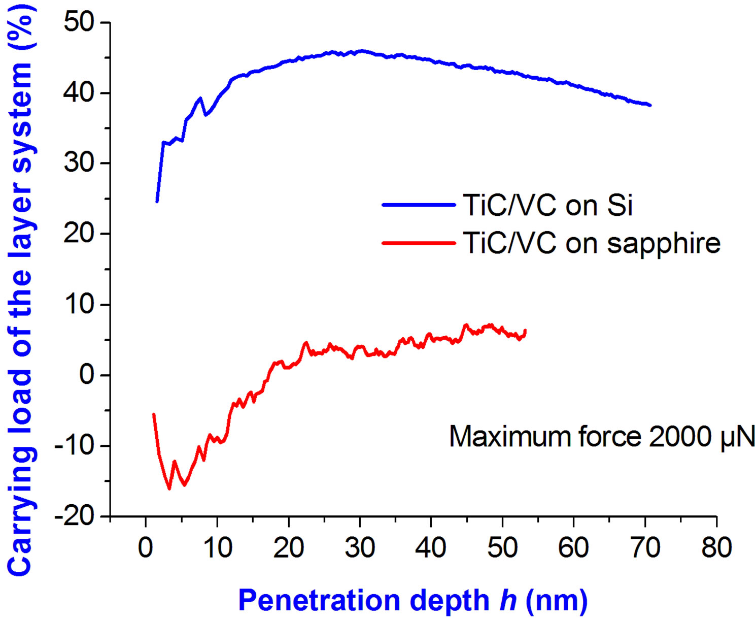
Figure 17. Relative load difference at a given penetration depth h between TiC/VC-covered substrates Si and sapphire and uncovered substrates vs h. Negative values of carrying load are artifacts due to uncertainties of measurement for h < 20 nm. Results refer to a maximum normal force of 2 mN. During the present study, we have investigated F(h) curves up to F = 16 mN.
the following results seem of relevance to the present material. At the beginning of the indentation process, amorphization took place very close to the indenter/layer interface. This is, however, hard to detect experimentally. Comparison of Ti-Ti and Ti-C pair correlation functions under stress and after stress relief indicated some persistence of disorder after deformation. Peak values of those functions behave like interatomic distances prior to and after annealing (cf. Figure 7).
Glide bands and dislocations showed up as expected from slip in real TiC single crystals [32], obeying the constraint of preserving stoichiometry. Note that the single layer thickness dealt with was 4 nm [31], i.e., λ = 8 nm is a little below the period, where Hall-Petch applies according to the present results. Authors presume that, in addition to dislocation movement, some other not specified mechanisms should be active. A grain-like substructure of MuLs weakens the system compared to a defectfree single crystal. This might explain why hardness increased after annealing. On the other hand, looking at Figure 13, smaller subgrains may give rise to higher dislocation density in the λ > 10 nm region and hence to higher H values. Columnar walls in the layer structure, as to be seen in Figure 13, act as obstacles to plastic deformation.
4. Conclusion
By coating silicon and sapphire single crystals with TiC/ VC MuLs, nanohardness was found enhanced for indentation depths up to the total layer thickness, whereas Young’s modulus as derived from force-penetration curves remained almost constant. The contact pressure to start plastic deformation was increased by covering the substrate. A weak superlattice hardening effect of the MuLs has been observed for sapphire. The MuL period of maximum hardness amounted to about 10 nm or less. Hardness enhancement for periods above this value could be attributed to a Hall-Petch behavior, at least for annealed MuLs on sapphire. Reduction of hardness for small MuL periods goes along with the loss of interphase boundaries. The microstructure of MuLs is characterized by a layer substructure consisting of crystalline and some amorphous parts. Interatomic distances in TiC and VC layers approach each other for small MuL periods like in solid solutions. Taking recent computer simulations of a similar system and present TEM images together, our view is supported that dislocations play a distinct role in this material.
5. Acknowledgements
The authors would like to thank the German Research Foundation (DFG) for financial support. A.B. gratefully acknowledges the hospitality of the Fraunhofer-Institutfür Werkstoff und Strahltechnik IWS Dresden and the competent support to prepare the samples. He also enjoyed assistance of the staff of HASYLAB, when doing EXAFS studies. We are also thankful to Dr. B. Wolf for various help with the nanoindentation technique, to Dr. A. Levin for his support of reflectometry studies, to Dr. K. Helming for texture analysis. Ms. Heide Müller is thanked for her skillful preparation of HRTEM samples. The stimulating collaboration with Prof. S. Schmauder and Dr. P. Kizler is also thankfully mentioned.
REFERENCES
- A. F. Jankowski and T. Tsakalakos, “The Effect of Strain on the Elastic Constants of Noble Metals,” Journal of Physics F: Metal Physics, Vol. 15, No. 6, 1985, pp. 1279- 1292. doi:10.1088/0305-4608/15/6/013
- W. D. Sproul, “Reactive Sputter Deposition of Polycrystalline Nitride and Oxide Superlattice Coatings,” Surface and Coatings Technology, Vol. 86-87, 1996, pp. 170-176. doi:10.1016/S0257-8972(96)02977-5
- S. A. Barnett, “Physics of Thin Films,” M. H. Francombe and J. L. Vossen, Eds., Vol. 17, Academic Press, San Diego, 1993.
- L. Hultman, C. Engström and M. Odén, “Mechanical and Thermal Stability of TiN/NbN Superlattice Thin Films,” Surface and Coatings Technology, Vol. 133-134, 2000, pp. 227-233. doi:10.1016/S0257-8972(00)00935-X
- U. Helmersson, S. Todorova, S. A. Barnett, J.-E. Sundgren, L. C. Markert and J. E. Greene, “Growth of Single-Crystal TiN/VN Strained Layer Superlattices with Extremely High Mechanical Hardness,” Journal of Applied Physics, Vol. 62, No. 2, 1987, pp. 481-484. doi:10.1063/1.339770
- J. S. Koehler, “Attempt to Design a Strong Solid,” Physical Review B, Vol. 2, No. 2, 1970, pp. 547-551.
- A. Misra, J. P. Hirth and R. G. Hoagland, “LengthScale-Dependent Deformation Mechanisms in Incoherent Metallic Multi-Layered Composites,” Acta Materialia, Vol. 53, No. 18, 2005, pp. 4817-4824. doi:10.1016/j.actamat.2005.06.025
- H. Ljungcrantz, C. Engström, L. Hultman, M. Olsson, X. Chu, M. S. Wong and W. D. Sproul, “Nanoindentation Hardness, Abrasive Wear, and Microstructure of TiN/NbN Polycrystalline Nanostructured Multilayer Films by Reactive Magnetron Sputtering,” Journal of Vacuum Science and Technology A, Vol. 16, No. 5, 1998, pp. 3104- 3113.
- G. Abadias, A. Michel, C. Tromas, C. Jaouen and S. N. Dub, “Stress, Interfacial Effects and Mechanical Properties of Nanoscale Multilayered Coatings,” Surface and Coatings Technology, Vol. 202, No. 4-7, 2007, pp. 844- 853. doi:10.1016/j.surfcoat.2007.05.068
- K. N. Strafford, “Tribological Properties of Coatings— Expectations, Performance and the Design Dilemma,” Surface and Coatings Technology, Vol. 81, No. 1, 1996, pp. 106-117. doi:10.1016/0257-8972(95)02651-7
- A. R. Phani, J. E. Krzanowski and J. J. Nainaparampil, “Structural and Mechanical Properties of TiC and Ti-Si-C Films Deposited by Pulsed Laser Deposition,” Journal of Vacuum Science and Technology A, Vol. 19, No. 5, 2001, pp. 2252-2258. doi:10.1116/1.1382876
- S. Garcia-Manyes, A. G. Güell, P. Gorostiza and F. Sanz, “Nanomechanics of Silicon Surfaces with Atomic Force Microscopy: An Insight to the First Sates of Plastic Deformation,” Journal of Chemical Physics, Vol. 123, No. 11, 2005, pp. 114711-114717. doi:10.1063/1.2035094
- S. Dub, V. Brazhkin, N. Novikov, G. Tolmachova, P. Litvin, L. Lityagina and T. Dyuzheva, “Comparative Studies of Mechanical Properties of Stishovite and Sapphire Single Crystals by Nanoindentation,” Journal of Superhard Materials, Vol. 32, No. 6, 2010, pp. 406-414. doi:10.3103/S1063457610060067
- P. Paufler and A. Belger, “Superhard Materials,” Proceedings of the 7th Vietnamese-German Seminar on Physics and Engineering, 28 March-3 April 2004, Halong Vietnam, pp. 25-28.
- J. Tang, J. S. Zabinski and J. E. Bultman, “TiC Coatings Prepared by Pulsed Laser Deposition and Magnetron Sputtering,” Surface and Coatings Technology, Vol. 91, No. 1, 1997, pp. 69-73. doi:10.1016/S0257-8972(96)03124-6
- D. C. Meyer and P. Paufler, “X-Ray Characterization of Nanolayers,” H. S. Nalwa, Ed., Encyclopedia of Nanoscience and Nanotechnology, Vol. 10, No. 1, 2004, pp. 655- 680.
- A. A. Levin, P. Paufler and D. C. Meyer, “Low-Temperature Domain Behaviour of a SrTiO3 (001) Single Crystal Plate,” Physica B, Vol. 393, No. 1-2, 2007, pp. 373-381. doi:10.1016/j.physb.2007.01.029
- K. Helming, “Personal Communication”.
- K. Helming and U. Preckwinkel, “Texture Analysis with Area Detectors,” Solid State Phenomena, Vol. 105, 2005, pp. 71-76. doi:10.4028/www.scientific.net/SSP.105.71
- A. Belger, T. Sebald, P. Paufler, H. Mai and E. Beyer, “Polarized EXAFS Studies of TiC/VC-Multilayers,” HASYLAB Annual Report, Part 1, 2001, pp. 783-784.
- N. K. Mukhopadhyay and P. Paufler, “Microand Nanoindentation Techniques for Mechanical Characterisation of Materials,” International Materials Reviews, Vol. 51, No. 4, 2006, pp. 209-245. doi:10.1179/174328006X102475
- I. P. Shakhverdova, P. Paufler, R. S. Bubnova, S. K. Filatov, A. A. Levin and D. C. Meyer, ”Mechanical Properties of Single Crystalline and Glassy Lithium Triborate,” Crystal Research and Technology, Vol. 43, No. 4, 2008, pp. 339-349. doi:10.1002/crat.200711104
- W. C. Oliver and G. M. Pharr, “An Improved Technique for Determining Hardness and Elastic Modulus Using Load and Displacement Sensing Indentation Experiments,” Journal of Materials Research, Vol. 7, No. 6, 1992, pp. 1564-1583. doi:10.1557/JMR.1992.1564
- E. Meyer, “Untersuchungen über Härteprüfung und Härte,” Zeitschrift des Vereins Deutscher Ingenieure, Vol. 52, No. 17, 1908, pp. 645-654, 740-748, 835-844.
- “Elastica,” Software Package, Version 2.1. Asmec Germany, 2003. www.asmec.de
- A. M. Korsunsky, M. R. McGurk, S. J. Bull and T. F. Page, “On the Hardness of Coated Systems,” Surface and Coatings Technology, Vol. 99, No. 1, 1998, pp. 171-183. doi:10.1016/S0257-8972(97)00522-7
- E. O. Hall, “The Deformation and Ageing of Mild Steel. III Discussion of Results,” Proceedings of the Physical Society London, Vol. 64, No. 381, 1951, pp. 747-753.
- N. J. Petch, “The Cleavage Strength of Polycrystals,” Journal of the Iron and Steel Institute, Vol. 174, 1953, pp. 25-28.
- T. H. Courtney, “Mechanical Behavior of Materials,” McGraw Hill Publ. Co., Singapore, 1990.
- J. C. M. Li, “Petch Relation and Grain Boundary Sources,” Transactions of the Metallurgical Society of AIME, Vol. 227, 1963, pp. 239-247.
- P. Kizler and S. Schmauder, “Simulation of the Nanoindentation of Hard Metal Carbide Layer Systems—The Case of Nanostructured Ultra-Hard Carbide Layer Systems,” Computational Materials Science, Vol. 39, 2007, pp. 205-213. doi:10.1016/j.commatsci.2006.03.027
- D. K. Chatterjee, M. G. Mendiratta and H. A. Lipsitt, “Deformation Behaviour of Single Crystals of Titanium Carbide,” Journal of Materials Science, Vol. 14, No. 9, 1979, pp. 2151-2156. doi:10.1007/BF00688420
NOTES
*Corresponding author.