Circuits and Systems
Vol.09 No.08(2018), Article ID:86609,7 pages
10.4236/cs.2018.98012
New Current Mode Lossy Integrator Employing CDDITA
Kuldeep Panwar1, Dinesh Prasad1*, Mayank Srivastava2, Zainab Haseeb1
1Department of Electronics and Communication Engineering, Faculty of Engineering and Technology, Jamia Millia Islamia, New Delhi, India
2Department of Electronics and Communication Engineering, NIT, Jamshedpur, India

Copyright © 2018 by authors and Scientific Research Publishing Inc.
This work is licensed under the Creative Commons Attribution International License (CC BY 4.0).
http://creativecommons.org/licenses/by/4.0/


Received: July 8, 2018; Accepted: August 10, 2018; Published: August 13, 2018
ABSTRACT
This work presents a novel current-mode (CM) lossless integrator that uses one current differencing differential input transconductance amplifier (CDDITA) and one grounded capacitor. The configuration based on single active element has several advantages from the aspect of monolithic integration, few are: reduced power consumption, chip miniaturization. Employment of grounded capacitor is also beneficial for monolithic integration. Specifying some of the key features of integrator proposed are: 1) purely resistorless, 2) electronically tunable, 3) current output available at the port having high impedance, and 4) excellent performance under non-ideal conditions. So, a resister-less current mode lossy integrator with electronic control employing single CDDITA has been proposed in this paper. The verification of workability of the proposed current mode integrator is well explained by the help of SPICE simulations using TSMC CMOS 0.18 µm technology node.
Keywords:
Current Differencing Differential Input Transconductance Amplifier, Lossy Integrator, Electronic Tunability, Grounded Capacitor

1. Introduction
Active RC Integrator is an extremely versatile circuit element that is employed in development and synthesis of numerous analog signal processing as well as generation circuits that include active filters, quadrature oscillators, waveform generators and many more. Various voltage or current mode integrator circuits based on traditional and modern active components has been proposed in literature. An OP-AMP based integrator was proposed in [1] . Some current conveyor (CCII) based integrator were proposed in [2] [3] [4] [5] [6] . Differential voltage current conveyor (DVCC) was also proposed in literature [7] . Some integrator circuits employing modern active elements like current differential buffered amplifier (CDBA) [8] , multiplication mode current conveyor (MMCC) [9] , current controlled current differential buffered amplifier (CCCDBA) [10] , differential difference current conveyor (DDCC) [11] , current differential transconductance amplifier (CDTA) [12] , current follower transconductance amplifier (CFTA) [13] , CCCCTA [14] and current feedback operational amplifier (CFOA) [15] have been proposed in the literature available till date.
But the circuit configurations available with us possess few disadvantages like: 1) they uses greater than 1 active element, 2) greater than 1 passive element, 3) floating capacitors are used which increases chip area, 4) no electronic tenability, 5) matching constraint required, 6) poor non ideal performance, 7) exclusive current output at very high impedance terminal is unavailability (in case of CM integrator).
Hence, the goal of this manuscript is to remove disadvantages mentioned above, hence it possess following advantages:
1) Only one CDDITA is used;
2) Just one capacitor is used;
3) Realization is purely free of resistor;
4) Grounded capacitor used, reduces chip area;
5) Gain is electronically tunable;
6) Better performance in non ideal case;
7) Current output signal at high impedance port is available.
CDDITA is new generation ABB and its idea was proposed in [16] . It is an extension of CDTA which has been a popular ABB in last decade. The electrical symbol of CDDITA is shown in Figure 1. It has two virtually grounded low input impedance terminals P and N, two high impedance intermediate terminals Z and V and two high impedance output terminals X+ and X−.
The behavioral model of CDDITA is shown in Figure 2, which illustrates that input stage is a current differencing unit and the output stage is an OTA.
The voltage current relationships between different ports of CDDITA can be given by following equation set:
(1)
(2)
(3)
(4)
The CMOS realization of CDDITA has been shown in Figure 3.
The applications of CDDITA in analog signal processing/signal generation have been proposed in [17] [18] .
2. Proposed Current-Mode Integrator
The circuit of lossy integrator proposed is shown in Figure 4.

Figure 1. Block diagram of CDDITA.
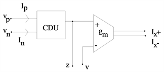
Figure 2. Behavioral model of CDDITA.

Figure 3. CMOS implementation of CDDITA.

Figure 4. Proposed CM lossy Integrator.
Through proper analysis of circuit following expression is yielded the for output current;
(5)
From Equation (5), it becomes clear that the gain of proposed integrator can be tuned electronically by gm1, which is adjusted by bias currents of CDDITA. Output current “Iout” is explicitly available at high impedance “X−” port is shown in Figure 3. Hence, there is no additional need of follower is to use this output.
3. Non-Ideal Analysis and Sensitivity Calculations
Under non-ideal condition the CDDITA is defined by following equations of VDTA modified as
(6)
(7)
(8)
where “ ” and “ ” are the trans-conductance error gains and “αp” and “αn” are errors in current transfer. These values are just slightly less than that of unity.
The current output transfer function of the presented paper under the influence of ideal conditions is given as
(9)
It is clear from Equation (9) that even; the proposed configuration has an ability to simulate an ideal CM integrator under the non-ideal conditions, with adjustable tunable gain. So, the nature of presented circuit remains unaffected in the non-ideal conditions.
4. Simulation Results
The presented circuit is verifying by simulating it by employing CMOS CDDITA (shown in Figure 3) with ±3 V DC supply voltage. All the biasing currents of CDDITA are chosen as 100 µA and the value of capacitor “C” is selected as 0.1 nF. To study the input output relation a rectangular input current signal (shown in Figure 5) of ±0.5 mA is used. The output current (Iout) is shown in Figure 6.

Figure 5. Input rectangular current pulse of amplitude ±0.5 mA and duration 4 µs (Iinput).

Figure 6. Output triangular current pulse (Ioutput).
5. Conclusion
A CDDITA based current mode lossy integrator circuit that uses single CDDITA and grounded capacitor has been presented in this manuscript. The proposed circuit has following features: no requirement of any resistor, electronically controllable gain and explicit current mode (CM) output at a high impedance port that is suitable for cascading and no requirement of component matching constraint. The designed circuit configuration shows good non-ideal behavior and even in that conditions the circuit can simulate a lossless CM integrator. The analysis has been successfully verified by PSPICE simulation using TSMC CMOS of 0.18 μm process parameters. For simulation purpose CMOS CDDITA has been used with biasing current of 100 µA and supply voltage of ±3 V DC.
Acknowledgements
This research is supported by the “Young Faculty Research Fellowship and Research/Contingency Grant” to Jamia Millia Islamia, under “Visvesvaraya PhD Scheme for Electronics and IT” in 2015-16.
Conflicts of Interest
The authors declare no conflicts of interest regarding the publication of this paper.
Cite this paper
Panwar, K., Prasad, D., Srivastava, M. and Haseeb, Z. (2018) New Current Mode Lossy Integrator Employing CDDITA. Circuits and Systems, 9, 117-123. https://doi.org/10.4236/cs.2018.98012
References
- 1. Sanyal, S.K., Sarker, U.C. and Nandi, R. (1990) Increased Time-Constant Dual-Input Integrators. IEEE Transactions on Instrumentation and Measurement, 39, 672-673. https://doi.org/10.1109/19.57257
- 2. Abuelmaatti, M.T. (1994) On the Realization of Current-Mode Integrator Using Current Conveyors. Active and Passive Electronic Component, 17, 79-82. https://doi.org/10.1155/1994/64935
- 3. Makris, C.A. and Toumazou, C. (1990) High Frequency, Precision Integrators Using Current Conveyor Compensation Techniques. IEEE International Symposium on Circuits and Systems. https://doi.org/10.1109/ISCAS.1990.112016
- 4. Lee, J.Y. and Tsao, H.W. (1992) True RC Integrators Based on Current Conveyors with Tunable Time Constants Using Active Control and Modified Loop Technique. IEEE Transactions on Instrumentation and Measurement, 41, 709-714. https://doi.org/10.1109/19.177348
- 5. Liu, S.L. and Hwang, Y.S. (1994) Dual-Input Differentiators and Integrators with Tunable Time Constants Using Current Conveyors. IEEE Transactions on Instrumentation and Measurement, 43, 650-654. https://doi.org/10.1109/19.310164
- 6. Sedra, A. and Smith. K.C. (1970) A Second-Generation Current Conveyor and Its Applications. IEEE Transactions on Circuit Theory, 132-134. https://doi.org/10.1109/TCT.1970.1083067
- 7. Minaei, S. (2004) Dual-Input Current-Mode Integrator and Differentiator Using Single DVCC and Grounded Passive Elements. IEEE MELECON, Dubrovnik, 123-126.
- 8. Nandi, R., Das, S., Kar, M. and Das, S. (2010) Active-R Tunable Integrators Using a Current Differencing Buffered Amplifier. International Journal of Electronics, 97, 129-137. https://doi.org/10.1080/00207210903168835
- 9. Venkateswaran, P., Nandi, R. and Das, S. (2012) New Integrators and Differentiators Using a MMCC. Circuits and Systems, 3, 288-294. https://doi.org/10.4236/cs.2012.33040
- 10. Ramola, V. and Mishra, S. (2012) Design of CCCDBA Based Voltage Mode Differentiator and Integrator. Proceedings of the International Conference on Advances in Electronics, Electrical and Computer Science Engineering—EEC, 109-112.
- 11. Yuce, E. (2014) Novel Instrumentation Amplifier and Integrator Circuits Using Single DDCC and Only Grounded Passive Elements. Indian Journal of Pure and Applied Physics, 52, 767-775.
- 12. Biolek, D., Keskin, A.U. and Biolkova, V. (2012) Quadrature Oscillator Using CDTA-Based Integrators. WSEAS Transaction on Electronics, 3, 463-469.
- 13. Uttaphut, P. (2012) Realization of Electronically Tunable Current-Mode Multiphase Sinusoidal Oscillators Using CFTAs. World Academy of Science, Engineering and Technology, 6, 643-646.
- 14. Uttaphut, P. (2012) New Current Mode Multiphase Sinusoidal Oscillators Based on CCCCTA-Based Lossy Integrators. Przeglad Elektrotechniczny (Electrical Review), 291-295.
- 15. Lee, J.L. and Liu, S.H. (2001) Integrator and Differentiator with Time Constant Multiplication Using Current Feedback Amplifier. Electronics Letters, 37, 331-332. https://doi.org/10.1049/el:20010252
- 16. Biolek, D., Senani, R., Biolkova, V. and Kolka, Z. (2008) Active Elements for Analog Signal Processing; Classification, Review and New Proposals. Radioengineering, 17, 15-32.
- 17. Panwar, K., Prasad, D., Bhaskar, D.R. and Srivastava, M. (2017) Novel Single Resistance Controlled Oscillator Employing MCDDITA. Journal of Engineering Technology, 6, 352-358.
- 18. Prasad, D., Panwar, K., Bhaskar, D.R. and Srivastava, M. (2015) CDDITA-Based Voltage Mode First Order All-Pass Configuration. Circuits and Systems (USA), 6, 252-256. https://doi.org/10.4236/cs.2015.611025
Nomenclature
VP: Voltage at “P” terminal
VN: Voltage at “N” terminal
VZ: Voltage at “Z” terminal
VV: Voltage at “V” terminal
IP: Current at “P” terminal
IN: Current at “N” terminal
IZ: Current at “Z” terminal
Iin: Input current
Iout: Output current
gm: Transconductance of CDDITA
α, β: Current gain errors