Circuits and Systems
Vol.5 No.4(2014), Article ID:44304,7 pages DOI:10.4236/cs.2014.54009
Experimental Demonstration of  Based Noise Analysis
Jack Ou1, Pietro M. Ferreira2, Jui-Chu Lee3
1Department of Engineering Science, Sonoma State University, Rohert Park, USA
2IEMN, UMR CNRS 8520 Department of DHS, University of Lille, Lille, France
3IBM Microelectronics Essex Junction, New York, USA
Email: jack.ou@sonoma.edu, maris@ieee.org, juichu@us.ibm.com
Copyright © 2014 by authors and Scientific Research Publishing Inc.
This work is licensed under the Creative Commons Attribution International License (CC BY).
http://creativecommons.org/licenses/by/4.0/


Received 20 January 2014; revised 20 February 2014; accepted 28 February 2014
ABSTRACT
Recent studies using BSIM3 models have suggested that noise depends on the transconductanceto-drain ratio  of a transistor. However, to the best of our knowledge, no experimental result demonstrating
  dependent noise previously observed in simulation is available in the literature. This paper examines the underlying principles that make it possible to analyze noise using
  based noise analysis. Qualitative discussion of normalized noise is presented along with experimental results from a 130 nm CMOS process. A close examination of the experimental results reveals that the device noise is width independent from 1 Hz to 10 kHz. Moreover, noise increases as
  is reduced. The experiment observation that noise is width independent makes it possible for circuit designers to generate normalized parameters that are used to study noise intuitively and accurately.
Keywords: Design Methodology; Noise Analysis; Flicker Noise

1. Introduction
In integrated circuits, noise phenomena are caused by small current and voltage fluctuations that are generated within the devices themselves. At low frequencies, the noise spectrum is dominated by the flicker noise. At high frequencies, the noise spectrum is dominated by the thermal noise. The study of noise is important because it ultimately determines the smallest signal that a circuit can amplified without significant deterioration in signal quality [1] .
From a designer’s perspective, noise is a property of the circuit that must be designed carefully along with other circuit parameters such as gain, power dissipation, speed, and linearity. Noise analysis is particularly challenging in sub-micron CMOS circuit design because it involves parameters that depend on the bias condition of a transistor as well as the geometry of a transistor. In the absence of an easy-to-use model for accurate backof-the-envelope noise calculation, designers often explore design space using arduous circuit simulations. Overreliance on circuit simulator can be problematic, potentially luring inexperienced designers to dive into simulation without understanding basic trade-offs in properly optimized circuits.
1.1. A Brief Overview of Related Work
In 1996, Silveira et al. proposed a powerful transconductance-to-drain current  technique that has since become the basis of many later developments in structured analog circuit design [2] . The so-called “
 design approach” was originally developed to help designers to size up transistors quickly with good accuracy and to calculate parameters such as small signal gain and bandwidth. Recently, it has found applications in large signal behavior of a power amplifier [3] , phase noise optimization of an LC oscillator [4] , MOSFET nonlinearity characterization [5] , MOSFET variability and ageing degradations [6] . A simple
  CAD tool has also been developed recently to optimize analog circuits without lengthy simulations [7] . A book dedicated to
  methodology has also been published [8] .
A  based noise analysis was reported in 2011 [9] . Bias dependent thermal noise coefficient
  and device noise corner frequency
  were used to characterize MOSFET noise. In 2012, Alvarez and Abusleme published a formulation of
  based noise analysis using normalized noise power instead of
  and
and  [10] . In [10] , noise curves for a set of transistors are pre-computed by means of SPICE simulations, scaled for the appropriate device parameters using the
  technique, and finally, noise is computed using interpolations within the curves. The work in [10] was applied in the context of charge amplifiers in [11] .
1.2. Main Contributions of This Paper
To the best of our knowledge, what is currently known in the literature with respect to  based noise analysis is derived from either HSPICE analysis [10] or BSIM simulation ([9] and [11] ). According to a study conducted by Rhayem et al. [12] , each noise model has a different accuracy with respect to measured data. For example, the SPICE noise model is not accurate for all regions of operation for both NMOS and PMOS. The HSPICE noise model cannot predict noise accurately for PMOS. For NMOS, the model can be used if a subcircuit includes access resistances and their excess noise sources. Even though the BSIM3v3 noise model is more accurate than either the SPICE noise model or HSPICE noise model, the most accurate portrayal of a device’s noise is through measurement.
This paper presents an experimental study of  based noise. In particular, we present wafer measurement data from a 130 nm CMOS process utilizing both NMOS and PMOS transistors. Two experimental results are presented. First, we present the experimental data to show that the normalized noise is independent of a transistor’s gate width. Second, we present the experimental data to show that the normalized noise increases as a transistor’s
  is reduced.
The organization of this paper is as follows: Section 2 provides a review of  analysis, followed by a discussion of thermal noise and flicker noise in the context of
  based noise analysis. Section 3 shows the experimental results on
  noise. Finally, we present our conclusions.
2. Formulation of Noise Measurement
We begin this section with a review of fundamentals of  analysis. We point out in this section that noise current
  of an MOS transistor is width dependent, it is therefore not a valid
  parameter. In order to make the noise current a valid
  parameter, we normalize the noise by dividing
  by
by . The details are shown below.
2.1. Fundamentals of  Analysis
The  principle is applicable to parameters which are independent of the width
  of a transistor. Figure 1 shows a transistor with a transconductance
 , a drain-to-source conductance
 , and a current
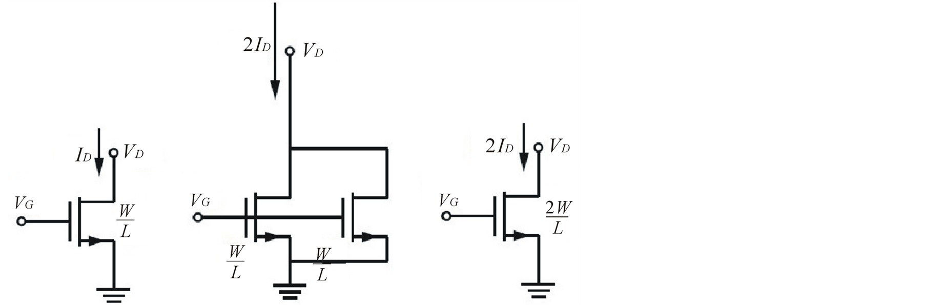
Figure 1. Transistors biased at the same .
.
 biased at a gate-to-source voltage
  and a drain-to-source
 . If an identical device is connected in parallel so both devices are biased at the same
  and
and , both devices have the same
 ,
,  and the same
 . Since the devices are connected in parallel, they can be treated as one device with an aspect ratio of
 . The effective transconductance over current ratio is
  for both the merged device and the stand alone device because
  and
and  are doubled. The drain-to-source conductance is also doubled for the merged device. Therefore the intrinsic gain
  is identical for both the stand alone device and the merged device. As long as transistors are biased at the same
 , they will have the same
 . This observation is true for any two parameters whose ratio depend solely on the
  and not on the width of a transistor. Once a transistor of a given
  is characterized over a range of
 , the
, the  based parameters can be generalized to a transistor of an arbitrary
 , assuming that
  remains constant. The
  methodology will hold as long as the parameter of interest scales with
 .
.
2.2. Thermal Noise
The MOSFET noise arises from thermal noise fluctuations in the channel. It can be shown that the thermal noise at the drain terminal is [13] ,
 (1)
(1)
where  is the Boltzmann constant,
  is the temperature,
  is the transconductance, and
  is the biasdependent noise parameter. According to this model, the
  approaches 1 when the drain-to-source voltage
  approaches zero and decreases to
  when the device enters the saturation regime. The saturation value of
  is valid for long-channel MOS devices built on lightly doped substrates. Early studies have reported
  values between
  and 4 [14] , but recent studies have shown that by accounting for parasitic resistances,
  is approximately
  for channel lengths equal or greater than 100 nm [15] .
The thermal noise  at the drain terminal of a MOS transistor is
 (2)
(2)
where  is the total inversion layer charge underneath the gate oxide,
  is the length of the transistor, and
  is the mobility. Equation (2) is valid for all regions of operation [13] . The total inversion layer charge
  is obtained by integrating the inversion charge per unit length
  over the length of the channel,
 (3)
(3)
where  is a function of
  and
and , as well as
 , and consequently a function of transistor’s
 . Since
  is proportional to
  (see Equation (3)),
  is proportional to
  according Equation (2). Since
  is proportional to
 ,
,  becomes independent of
 . Equation (2) also shows that
  is inversely proportional to L2. Even though the transconductance of a transistor also depends on the L, it is not inversely proportional to L2. Therefore,
  is a function of L. Once
  of a transistor for a given
  is characterized over a range of
 ;
;  of the transistor can be generalized to a transistor of arbitrary
  as long as L and the
  are constant. We will verify this observation in Section 3. This width-independent property is the crucial link to the
  design methodology described earlier.
2.3. Flicker Noise
Since MOSFETs are surface-conduction devices, flicker noise is important at low frequencies. The flicker noise present at a MOSFET can be expressed into a noise current at the drain terminal of a transistor with
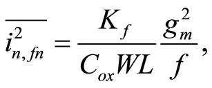 (4)
(4)
where  is a process dependent constant and
  is the oxide capacitance. Equation (4) can be rewritten to explicitly show its dependence on
  parameters as
 (5)
(5)
If we divide  by
by , we find
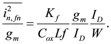 (6)
(6)
Thus, we have in  a parameter which depends exclusively on the
  of a transistor. It should be pointed out that
  (the current density) is also a function of
 . Furthermore, Equation (6) implies that any two transistors, regardless of their widths (
 ), theoretically exhibits the same
  if they are biased at the same
 . This is a useful property to compare measured noise of different transistors biased at the same
 .
.
3. Experimental Results
Section 2 identifies  as a function of
  parameter satisfying all characteristics described in Section 2.1. The
  is used here as a parameter to compare noise characteristics of different transistors. In order to experimentally prove such formulations, ten NMOS transistors from a CMOS 130 nm process are chosen from three different wafers. Each transistor has a length of 0.12 μm and a width of 10 μm. The gate of each transistor is biased at 0.45 V and the drain of each transistor is biased at 1.0 V. The source terminal is grounded
 . We present the noise as a function of
  and as a function of the frequency. Both
  and
and  are determined experimentally without curve fitting.
3.1. Noise as a Function of 
The single-finger and ten-finger NMOS transistors from a 0.13 μm CMOS process are measured, and separated into two sets of data. The noise current at the drain terminal is measured comparing a single-finger  and ten-finger
  data sets biased at the same voltages.
The average ,
,  and
and  of both sets of transistors are shown in Table 1. The dimensions of the transistors are shown in the first row of the table using the format:
 . The total width of each transistor is obtained by multiplying
  by
by . The transistors shown in the fourth column have ten times the width than the transistors in the third column, and hence have ten times the
 ,
,  ,
, . The
. The  and
and  are approximately the same since
 ,
,  and
and  are proportional to the width of a transistor. We conclude that
  dependent parameters (e.g.,
 ) are independent of
 .
.
Having verified that transistors are biased correctly, we investigate  as a function of
 . The
. The  is varied as
  is held constant in order to change
  of a transistor. The drain-current density is measured at 100 Hz as
  is changed. The
  of a 10 μm device is compared to the
  of a 100 μm device. In Figure 2, the average
  (represented with marks) and the standard deviation (represented with error bars) of ten samples are shown.
The  measured at 100 Hz is dominated by flicker noise. Equation (5) suggests that
  is proportional to
  and
and . the current density
  is inversely proportional to
 . Therefore,
  increases as
  is reduced. The 10 μm device exhibits more process variation than the 100 μm device as expected. The close correlation of the 10 μm device and the 100 μm device measurements (see Figure 2) demonstrate that
  are width independent, and therefore
  dependent as stated in Section 2.3.
3.2. Noise as a Function of Frequency
The  of the transistors measured from 1 Hz to 100 kHz are shown in Figure 3. The PMOS devices exhibit less noise than the NMOS devices as previously observed and theoretically expected [13] . Good correlation

Table 1. Comparison of  parameters. NFETs are biased at
  V and
V and  V; PFETs are biased at
  V and
V and  V. Device dimensions:
 .
.
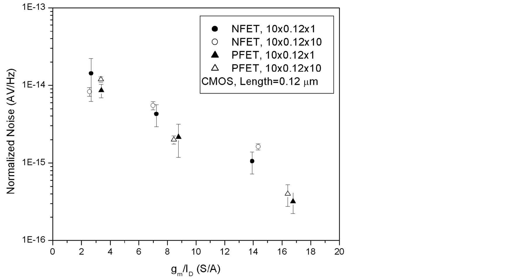
Figure 2. The  comparison over a range of
  for NFET
  V, and PFET
  V.
V.

Figure 3. The  noise compared from 1 Hz to 10 kHz for: NFET
  V, PFET
  V.
V.
between the 10 μm devices and 100 μm devices is presented from 1 Hz to 1 kHz. Our calculation shows that the noise flattening at frequencies higher than 10 kHz is attributed to the noise introduced by the instrumentation amplifier used in the measurement set-up. The close correlation of  from 1 Hz to 1 kHz demonstrates that device noise is width independent.
4. Conclusion
This paper examines the underlying principles that make it possible to study noise using  based noise analysis. Fundamentals of
  analysis were presented, followed by a discussion of normalized thermal noise and normalized flicker noise. Experimental results were shown to demonstrate that noise is indeed width independent from 1 Hz to 10 kHz. Furthermore, noise increases as
  is reduced. The experiment observation that noise is width independent makes it possible for circuit designers to generate normalized parameters that are used to study noise intuitively and accurately.
References
- Gray, P., Hurst, P., Lewis, S. and Meyer, R. (2000) Analysis and Design of Analog Integrated Circuits. John Wiley and Sons, New York.
- Silveira, F., Flandre, D. and Jespers, P.G.A. (1996) A gm/ID Based Methodology for the Design of CMOS Analog Circuits and Its Application to the Synthesis of a Silicon-on-Insulator Micropower OTA. IEEE Journal of Solid-State Circuits, 31, 1314-1319. http://dx.doi.org/10.1109/4.535416
- Barabino, N., Fiorelli, R. and Silveira, F. (2010) Efficiency Based Design Flow for Fully-Integrated Class C RF Power Amplifiers in Nanometric CMOS. Proceedings of IEEE ISCAS, 2010, 2223-2226.
- Fiorelli, R., Peralías, E.J. and Silveira, F. (2011) LC-VCO Design Optimization Methodology Based on the gm/ID Ratio for Nanometer CMOS Technologies. IEEE Transactions on Microwave Theory and Techniques, 59, 1822-1831. http://dx.doi.org/10.1109/TMTT.2011.2132735
- Ou, J. and Farahmand, F. (2012) Transconductance/Drain Current Based Distortion Analysis for Analog CMOS Integrated Circuits. IEEE Proceedings of NEWCAS, June 2012, 61-64.
- Ou, J. and Ferreira, P.M. (2013) Transconductance/Drain Current Based Sensitivity Analysis for Analog CMOS Integrated Circuits. IEEE Proceedings of NEWCAS, June 2013.
- Abdelfattah, O., Shih, I. and Roberts, G. (2013) A Simple Analog CMOS Design Tool Using Transistor Dimension-Independent Parameters. Proceedings of IEEE ISCAS, Beijing, May 2013.
- Jespers, P. (2010) The gm/ID Methodology, a Sizing Tool for Low-Voltage Analog CMOS Circuits. Springer, Louvain-la-Neuve, Belgium.
- Ou, J. (2011) gm/ID Based Noise Analysis for CMOS Analog. IEEE Proceedings of MWSCAS, Seoul, August 2011, 26-29.
- Alvarez, E. and Abusleme, A. (2012) Noise Power Normalisation: Extension of gm/ID Technique for Noise Analysis. Electronics Letters, 48, 430. http://dx.doi.org/10.1049/el.2011.3730
- Alvarez, E., Avila, D., Campillo, H., Dragone, A. and Abusleme, A. (2012) Noise in Charge Amplifiers—A gm/ID Approach. IEEE Transactions on Nuclear Science, 59, 2012. http://dx.doi.org/10.1109/TNS.2012.2208270
- Rhayem, J., Gillon, R., Tack, M., Valenza, M. and Hoffmann, A. (2002) Comments on Existing 1/f Noise Models: SPICE, HSPICE and BSIM3v3 for MOSFETs in Circuit Simulators. European Solid-State Device Research Conference, Firenze, September 2002.
- Tsividis, Y. (1999) Operation and Modeling of the MOS Transistor. McGraw-Hill, New York.
- Dronavalli, S. and Jindal, R.P. (2006) CMOS Device Noise Considerations for Terabit Lightwave Systems. IEEE Transactions on Electron Devices, 53, 623-630. http://dx.doi.org/10.1109/TED.2006.870570
- Tiemeijer, L.F., Havens, R.J., Kort, R.D. and Scholten, A.J. (2005) Improved Y-Factor Method for Wide-Band OnWafer Noise-Parameter Measurements. IEEE Transactions on Microwave Theory and Techniques, 53, 2917-2925. http://dx.doi.org/10.1109/TMTT.2005.854243