Circuits and Systems
Vol.5 No.1(2014), Article ID:41836,6 pages DOI:10.4236/cs.2014.51001
Dual DVCC Based Voltage-Mode Digitally Programmable Biquadratic Filter
Department of Electronics Engineering, Aligarh Muslim University, Aligarh, India
Email: ale.imran23@gmail.com
Copyright © 2014 Ale Imran et al. This is an open access article distributed under the Creative Commons Attribution License, which permits unrestricted use, distribution, and reproduction in any medium, provided the original work is properly cited. In accordance of the Creative Commons Attribution License all Copyrights © 2014 are reserved for SCIRP and the owner of the intellectual property Ale Imran et al. All Copyright © 2014 are guarded by law and by SCIRP as a guardian.
Received November 8, 2013; revised December 8, 2013; accepted December 15, 2013
Keywords: Voltage-Mode; Differential Voltage Current Conveyor (DVCC); Multifunctional Filter; Digitally Controlled Circuits; Current Summing Network
ABSTRACT
The recent advances in IC technology have led to the trend of designing hybrid systems to benefit both analog and the digital domain. Among analog circuits, multifunctional filter along with multiphase oscillator constitutes a building block of critical importance. In this paper, a digitally reconfigurable multi-input-multi-output voltage mode multifunctional biquadratic filter has been presented. The circuit comprises of two differential voltage current conveyors (DVCCs), two grounded capacitors and two floating resistors. The digital controllability is incorporated using a current-summing network (CSN). Tunability of quality factor is achieved by the use of a 3-bit digital control word while keeping the resonant frequency constant. PSPICE simulations using TSMC 0.25 μm CMOS technology have been performed to validate the theoretically predicted results.
1. Introduction
Voltage-mode active filters exhibiting high input impedance are of great interest as a number of cells can be easily cascaded for the realization of the higher order filters. The significance of the digitally controlled blocks can be appreciated in situations where a filter needs to be designed for the given filter parameters, i.e. its cut-off frequency and quality factor. According to the given specifications and the transfer function of the circuit, the values of passive elements are selected to meet the requirements. If any parameter of the circuit is altered, the circuit needs to be designed again and again which is a tedious task. This problem can be alleviated by employing digitally controlled circuits which provide the flexibility to design the circuit for certain discrete values of the parameters instead of the single fixed value in conventional filters. The number of values will depend on the minimum resolution of the control word.
There have been countless applications that involve realization of active transfer functions employing current conveyors, which have received a considerable amount of research attention [1]. The continuous-time analog filter is a ubiquitous circuit component in a vast variety of applications including, but not limited to, noise rejection & signal separation in industrial and measurement circuits, feedback of phase & amplitude control in servo loops, smoothing of digitally generated analog signals, audio signal shaping & sound enhancement, and channel separation & signal enhancement in communication electronics.
Among the several variations of current conveyor, the most successful type is second-generation current conveyor (CCII) introduced by Sedra and Smith [2]. However, when it comes to applications demanding differential or floating inputs like impedance converter circuits and current-mode instrumentation amplifiers, which also require two high input impedance terminals, a single CCII block is no more sufficient. Moreover, these applications employ floating elements to minimize the number of used CCII blocks [3]. Considering the obvious drawbacks of CCIIs, a new building block called differential voltage current conveyor (DVCC) building block was introduced [4]. DVCC is a widely used versatile analog building block whose applications exist in the literature [5-9]. In this paper, the Q-factor of multifunctional filter proposed by Chen et al. [10] is digitally tuned with the help of a Current Summing Network (CSN). The paper is organized as follows. Section 2 presents a brief description about DVCCs. In Section 3, the circuit proposed in [10] by Chen et al. which has been digitally controlled is discussed, followed by Section 4, which gives a brief idea about the operation of the Digitally-Controlled DVCC (DC-DVCC) using CSN. Section 5 deals with the details of the proposed digitally controlled multifunctional biquadratic filter along with its design. Finally, the results are discussed in Section 6, followed by the concluding remarks appearing in Section 7.
2. Differential Voltage Current Conveyor
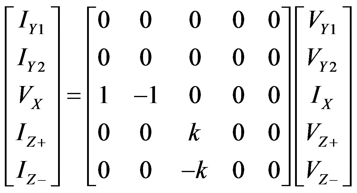
The DVCC is a five-port, widely used analog building block defined by the following matrix equation [4].
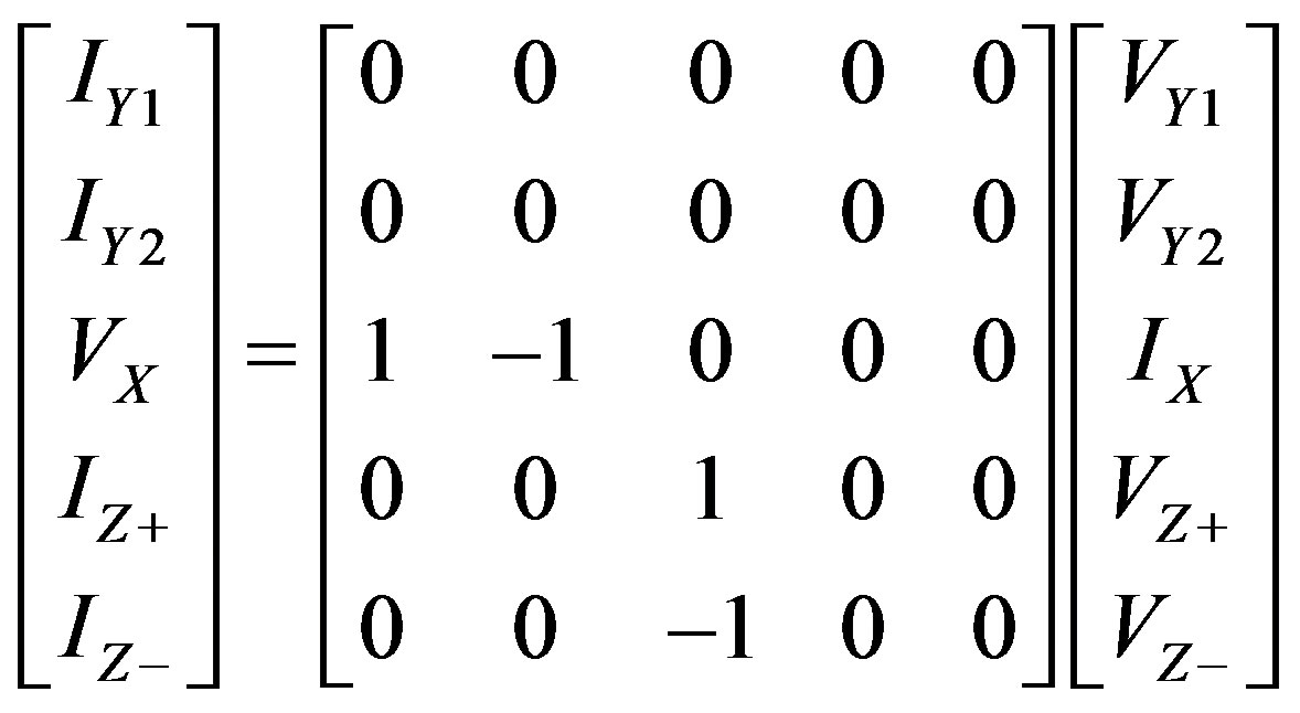 (1)
(1)
The block level implementation of an ideal DVCC is shown in Figure 1, whereas its CMOS transistor realization [4] used in this paper for implementing multifunctional filter is depicted in Figure 2.
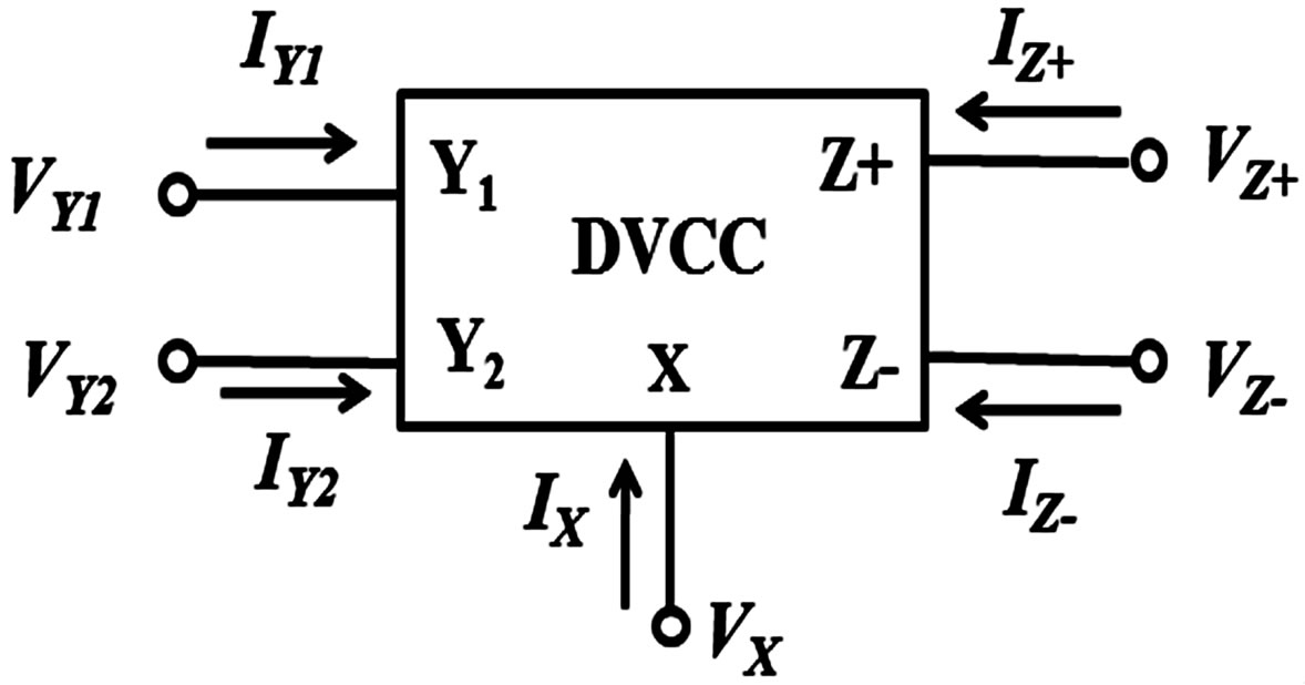
Figure 1. Symbolic representation of the dual output DVCC.
3. CMOS Implementation of DVCC Filter
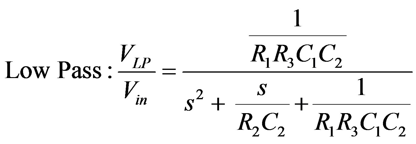
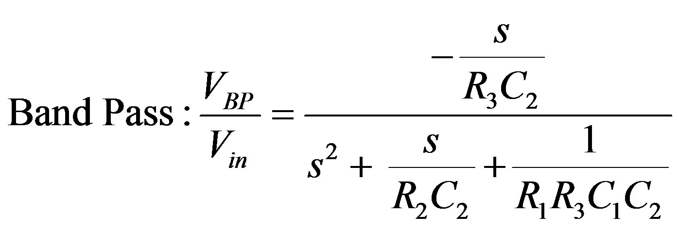
The implemented voltage mode multifunctional filter [10] is shown in Figure 3. Routine analysis of the circuit, yields the following voltage transfer functions of the voltage-mode second order low-pass, high-pass, band-pass and band-reject filters given respectively by Equations (2)-(5).
If Vi1 = Vi3 = Vin(the input voltage signal) and Vi2 = 0, then
 (2)
(2)
 (3)
(3)
 (4)
(4)
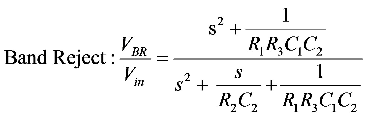 (5)
(5)
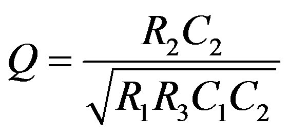
where the quality factor, Q and theresonant angular frequency,  are given by:
 (6)
(6)
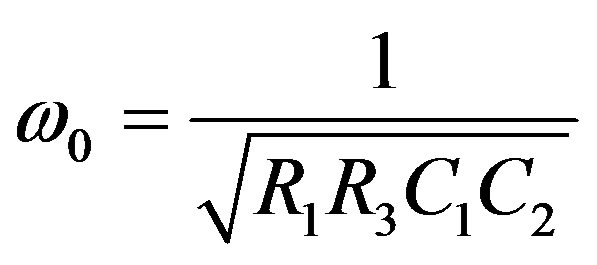 (7)
(7)
It is to be noted that the low-pass, high-pass, band-pass and band reject functions can be simultaneously realized
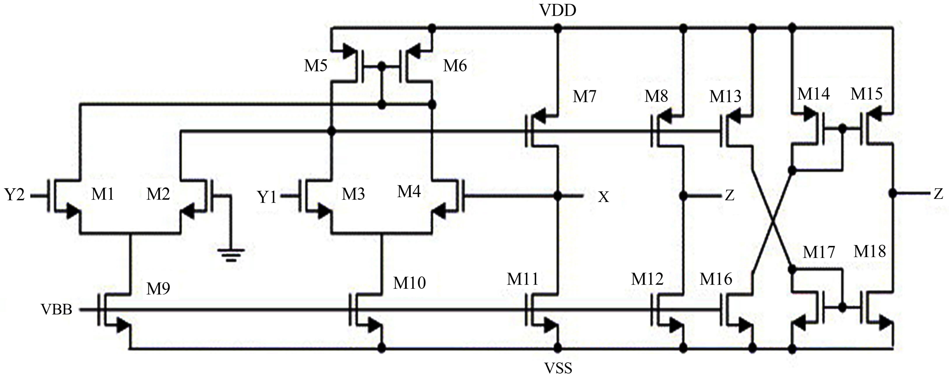
Figure 2. CMOS realization of the dual output DVCC [4].
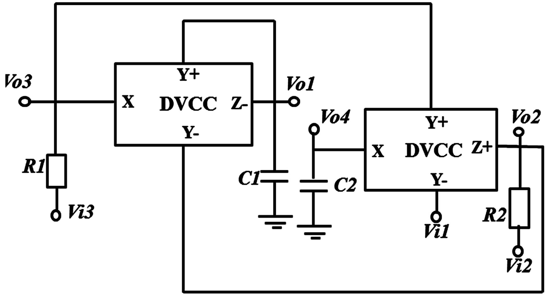
Figure 3. Circuit diagram of voltage mode multifunctional filter with two DVCCs [10].
without changing the circuit configuration. The multifunctional filter has been designed for a cut-off frequency of 1 MHz with C1 = C2 = 15.9 pF, R1 = R2 = 10 kΩ. The responses of the multifunctional filter for the above given design is shown in Figure 4. The circuit has been simulated with the help of 0.25 µm technology. TSMC process parameters using PSPICE package have been used for carrying out the analysis and the results are in conformity with the theoretical analysis.
4. Digitally Programmable DVCC
For introducing the digital control in the multifunctional filter we have used Digitally Controllable DVCC (DCDVCC), shown in Figure 5. It’s basically a 5-terminal analog building block defined by the following relations:
 (8)
(8)
As defined by the characteristics equations in Equation (8), the voltage on the X-terminal realizes the difference of potentials on terminals Y1 and Y2. Furthermore, the current injected at the X-terminal is replicated by a factor of k to the Z-terminals. For the Z+ and Z− terminals, the conveyed current flows in the same and opposite direction respectively, to the current flowing in the X terminal [11].
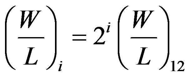
For digitally reconfiguring the DVCC and obtaining a digitally controlled DVCC (DC-DVCC), a Current Summing Network (CSN) has been employed at the Zand Z+ terminal for controlling the current transfer gain parameter k. The gain parameter k can be varied from 1 to (2n – 1), where n represents the number of transistor arrays. The modified circuit of DVCC i.e. Digitally Controlled-DVCC employing a CSN is shown in Figure 6 [11]. The CSN consists of n transistor pairs, the aspect ratios of whose NMOS and PMOS transistors are given by:
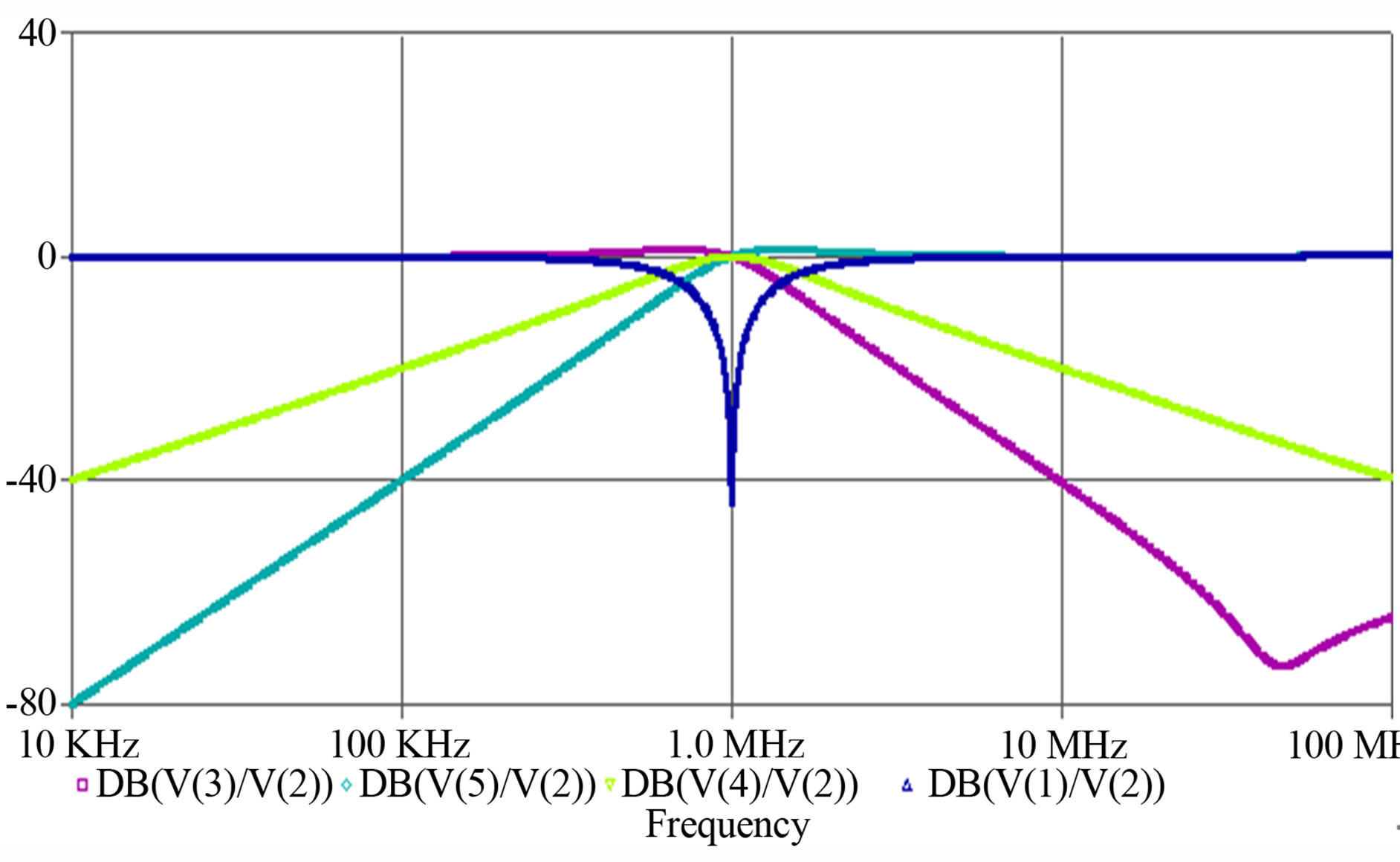
Figure 4. Gain-frequency characteristic (in dB) of the lowpass, high-pass, band-pass and band-reject outputs.
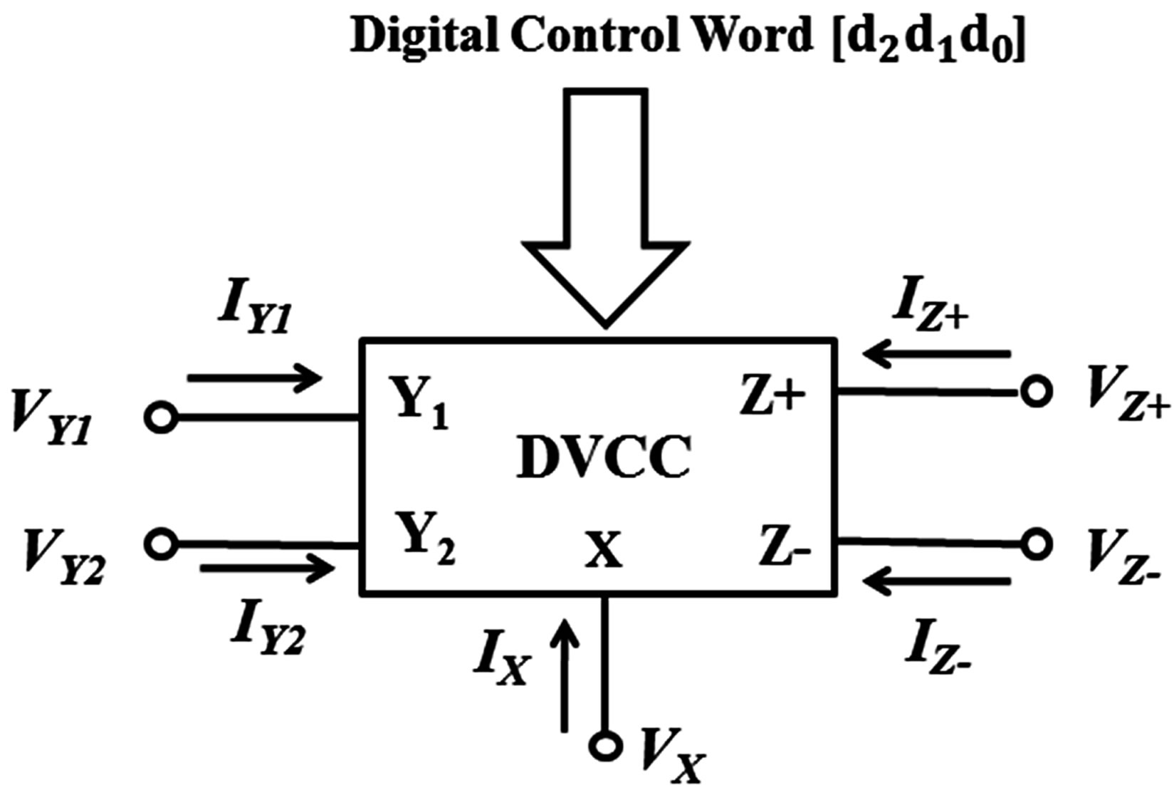
Figure 5. Symbolic representation of the Digitally Programmable DVCC [11].
 (9)
(9)
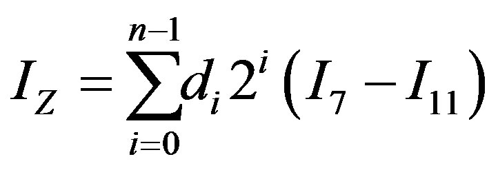
Furthermore, the current at the Z terminal, assumed to be flowing out of the DC-DVCC, can be expressed by:
 (10)
(10)
Therefore, the proposed DC-DVCC provides a current transfer gain, k equal to:
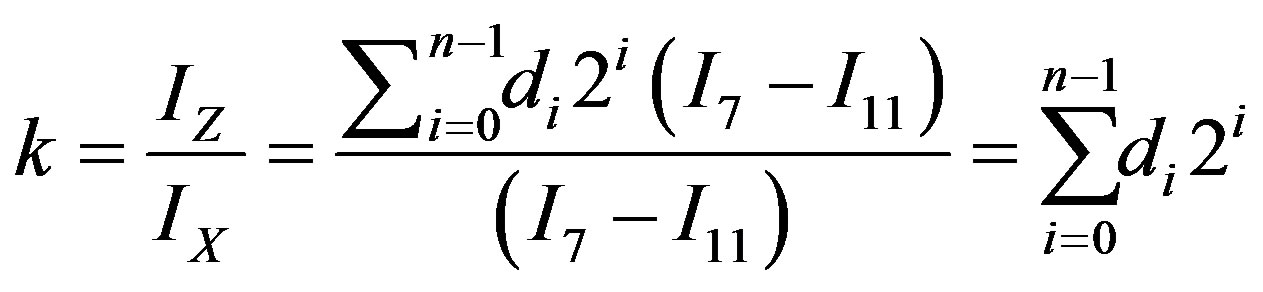 (11)
(11)
where di represents the bits applied to the i-th branch in the CSN. Now depending upon its value, whether it’s a logic 1 or logic 0, the current is enabled or disabled to flow in that particular branch [13-15].
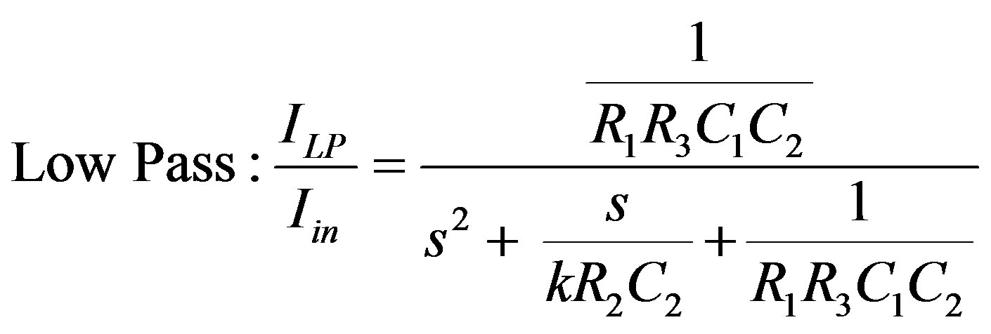
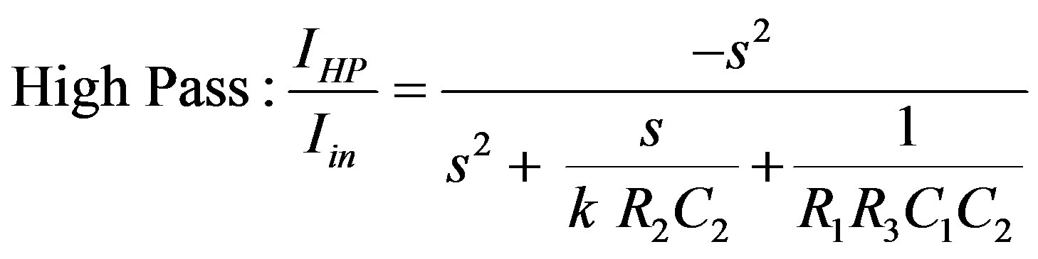
5. Digitally Programmable Multifunctional Filter
In this section, the voltage-mode multifunctional biquadratic filter of Figure 3 is digitally programmed by using a Current Summing Network (CSN) with electronic control of quality factor as shown in Figure 7. The introduc-
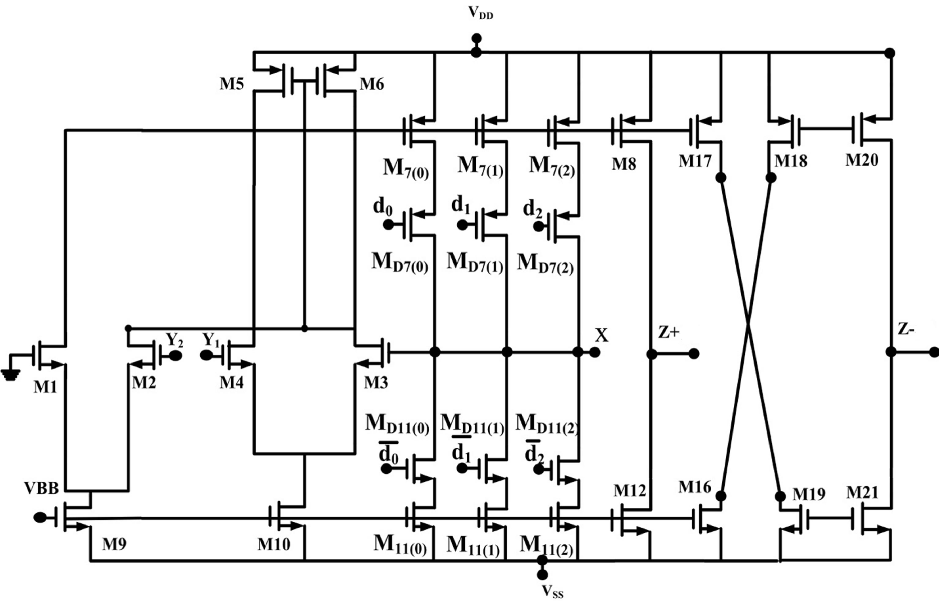
Figure 6. CMOS realization of the digitally programmable DVCC with gain k [12].

Figure 7. Digitally controlled current-mode biquadratic filter.
tion of the digital control module, comprising of CSN leads to a significant change in the expression of the transfer function of multifunctional filter. The expression for the digitally programmable filter functions can now be expressed as:
 (12)
(12)
 (13)
(13)
 (14)
(14)
 (15)
(15)
The resonant angular frequency, ωo and the quality factor, Q, are given by:
 (16)
(16)
 (17)
(17)
where
 (18)
(18)
where di represents the bits applied to the i-th branch in the Current Summing Network (CSN).
It can be seen from Equations (16) and (17) that only the expression of quality factor is varying with control word, whereas the cut-off frequency is independent of it. Since quality factor indicates the selectivity characteristic of a filter and it’s significance is more with the band pass, as compared to the other filters, so for this digitally controlled circuit focus will be only on the response of band pass filter.Moreover, the circuit utilizes grounded capacitors for the filter’s realization, which makes it suitable for integrated circuit implementation.
6. Simulation Results
The proposed digitally controllable multifunctional voltage mode filter has been simulated and all the realizations are designed and verified using PSPICE simulation tool with good results in support of the theory to ensure that the expected functionality is indeed obtained. The CMOS implementation of Digitally Programmable DVCC is shown in Figure 7 and it employs TSMC 0.25 μm CMOS technology process parameters. Figures 8-10 show resultant waveforms of Band Pass Filter for control word [0 0 1], [1 0 1] and [1 1 1] respectively by setting the associated bits to either logic1 or logic 0, where each bit corresponds to a particular binary weight. Furthermore, Figures 11 and 12 illustrate the variation in quality factor and resonant frequency with different control words. Theoretically, the quality factor of digitally controlled band pass filter has a linear relationship with control word, as indicated by Equation (17) and the same is verified with the help of PSPICE simulations, summarized in the form of a graph, shown in Figure 10. The quality factor of the band pass filter is found to vary from 1.01 to 6.33 and resonant frequency is almost constant all
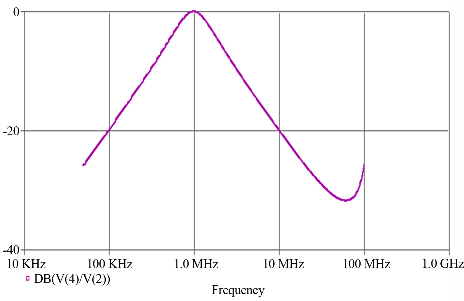
Figure 8. Simulated magnitude response of band pass filter with control word [d2 d1 d0 = 0 0 1] selected Q = 1, fo = 1 MHz.
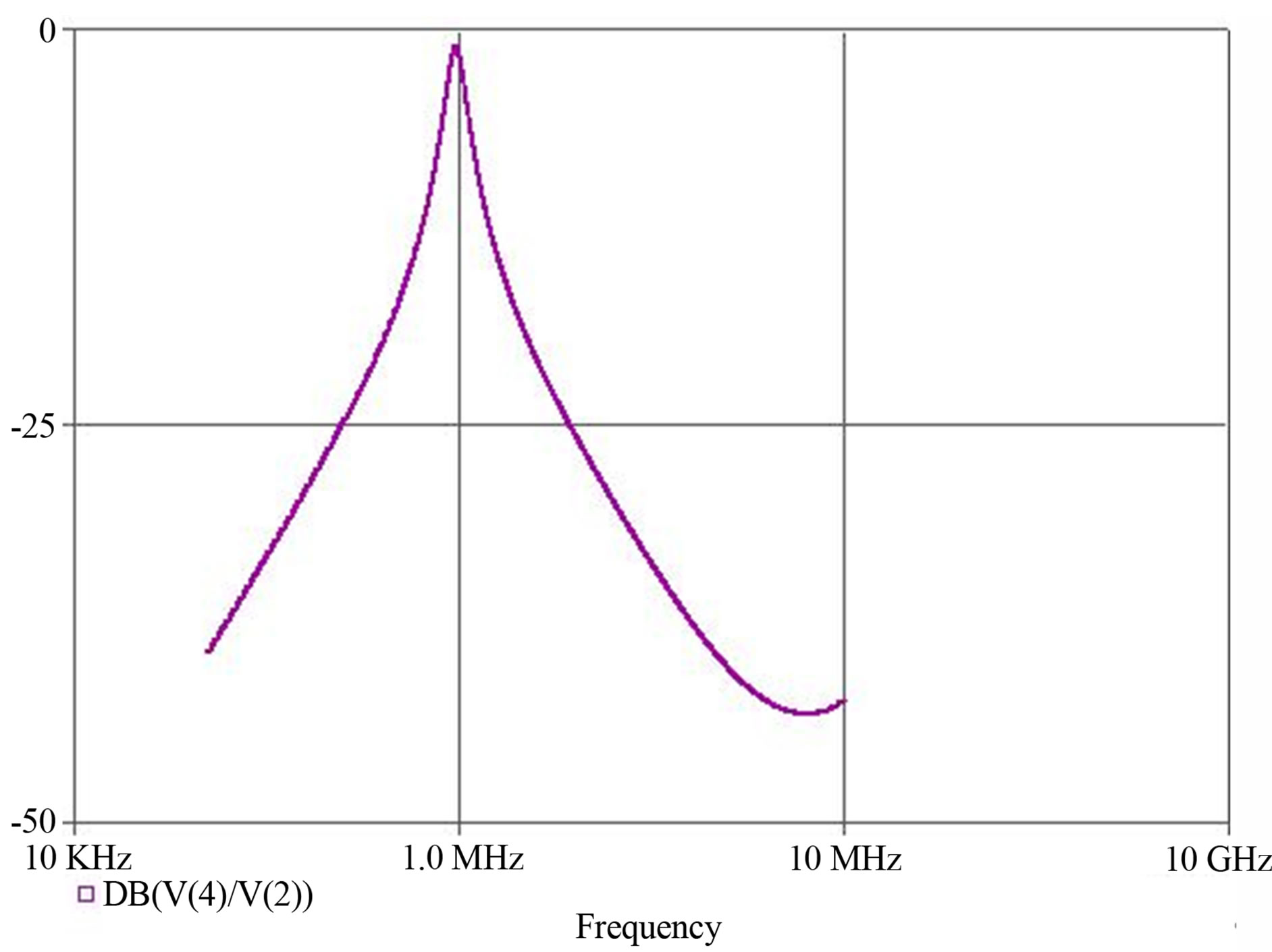
Figure 9. Simulated magnitude response of band pass filter with control word [d2 d1 d0 = 1 0 1] selected Q = 4.23, fo = 1 MHz.
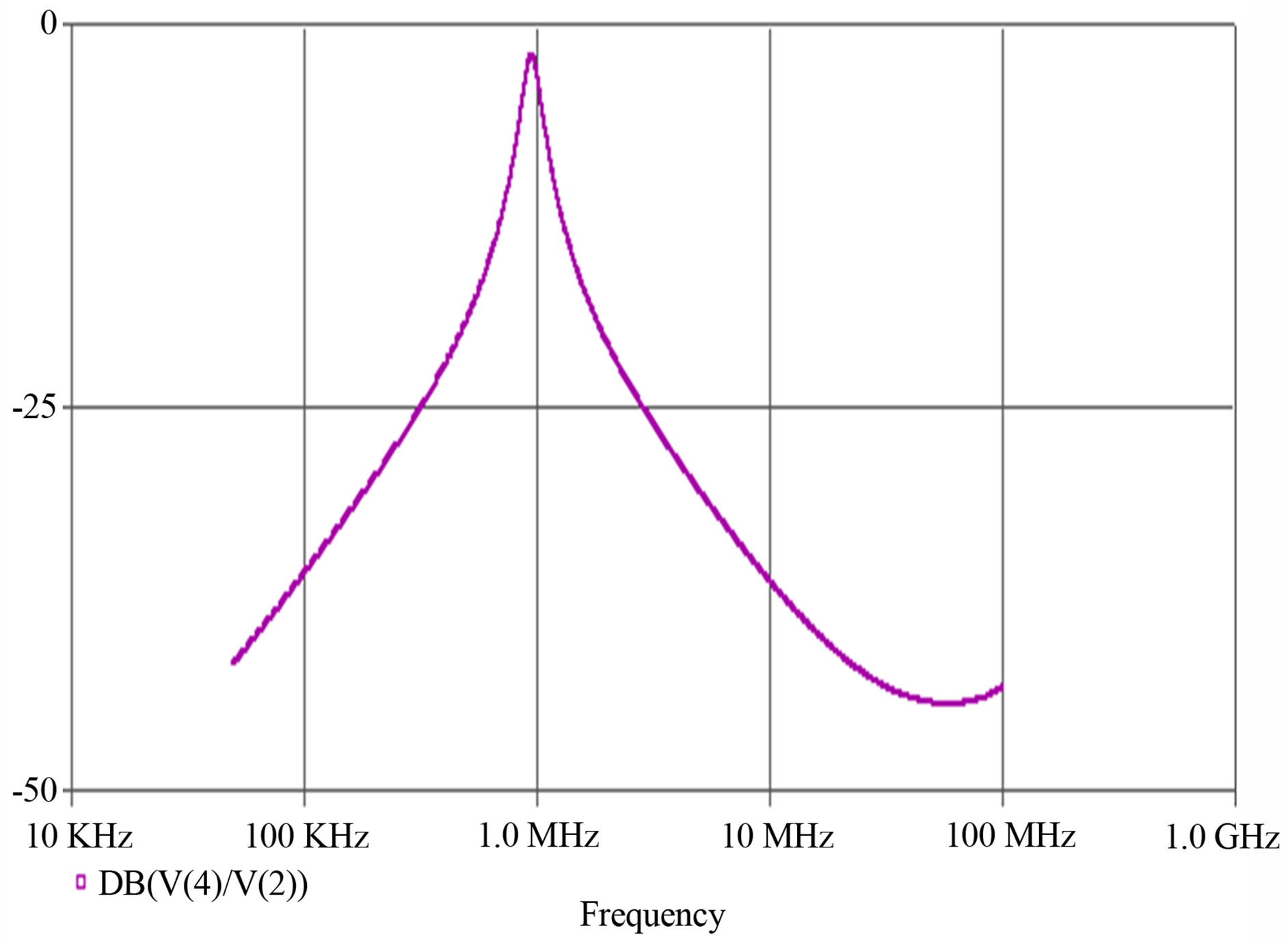
Figure 10. Simulated magnitude response of band pass filter with control word [d2 d1 d0 = 1 1 1] selected Q = 6.13, fo =1 MHz.
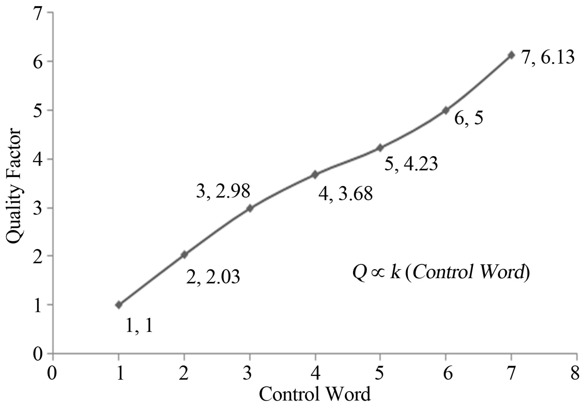
Figure 11. Variation (linear) of quality factor with digital control word.
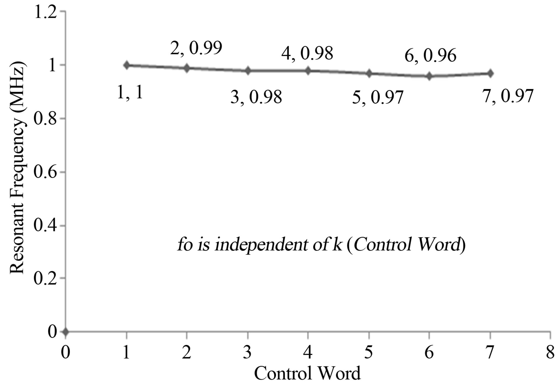
Figure 12. Variation (constant) of resonant frequency with digital control word.
the plots are in excellent mathematical conformity with the transfer functions given in equations. The slight decrease in the resonant frequency is because of the nonideal effects. The performance of the DVCC generally deviates from the ideal behavior since, the voltage and current conveying actions are not exact, therefore leading to slight degradation in performance of the circuit realized using these active elements. In order to account for these non ideal effects, the parameters of α and β are introduced, where α accounts for current transfer gains and β accounts for voltage transfer gains. These transfer gains differ from unity, by the voltage and current tracking errors of the DVCC.
The Digitally Programmed Multifunctional filter can be controlled by a 3-bit control word that can be varied from 1 to 8. However in order to achieve more variation in the Q-factor of the circuit, the digital control word could be increased by adding more transistor pairs in the current summing network of digitally controlled DVCC.
7. Conclusion
In this paper, a novel digitally controllable voltage-mode universal biquadratic filter based on DVCC was presented. Digital tuning has been achieved by the variation of 3-bit digital control word. PSPICE simulations were carried out to ascertain the working of the proposed filters and the results were found to match with the theoretical results.
REFERENCES
- B. Wilson, “Recent Developments in Current Conveyors and Current-Mode Circuits,” IEE Proceedings Pt. G, Vol. 137, 1990, pp. 63-77.
- A. Sedra and K. C. Smith, “A Second Generation Current Conveyor and Its Applications,” IEEE Transactions, Vol. CT-17, 1970, pp. 132-134.
- A. M. Soliman, “Low Voltage Wide Range CMOS Differential Voltage Current Conveyor and Its Applications,” Contemporary Engineering Sciences, Vol. 1, No. 3, 2008, p. 105.
- H. O. Elwan and A. M. Soliman, “Novel CMOS Differential Voltage Current Conveyor and Its Application,” IEEE Proceedings of Circuits Devices System, Vol. 144, 1997, pp. 195-200.
- H. Sedef and C. Acar, “A New Floating Inductor Circuit Using Differential Voltage Current Conveyors,” Frequenz, Vol. 54, No. 5-6, 2000, pp. 123-125. http://dx.doi.org/10.1515/FREQ.2000.54.5-6.123
- H. Sedef and C. Acar, “A New Floating FDNR Circuit Using Differential Voltage Current Conveyors,” International Journal of Electronics and Communications, AEÜ, Vol. 54, 2000, pp. 297-301.
- S. S. Gupta and R. Senani, “Grounded Capacitor Current Mode SRCO, Novel Application of DVCCC,” Electronics Letters, Vol. 36, No. 3, 2000, pp. 195-196. http://dx.doi.org/10.1049/el:20000240
- T. Dostal, D. Biolek and K. Vrba, “Adjoint Voltage Current Mode Transformation for Circuits Based on Modern Current Conveyors,” Fourth IEEE International Caracas Conference on Devices, Circuits and Systems, Aruba, 17-19 April 2002.
- S. Minaei and Ç. Temizyürek, “Dual Input All-Pass Filter Using DVCC,” International Symposium on Signals, Circuits & Systems (SCS), Iasi, 10-11 July 2003.
- H. Chen, Y. Lin, W. H. Wu and C. Li, “Versatile DVCCBased Universal Voltage-Mode Biquadratic Filter,” Progress in Electromagnetics Research Symposium Proceedings, Suzhou, 12-16 September 2011.
- S. A. Mahmoud, M. A. Hashiesh and A. M. Soliman, “Low-Voltage Digitally Controlled Fully Differential Current Conveyor,” IEEE Transactions on Circuits and Systems-I, Vol. 52, No. 10, 2005, pp. 2055-2064.
- W. Y. Chiu, J. W. Horng, H. Lee and C. C. Huang, “DVCCBased Voltage-Mode Biquadratic Filter with High-Input Impedance,” 5th IEEE International Symposium on Electronic Design, Test & Applications, Ho Chi Minh, 13-15 January 2010, pp. 121-125.
- S. Minaei and E. Yuce, “All-Grounded Passive Elements Voltage-Mode DVCC-Based Universal Filters,” Circuit, Systems, and Signal Processing, Vol. 29, No. 2, 2010, p. 295.
- H. P. Chen and S. S. Shen, “A Versatile Universal Capacitors-Grounded Voltage-Mode Filter Using DVCCs,” Electronics and Telecommunications Research Institute Journal (ETRI), Vol. 29, No. 4, 2007, pp. 470-475.
- T. Tsukutani, Y. Sumi and N. Yabuki, “Novel Currentmode Biquadratic Circuit Using Only Plus Type DODVCCs and Grounded Passive Components,” International Journal of Electronics, Vol. 94, No. 12, 2007, pp. 1137-1146. http://dx.doi.org/10.1080/00207210701791085