Circuits and Systems
Vol. 4 No. 2 (2013) , Article ID: 29844 , 14 pages DOI:10.4236/cs.2013.42018
Graph Modeling for Static Timing Analysis at Transistor Level in Nano-Scale CMOS Circuits*
1Computer Engineering Department, Jordan University of Science and Technology, Irbid, Jordan
2Information Technology Department, Balqa’ Applied University, Irbid, Jordan
Email: #abdoul@just.edu.jo
Copyright © 2013 Abdoul Rjoub et al. This is an open access article distributed under the Creative Commons Attribution License, which permits unrestricted use, distribution, and reproduction in any medium, provided the original work is properly cited.
Received November 6, 2012; revised December 7, 2012; accepted December 14, 2012
Keywords: Critical Path Estimation; Graph Models; MOSFETs; Sequential Circuits; Transistor Level; Static Timing Analysis
ABSTRACT
The development and the revolution of nanotechnology require more and effective methods to accurately estimating the timing analysis for any CMOS transistor level circuit. Many researches attempted to resolve the timing analysis, but the best method found till the moment is the Static Timing Analysis (STA). It is considered the best solution because of its accuracy and fast run time. Transistor level models are mandatory required for the best estimating methods, since these take into consideration all analysis scenarios to overcome problems of multiple-input switching, false paths and high stacks that are found in classic CMOS gates. In this paper, transistor level graph model is proposed to describe the behavior of CMOS circuits under predictive Nanotechnology SPICE parameters. This model represents the transistor in the CMOS circuit as nodes in the graph regardless of its positions in the gates to accurately estimating the timing analysis rather than inaccurate estimating which caused by the false paths at the gate level. Accurate static timing analysis is estimated using the model proposed in this paper. Building on the proposed model and the graph theory concepts, new algorithms are proposed and simulated to compute transistor timing analysis using RC model. Simulation results show the validity of the proposed graph model and its algorithms by using predictive Nano-Technology SPICE parameters for the tested technology. An important and effective extension has been achieved in this paper for a one that was published in international conference.
1. Introduction
The revolution from the micro-technology to nano-technology and the growing demand on high performance VLSI chips drive industry companies like Intel and IBM to have their own internal tools. These tools are used to estimate CMOS circuit static timing analysis at transistor level in order to design VLSI chips with the best performance [1].
Static Timing Analysis (STA) technique is commonly used in VLSI design. It is characterized as very fast analysis compared to dynamic circuit simulation like (HSPICE, Montecito…), that’s because it does not require any test vectors. It calculates approximately the gate delay using look-up table or linear equations. However, existing delay models become less accurate in nanometer circuits, because of the growing interactions between nodes [2].
The optimization objectives for designing VLSI circuits are the power dissipation, area cost, and circuit delay [3]. The hot research field concentrates on how much delay could be increased for the circuit to save more power and area; this is done by finding the accurate timing analysis of the CMOS circuits and adding some delay to the noncritical path nodes in order to improve the circuit power dissipation without degrading the circuit performance.
From a timing view, critical path nodes are the nodes, which have delay cannot be increased. On the other hand, non-critical path nodes are the nodes which their delay can be increased. This amount of increase is called the slack time, thus the slack time for critical path nodes equal zero and the noncritical path nodes have positive values for their slacks [4]. To find the slack time for every element in CMOS circuit, all timing parameters for that circuit should be calculated. These parameters are circuit frequency, delay, arrival, and required times for every node in the circuit.
At transistor level, the slack time for transistors in any CMOS circuit is the maximum value of delay which can be increased without violating the circuit performance [3], thus the optimum decrease in the area or in power can be calculated exactly to fill and exploit the slack time of the non-critical path transistors [5].
Various approaches have been suggested in the past for estimating the slack time. One of the techniques which designed for slack time calculation in combinational circuits is Zero-Slack Algorithm (ZSA) [6]. It’s an improved version of an efficient technique proposed in [7,8]. The main drawback of this technique is that it does not give accurate estimation for the circuit critical path or subcritical paths. This is because the estimation is done at gate level rather than transistor level. Also, this technique does not calculate the delay of the gates simultaneously. It is using pre-defined look-up table to store the delay of gates, so any change in the circuit transistors parameters needs to update this look-up table. Also, this technique just targets the combinational circuits and ignores the sequential circuits.
The potential slack-time technique [3] was proposed as a very effective metric that measures the combinational circuit performance. In this technique, the delay of gates is calculated by using linear equation. But, this technique cannot be applied on large circuits (thousands of transistors) [9]. Also the circuits must be converted from the transistor level to the gate level. The second drawback of this technique is that it does not calculate a delay of transistors’ interconnection, which is becomes important in new technologies. Finally, the potential slack-time technique just targets the combinational circuit and ignores the sequential circuits.
The most important timing parameters for any circuit are the delay parameters of the circuit. A variety approaches and techniques were used in the past to estimate the delay timing for optimization purposes. In [10,11], they used simple linear-resistor delay models for transistors in order to optimize the design. In [12], they also use an RC-model to estimate the delay, and then they solve the resulting non-linear equations by an iterative relaxation technique to optimize the design. In [13], the delay modeling is based on pre-characterization of the effective transition-resistances model. Such methods are time and space consuming and incorporate interpolation errors, also they are old and don’t accurate for nano-technology parameters because of the development from Micro to Nano dimensions. Additionally, they target only the combinational circuits.
All the approaches that are mentioned have two problems: firstly, the circuits must be converted from transistor level to the gate level, where some circuits for example (memory cells, some full adders) are difficult to convert. Secondly, the gate delay calculation [14], this is because the extracted gates are limited to a few fixed structures and transistor sizes, where it is not feasible to create a delay model for every gate [14]. One way to overcome these problems is by building a transistor graph model. In this model, each transistor is presented individually, by this way; results should be more accurate and more precious, which it is the main target of this paper.
Circuit transformation from gate level to a graph model, which has vertices and edges to represent the gates and the connections, is straightforward. While, by going more deep, transform the same circuit to a graph from the transistor level instead of gate level is very complicated. That’s because the vertices of the graph aren’t gates, they are PMOS and NMOS transistors and the edges are the connection between the transistors terminals either source or drain or gate.
In VLSI circuit design, the delay time, silicon area and power dissipation are the essential parameters to optimize the performance of digital circuit [9]. It is known that the relation between the performance from one side as well as the silicon area and power dissipation from other side is reversed [15]. Thus, any increase in the frequency causes an increase in the power dissipation. As a result, it becomes a demand to look for new techniques that increase the operation without any scarifying the power dissipation. This could be happened if different low power design techniques are suggested and applied at transistor level [15].
In this work, clear and explained methods to find the critical time, frequency (CLOCK time), the slack and timing constraints at transistor level are proposed in order to find an effective way for estimating timing analysis of any circuit, and building a tool with clear algorithms and methods for researchers to perform static timing analysis job.
The Graph transformation and the timing analyzer in the tool incorporate accurate analytical models and equations to describe the behavior of the transistors at Nano dimensions in the circuit, the delay and capacitance equations for a transistor, which is built in the timing analyzer tool, are extracted from BSIM 4.1 which addresses the MOSFET transistors at nano-technology [16].
In this paper, a Graph model transformation algorithm, which is built inside a tool, is introduced to find the critical path of any CMOS circuit and the timing analysis using the timing analyzer. The timing analyzer depends on the transformation of the CMOS transistors in any circuit to a Graph model. Thus, based on this timing analyzer, the critical and CLOCK time are calculated depending on delay time of transistors, which are involved in the critical path, the sequential elements in the circuit also are analyzed to calculate their timing parameters. The proposed algorithm calculates also the slack and arrival times for each transistor in the circuit. It is also capable to show the effects of changing the sizing of the transistors that are located in the non-critical path in saving the leakage power for the circuit.
The paper is organized as followed. Background of timing parameters is shown in Section 2. Section 3 discusses the characteristics of the proposed graphs and algorithm in details. In Section 4, an example based on bench mark was run based on the proposed algorithm. Finally, Section 5 shows the conclusion.
2. Background and Definitions
From the 1990s, static timing analysis (STA) became the dominant simulation method for VLSI designs. STA used at the bottom layer of many optimization tools used for VLSI simulations and design. STA differs from the input vector simulation; it is easier and has greater simulation speed with almost the same accuracy [17].
In Static Timing Analysis (STA), the modeling of the delay time has always focused on models that represent gates as black boxes, without calculating the accurate internal waveforms. The STA calculates the gate delay approximately using look-up table and equations include the transistors sizes, the load capacitance and input ramps [2]. Most models in literature fall into this category. However, even the most advanced cells libraries do not have universal high accuracy for all types of gates.
Clearly, a modeling and analysis approach that is accurate within a few percent of SPICE is required for all gate types and arcs. This approach should also be fast enough for practical timing and noise analysis on multimillion gate designs. One way to overcome this problem is to move down to the transistor level and model each transistor individually which is the main target of this work. In order to have accurate results, the delay time is calculated using accurate equations in terms of transistor size, load capacitance and the SPICE parameters based on Nano-scale technology.
The maximum operating speed of a circuit which is the critical time of that circuit is limited by the signal propagation delay along the critical path. Thus the critical time of a sequential circuit is the global CLOCK of that circuit, clock is calculated by the summation of all transistors delay time along the critical path of the combinational sub circuits, with sequential elements setup and clock-toQ timings.
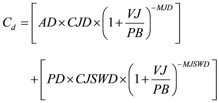
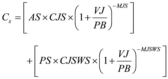
Each transistor has three practical capacitances: the gate Cg, the drain Cd and the source Cs capacitances. Cd and Cs are not depending on state of transistor and its values are constant for all transistor states. Cd and Cs are calculated by BSIM4 Equations (1) and (2) respectively in terms of transistor size and the SPICE parameters [16].
 (1)
(1)
 (2)
(2)
Where: AD, AS, PD and PS are area of the drain, area of the source, periphery of the drain and periphery of the source respectively. These parameters which represent sizes of a transistor are obtained from the circuit netlist file. The other parameters are SPICE parameters and depend on the technology that is used to build the circuit. These parameters are obtained from the technology model-card.
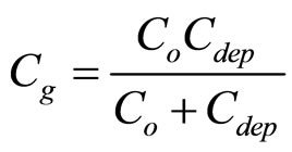
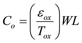
Calculation of Cg is more complicated because it depends on transistor state. This capacitance consists of two series capacitances; the gate oxide capacitance Co and the depletion capacitance Cdep as given by Equation (3). Co depends on area of a transistor channel (WL) and gate oxide thickness Tox and it does not depend on transistor’s state of operation as shown in Equation (4), where W and L are the transistor channel width and length respectively.
 (3)
(3)
 (4)
(4)
Cdep depends essentially on transistor’s state of operation because it is changing with value of Vgs as shown in Equation (4), where Xdep is the depletion layer and given by Equation (4).
 (5)
(5)
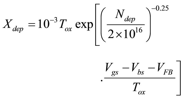 (6)
(6)
Where:
Ndep is channel doping concentration;
Vgs is voltage difference between the transistor source and gate;
Vbs is voltage difference between the transistor source and bulk;
VFB is flat band voltage of the transistor.
In saturation state the value of Cdep is precious and affects on value of Cg, while in linear state the value of Cdep is very large where Xdep goes to zero, where in this case value of Cdep can be ignored [16], and as a result Cg ≈ Co. Thus, two Cg values are calculated; one when the transistor in saturation state by Equation (3) and another when the transistor in linear state by Equation (4) all of these equations are obtained from BSIM4 [16].
The delay time of a transistor is dependant largely on the load capacitance of its drain, supply voltage, type and slope of driving signals. Load capacitance equals summation of its drain capacitance, capacitance of wires that connects its drain with other transistors in the circuit, and the capacitances of the other transistors that are connected with its drain. The capacitance of the wires depends on the material of the wires, its thickness, width and length.
The transistor’s load capacitance is used to calculate the delay time. To calculate the delay time, RC model are used in term of transistor size and the SPICE parameters [16]. The sizes of a transistor are obtained from the circuit netlist file, while the SPICE parameters are obtained from the technology model-card. The Equations (7) and (8) are used to calculate falling and rising delay times for the CMOS transistor, respectively. The fall time is related to the NMOS, while the rise time is related to the PMOS transistor. The falling time delay is given by [16]:
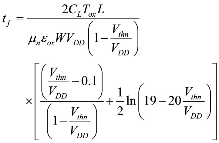 (7)
(7)
Where:
CL is the transistor load capacitance;
Tox is the gate oxide thickness;
L is the transistor channel length;
μn is effective surface mobility of the electrons in the channel;
εox is the permittivity of silicon oxide;
W is the transistor channel width;
VDD is the supply voltages;
Vthn is the NMOS transistor threshold voltages.
The rising delay time is given by [16]:
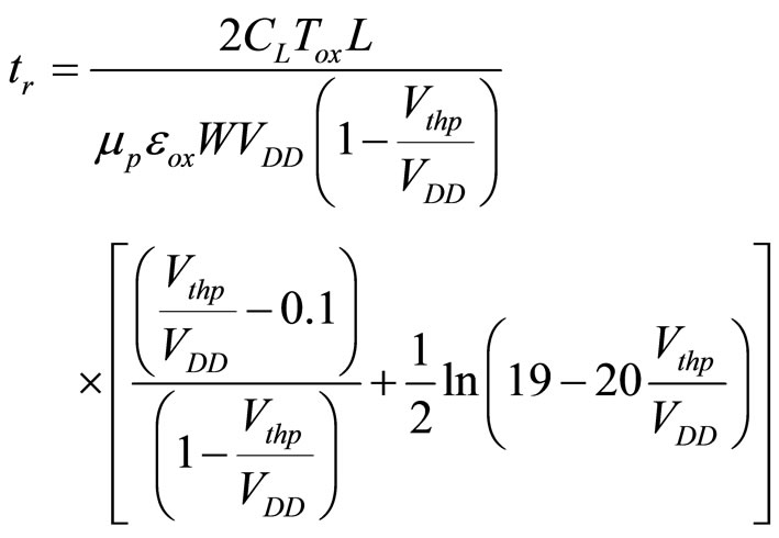 (8)
(8)
Where:
μp is effective surface mobility of the holes in the channel;
Vthp is the PMOS transistor threshold voltages.
The effective surface mobility is technology parameter equals 0.032, 0.0128 for electrons and holes respectively. Vth is a core parameter in the delay equations, and it is related to the thickness of the gate oxide.
In real circuits, the task of calculating the minimum clock period of sequential circuit is computed by finding the longest combinational path between any two flipflops of the circuit and summing setup-time, flip-flop delay to it with neglecting the clock skew and jitter [18]. The sequential elements value is changed according to the input value with respect to the change at the edge of the CLOCK, any flip-flop is sensitive either for rising or falling edges of clock [4]. Any sequential elements have the following timing parameters [19]: Propagation delay (tClk-Q), Contamination delay (tcd), Setup time (ts), and Hold time (th).
3. Proposed Graph Models and Algorithm
In this paper, the simulator transforms the CMOS circuit from transistor level into a Graph model G (V, E). This graph is cyclic graph for sequential circuits. Many papers [20-22] talked about acyclic graph for combinational circuits. This paper, additionally work at transistor level with nano dimensions, it targets the sequential and combinational circuits, which is very dominant in CMOS circuits. In addition, there is no more research papers in the literature deal with time analysis for sequential circuits, those papers also do not deal with nano-scale SPICE parameters [20-22].
Because of the importance of the capacitances which affects the transistor delay time, a capacitance graph will be built to estimate every transistor capacitances, which is used in the timing analyzer.
In this paper, two graphs are proposed; the first graph is Load Capacitance Graph (Gc), which is proposed to calculate the load capacitance and the delay of each transistor in the circuit. The another graph is Timing Analysis Graph (GT), which is proposed to present propagation of signals in the circuit and to calculate the circuit timing constraints such as arrival, required and slack times, as shown in Figure 1.
3.1. Load Capacitance Graph (Gc)
The Gc is direct graph consist from set of vertices Vc and set of edges Ec, where every vertex v in Vc represents a transistor and has its type and index. Every edge e in Ec represents wire connection between two transistors, and has a weight related to its capacitance. In order to build Gc, the flowing procedure is proposed.
• Every transistor in the circuit is represented by vertex in Vc.
• If the drain of transistor (A) is connected to the source of transistor (B), then a direct edge should be added from vertex A to vertex B in Gc.
• If the drain of transistor (A) is connected to the gate of transistor (B), then a direct edge should be added from vertex (A) to vertex (B) in Gc.
• If the drain of transistor (A) is connected to the drain of transistor (B), then two direct edges should be added: The first one from vertex A to Vertex B, and another one from Vertex B to vertex A.
To manipulate this procedure the GCG algorithm is proposed, this algorithm reads HSPICE Netlist file as ASCII Code, then it calculates Cg, Cd and Cs capacitances for all transistors in the circuit by using BSIM4 equations, and finally, it generates the Gc graph. A transistor dimensions are read from the circuit Netlist file, while the technology parameters are extracted from technology modelcard (technology file). Figure 2 shows the GCG algorithm
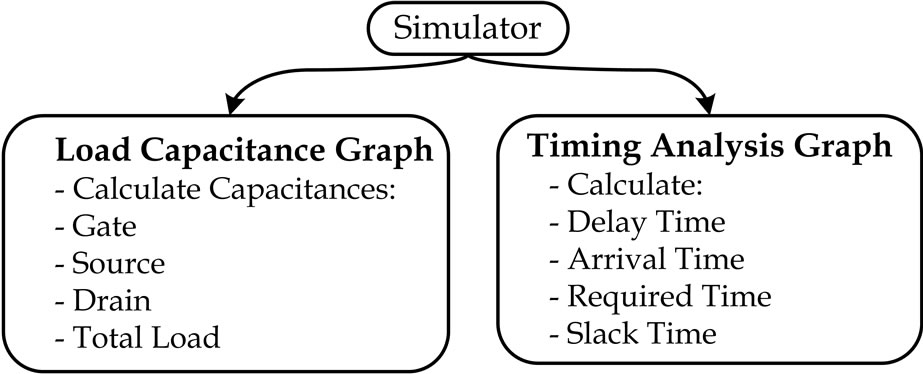
Figure 1. Simulator block diagram.
pseudo code.
Applying this algorithm onto 2 Input AND gate that is shown in Figure 3, will be generated Gc that is shown in Figure 4.
As mention before, the purpose of Gc graph is to calculate the load capacitance CL for each vertex in Gc. This could be achieved by tracing the outgoing edges form the vertex in Gc, and summing weights of these outgoing edges with capacitances of destination vertices. Figure 5 shows LCC algorithm which is proposed to calculate the CL for each vertex in Vc.
In this algorithm, each vertex v in Vc has variable vCL to store load capacitance value, the drain capacitance of v (vCdrain) is stored in vCL at the beginning (Line 2), and then the all outgoing edges of v are traced in order to find the destination vertices. Then the outgoing edges weights and terminal capacitances of destination vertices are added to vCL. Giving an example, if such edge e connects v with source of other vertex w (Line 11), then the weight of e (eC) and the source capacitance of w (wCsource) are added to vCL (Line 12), The same scenario is done if e connects v with drain of w (Line 13), which in this case (wCdrain) and (eC) are added to vCL (Line 13).
As shown in Figure 5, the algorithm has different scenarios if e connects v with gate of w (Line 4), because the transistor have two values for gate capacitance as mention previously, one when the transistor in linear state (Cgate_on) and the other when the transistor in saturation state (Cgate_off). In this case, the algorithm checks the w; if v and w have same type (ex. N type) (Line 5), then (wCgate_off) and (eC) are added to vCL because the transistor w is explicitly must be in saturation state (Line 6), otherwise if v and w have different types (Line 8), then (wCgate_on) and (eC) are added to vCL, where the transistor w must be in linear state in this case (Line 9).
After Appling this algorithm on Gc, the purpose of Gc is gained and the CL is calculated for every transistor in the input circuit. Table 1 shows CL for 2_input AND gate.
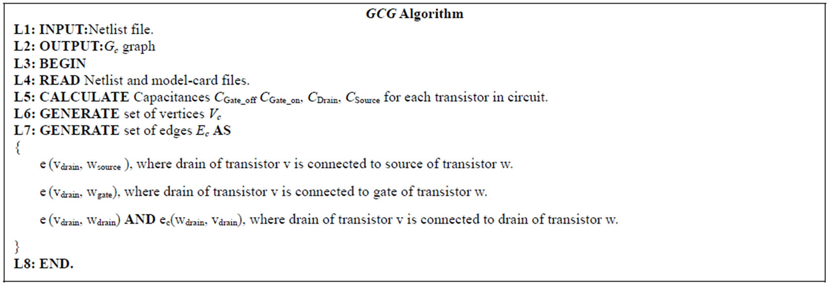
Figure 2. GCG algorithm of Gc graph generation.
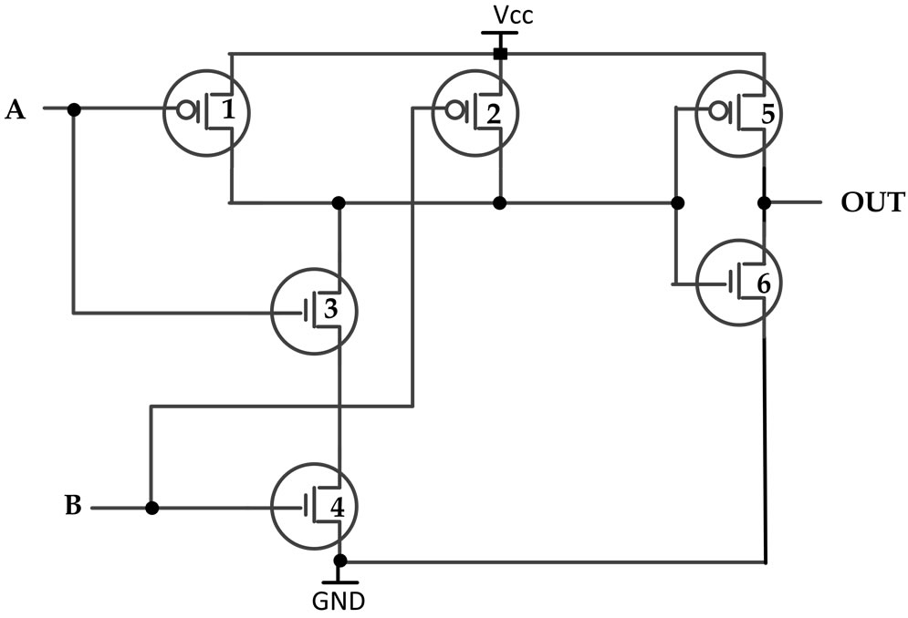
Figure 3. Conventional CMOS AND gate.
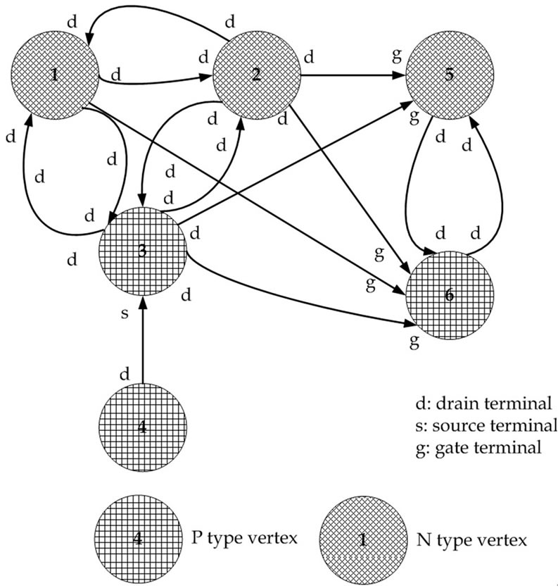
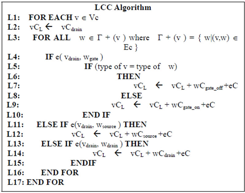
Figure 5. LCC algorithm for CL calculation.
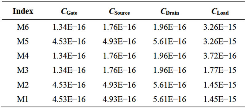
Table 1. Total capacitances for 2_Input AND gate.
At the end of Capacitance Graph creation, CL is already found and calculated for every transistor (vertex) in the circuit. There is no difference here between combinational or sequential because the rules are clear and the feedback existence doesn’t affect the algorithm. In capacitance calculation, the algorithm ignores the linear capacitances for transistor’s gates, thus for simplicity it uses the saturation and cut-off capacitances.
3.2. Timing Analysis Graph (GT)
Timing Analysis Graph (GT) is responsible for estimating the timing analysis for any CMOS circuit to deliver a static timing analysis, and exploiting the slack time for power and area optimization. Timing Graph has also transistors represented by vertices and wire connections represented by edges GT (V, E), the CMOS circuit is transformed from its view to Graph model to show the propagation of signal from the inputs to the outputs through the circuit itself.
The function of Timing Analysis Graph (GT) is to present the paths of signals in the circuit. The path is a sequence of distinct transistors, which begins with one of the inputs, and ends with one of the outputs, where at certain input; all of these transistors are turned on. The delay path is the summation of each transistor’s delay in that path. The signal goes in transistor from its gate or source and moves out from its drain. In most cases, the signal moves through the circuit in alternating sequence from drain of PMOS transistor to the gate of NMOS transistor and from drain of NMOS transistor to the gate of PMOS and so on. While in other cases, the signal goes through the circuit in constant sequence from drain of PMOS transistor to source of PMOS transistor and from drain of NMOS transistor to source of NMOS.
The timing analysis graph GT = (VT, ET) is a spanning sub-Graph of GC, where all the vertices of VC are presented in VT, and ET is a subset of EC, in order to generate GT from Gc, the flowing procedure is followed:
All incoming edges to the drain terminals are removed.
All incoming edges to the gate terminal that come from the similar vertex type are removed.
To identify the starting points of the paths, an extra set of vertices VIN is added to GT in order to represent the circuit input terminals where all paths are started from. Also, a new set of vertices Vout is added to identify the end points of the path. Vfeedback vertices is used to represent the feedback in sequential circuits, which returns from flip-flops output. Figure 6 shows GTG algorithm, which is proposed to generate GT.
By the end of Timing Graph GT creation, timing analysis of the circuit are ready, this happens step by step starting with copying Gc and removing the unnecessary edges from it as shown at L4-L9. At L10-L13, input, output, and feedback vertices are created and linked with the inputs or the outputs or flip-flops of transistors connected with as in the original circuit, as shown at L13-L21. Then the propagation delay for every transistor is calculated by the tool depending on the delay equations at BSIM as shown at L22-L24.
At L25-L27, all flip-flops timing parameters like tC-Q, tsetup, and thold times are calculated depending on the delay of transistors in the flip-flops itself. These timing parameters are formed by the delay of specific transistors in
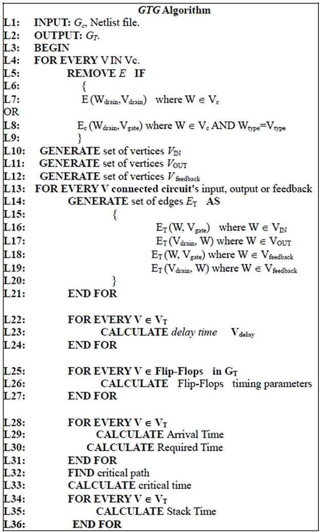
Figure 6. GTG algorithm for GT generate.
the flip-flop, some transistors affects only setup time, some affects the tC-Q and setup.
Depending on the delay for transistors in the combinational sub-circuits and using the Timing Graph GT, critical time and critical path are found, as shown at L32-L33. Finally at L34-L36, transistors slack times are computed. The Figure 7 show GT graph of AND gate that is shown in Figure 3.
Each vertex in the GT has a weight associated with the delay of the corresponding transistor. Therefore, to calculate vertices’ weights (delay), RC model are used, the falling time equation is used to calculate the weights of NMOS vertices, and the rising time equation is used to calculate the weights of PMOS vertices. While the weights of the input and output vertices are set to zero because they haven’t delay.
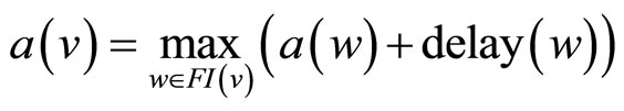
The arrival time of a vertex a(v) is defined as the delay of the longest path between that vertex and any of input vertices in the graph. The arrival time of the input vertices a(VIN) are zero. The arrival time for the flip-flop block is the summation of the arrival time of previous transistors and their delay. The arrival time of any vertex v in GT a(v) is calculated by using the well Known recursion formula:
 (9)
(9)
Where FI(v) is the set of fan-ins of vertex v.
The required time is defined as the delay of the longest path between that vertex fan-out and any of output vertices in the graph.
The required time of the output vertices are the critical time. The required time for a flip-flop is the flip-flop setup time subtracted from the CLOCK of the circuit. The required time of any vertex v is calculated by using the well known recursion formula as shown in (10).
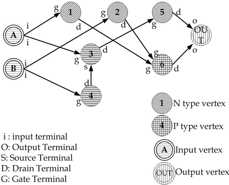
Figure 7. GT graph of CMOS AND gate.
 (10)
(10)
Where FO(v) is the set of fan-outs of vertex v.
For all w vertices are fan out of v, the required time for flip-flop as block is:
 (11)
(11)
The critical delay Dcritical which is the delay of the longest path in GT equals to the maximum arrival time between all output vertices.
 (12)
(12)
The slack time of a vertex s(v) is defined as the period of time that can be added to vertex delay without affecting the graph critical delay. The slack time of vertex v is the time deference between the critical delay and the delay of the longest path that this vertex v involved in. In order to calculate the slack time, the following equation is used:
 (13)
(13)
Flip-flops slack time shows up in two places, thus every flip-flop as a block has a slack time in its input and output. The slack input is also shown up at high or low values, which produced from the NMOS and PMOS transistors inside the flip-flop, thus every flip-flop vertex have:
Slack time at D input when D signal transits from high to low:
 (14)
(14)
Slack time at D input when D signal transits from low to high:
 (15)
(15)
Slack time at Q output when Q signal transits from high to low:
 (16)
(16)
where v is fan-out(ff) and v is PMOS transistor either there is feed back or not.
Slack time at Q output when Q signal transits from low to high:
 (17)
(17)
where v is fan-out(ff) and v is NMOS transistor either there is feed back or not.
Slack time is a positive value, and the slack time of any vertex that joins the critical path must be zero. Table 2 illustrates the arrival time, the required time, and the slack time for AND gate as example as shown above.
In this example, each vertex has its own delay, vertices M3, M4, and M5 are located in the critical path and the delay of critical path is 5.136e−012 Sec This value is the
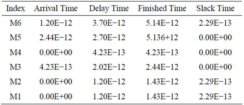
Table 2. Total timing analysis for AND circuit.
maximum arrival time for the output vertices according to our assumptions based on a specific width.
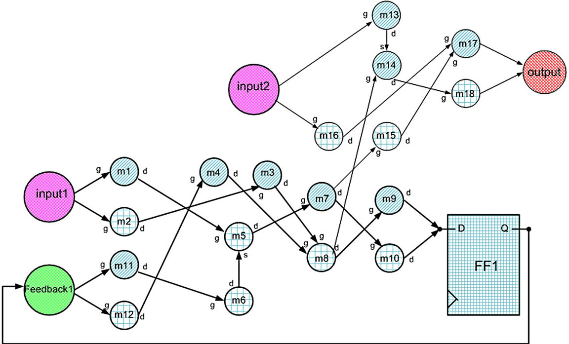
Figure 8 shows a sequential circuit that contains 18 transistors, which forms the combinational sub-circuit. Also, it contains 1 flip-flop, which contains 26 CMOS transistors, two inputs, one output, and one feedback from the flip-flop.
In real circuits, flip-flops actually are consisted from 26 CMOS transistors. In this work, flip-flops are analyzed first at transistor level, and then they will be converted to a block entity, which has its new timing parameters. Figure 9 shows the Timing graph GT for the test circuit shown in Figure 3 which has been produced from the simulation.
The timing analysis for the combinational sub-circuit of the test circuit is shown in Table 3, where td is the delay time of any transistor, ts is the slack time, tarr is arrival time, and treq is the required time. The table shows that transistors 1, 2, 13, and 16 have arrival time at zero, this because these are connected directly to the input which also have arrival time equal zero. In Table 1 transistors 11 and 12 have arrival time equal to the flip-flop tC-Q delay because these are connected to the flip-flop output which is feedback in the circuit.
Table 4 shows the flip-flop timing parameters, the table shows slack time high and low at the input (setup) and the output (C-Q) of the flip-flop, also the arrival time high and low and the required time also are shown, mainly the setup and C-Q times for the flip-flops also are shown, also from Figure 9 flip-flop 1 is located at the critical path either in its setup or C-to-Q times, so it is also colored by red.
4. Simulation Results
To test the proposed algorithms, C++ program was written, the program reads CMOS circuit netlist file which is SPICE3 format. The technology parameters that used in the calculations are extracted from the technology model card. This technology is 22 ηm predictive SPICE technology which is suggested by Nano scale Integration and Modeling (NIMO) Group [23]. The program reads the transistors dimensions from the netlist file, builds the graphs and calculates the arrival time, the required and
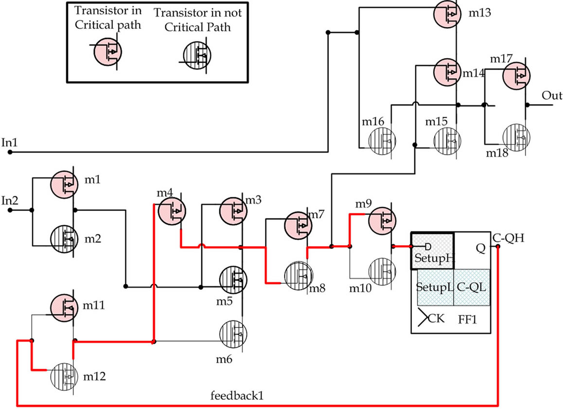
Figure 8. Simple sequential circuit example.
slack times for all transistors in the circuit [24].
The program was tested on several popular circuits with different sizes (inverter, OR, AND, XOR, half adder, full adder, 4 bit, 8 bit, 12 bit carry ripple adder and 4 bit
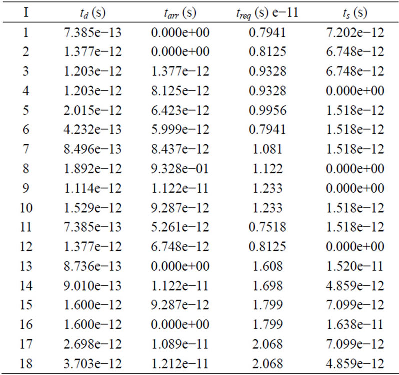
Table 3. Timing parameters for combinational sub-circuit.
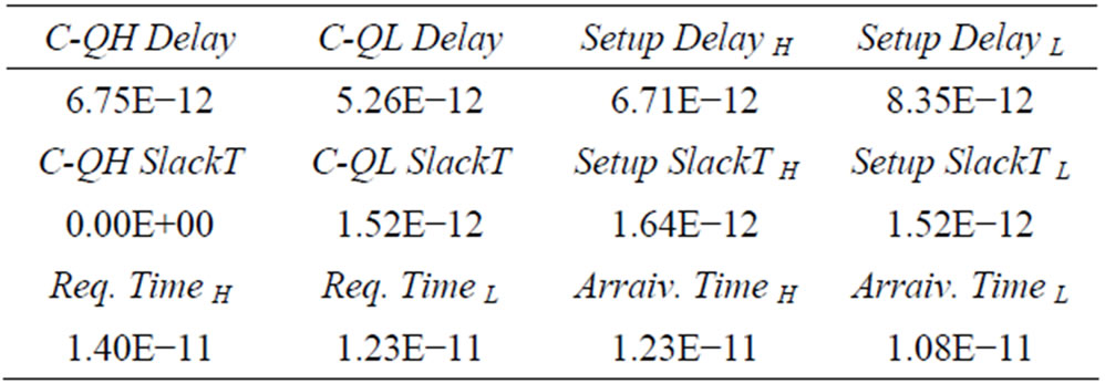
Table 4. Timing parameters in second for sequential subcircuit.
parallel multiplier). The simulation results show that the proposed algorithms are valid for all test cases because it does not get in any dead lock situation and return accurate results. To illustrate the program results a traditional full adder circuit is chosen as a study case.
Full Adder Circuit
The conventional Full Adder of 28 transistors is used as an example; the Full Adder has 3 inputs, and 2 outputs. It is attended to use the minimum length (22 nm) in order to reduce the size of transistor and to increase the speed of transistor, and also to reduce dynamic power dissipation. The transistors’ channel widths are selected carefully for each transistor depending on the position of that transistor in the circuit; to balance between the circuit falling and rising times, this circuit is shown in Figure 8. The load capacitance and timing analysis for each transistor in the circuit is shown in Table 3, where td is the delay time of any transistor, tarr is arrival time, and treq is the required time, ts is the slack time.
From Table 5, the arrival time equals zero for transistors 1, 5, 6, 8, 10, 13, 16, 17, 18, 19, 20 and 26 because these transistors are connected to the circuit’s inputs. Also, the required time equals zero for transistors 11, 12, 27 and 28 because these transistors are connected the circuit’s outputs as illustrated in Figure 8. The transistors 1, 2, 3, 6, 15 and 27 have zero slack time because they are located in the circuit critical paths, these transistors make path from the circuit’s input to the circuit’s output.
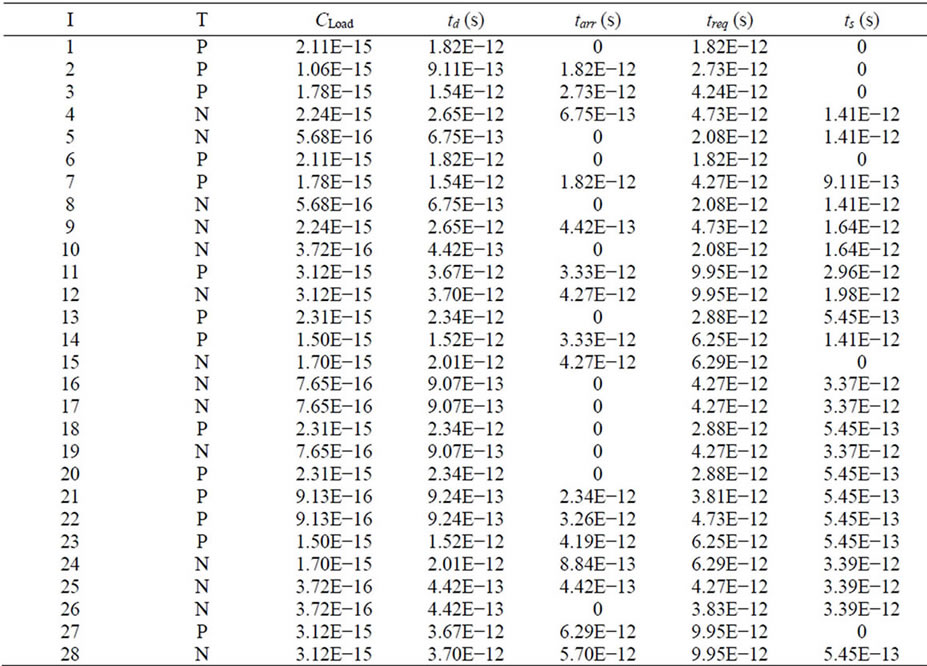
Table 5. Transistors timing analysis in the full adder circuit.
The purpose of this Graph model and algorithms which is built inside a tool is to find the critical path of any CMOS circuit and to calculate slack time in order to optimize the design. Powerful of this model is its capability to show the effects of changing parameter of the transistors located in the non-critical path like size to optimize the silicon area, or transistor Vth to optimize leakage power dissipation. During this optimization process the circuit delay slack times recalculated for every transistor after every change in the circuit in order to find the optimal design. To illustrate that greedy search algorithm is applied on the case study circuit in order to optimize leakage power dissipation. In each iterate during the search, Vth of one transistor that located in non-critical path is change to high and the delay and slack times are recalculated to all transistors. Figure 10 shows and example of one-bit conventional Full Adder of 24 transistors before the optimization using the proposed technique, while Figure 11 shows the same design after the optimization process where the leakage power is reduced 45% which is the optimal result by using to value of Vth.
The same optimization process was applied on several popular circuits with different sizes (inverter, OR, AND, XOR, full adder, 4 bit, 8 bit, 12 bit carry ripple adder and 4 bit parallel multiplier) Table 6 show results of power reduction and number of iteration that required for optimization in these circuits by using PC with Intel CPU at 3.00 GHz frequency.
The simulation results from Table 6 show that the proposed algorithms are valid for all test cases because it does not get in any dead lock situation and work effectively during the optimization process. Although the number of iterations increased exponentially with increasing number of the circuits’ transistors, the time required for optimization is acceptable and extremely fast compared to the traditional models for timing at transistor level.

Figure 10. Conventional 28_transistor full adder circuit.
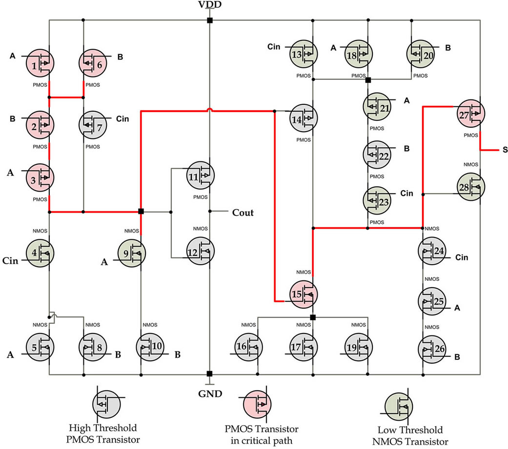
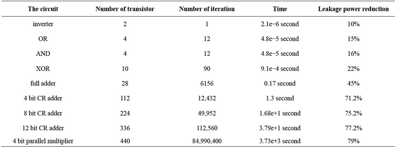
Table 6. Leakage power reduction and in tested circuits.
5. Conclusion
In this paper, the methodology and algorithm used for delivering Static Timing Analysis for CMOS circuit at transistor level based on the transformed graph are shown; these were applied to solve timing problems with the exploitation of time for area and power optimization. This new methodology is based on accurate timing equations for nanometer CMOS transistors and more fast and accurate when compared to the traditional models for timing, we have introduced the principles of timing analysis resulting with the slack component. It has been shown in this paper that slack time provides a very important metric which give an opportunity to optimize circuit area and power performances. In terms of timing arrival, required slack times are found for every transistor, thus setup, Clock to Q timings are found for every sequential element. The simulation results show that the proposed algorithms are valid for all test cases because it does not get in any dead lock situation and work effectively during the optimization process.
REFERENCES
- K. Bard, B. Dewey, M.-T. Hsu, T. Mitchell, K. Moody, V. Rao, R. Rose, J. Soreff and S. Washburn, “TransistorLevel Tools for High-End Processor Custom Circuit Design at IBM,” IEEE Proceedings of the Journal, Vol. 95, No. 3, 2007, pp. 530-554. doi:10.1109/JPROC.2006.889385
- Z. T. Li and S. M. Chen, “Transistor Level Timing Analysis Considering Multiple Inputs Simultaneous Switching,” IEEE Proceedings of 10th Computer-Aided Design and Computer Graphics, Beijing, October 2007, pp. 315-320.
- C. H. Chen, X. J. Yang and M. Sarrafzadeh, “Potential Slack: An Effective Metric of Combinational Circuit Performance,” IEEE International Conference on ComputerAided Design, San Jose, 5-9 November 2000, pp. 198-201.
- M. Naresh and S. Sachin, “Timing Analysis and Optimization of Sequential Circuits,” Kluwer Acadimic Publisher Group, 1999.
- F. Sill and F. G. D. Timmermann, “Total Leakage Power Optimization with Improved Mixed Gates,” Proceedings of the 18th Symposium on Integrated Circuits and System Design, Florianolpolis, 4-7 September 2005, pp. 154-159.
- R. Nair, C. L. Berman, P. S. Hauge and E. J. Yoffa, “Generation of Performance Constraints for Layout,” IEEE Transactions on Computer-Aided Design, Vol. 8, No. 8, 1989, pp. 860-874. doi:10.1109/43.31546
- T. Gao, P. M. Vaidya and C. L. Liu, “A New Performance Driven Placement Algorithm,” Proceedings of IEEE International Conference on Computer Aided Design, Santa Clara, 11-14 November 1991, pp. 44-47.
- H. Youssef and E. Shragowitz, “Timing Constraints for Correct Performance,” IEEE Proceedings of International Conference on Computer Aided Design, Santa Clara, 11-15 November 1990, pp. 24-27.
- S. Dutta, S. Nag and K. Roy, “ASAP: A Transistor Sizing Tool for Speed, Area, and Power Optimization of Static CMOS Circuits,” International Symposium of Circuits and Systems, London, 30 May-2 June 1994, pp. 61-64.
- H.-Y. Song, K. Nepal, R. I. Bahar and J. Grodstein “Timing Analysis for Full-Custom Circuits Using Symbolic DC Formulations,” IEEE Transactions on Computer-Aided Design Integral Circuits Systems, Vol. 25, No. 9, 2006, pp. 1815-1830.
- K. S. Hedlund, “Aesop: A Tool for Automated Transistor Sizing,” Proceedings of the 24th ACM/IEEE conference on Design automation, Miami Beach, 28 June-1 July 1987, pp. 114-120.
- U. Seckin and C.-K. K. Yang, “A Comprehensive Delay Model for CMOS CML Circuits,” IEEE Transactions on Circuits and Systems I, Vol. 55, No. 9, 2008, pp. 2608-2618. doi:10.1109/TCSI.2008.920069
- B. Rich.man, J. Hansen and K. Cameron, “A Deterministic Algorithm for Automatic CMOS Transistor Sizing,” IEEE Proceedings of Conference on Custom Integmted Circuits Conference, Portland, 4-7 May 1987, pp. 421-424.
- S. Raja, F. Varadi, M. Becer and J. Geada, “Transistor Level Gate Modeling for Accurate and Fast Timing, Noise, and Power Analysis,” Proceedings of Design Automation Conference, Anaheim, 8-13 June 2008.
- R. Rogenmoser and Kaeslin, “The Impact of Transistor Sizing on Power Efficiency in Submicron CMOS Circuits,” IEEE Journal of Solid-State Circuits and systems, Vol. 32, No. 7, 1997, pp. 1142-1145.
- W. Yang and M. Dunga, Eds., “BSIM4.6.1 MOSFET Model, User Manual,” 2008. http://www.devices.eecs.berkely.edy/~bsim3/bsim4.html
- D. Blaauw, K. Chopra, A. Srivastava and L. Scheffer, “Statistical Timing Analysis: From Basic Principles to State of the Art,” IEEE Transactions on Computer-Aided Design of Integrated Circuits and Systems, Vol. 27, No. 4, 2008, pp. 589-607. doi:10.1109/TCAD.2007.907047
- A. Jain and D. Blaauw, “Slack Borrowing in Flip-Flop Based Sequential Circuits,” Proceedings of the 15th ACM/ IEEE Great Lakes Symposium on VLSI, Chicago, 17-19 April 2005, pp. 96-101.
- A. Dendouga, N. Bouguechal, S. Barra and O. Manck, “Timing Characterization and Layout of a Low Power Differential C2MOS Flip-Flop in 0.35 μm Technology,” 2nd International Conference on Electrical Engineering Design and Technologies, Hammamet, 8-10 November 2008, pp. 1-4.
- P. Y. Calland, A. Mignotte, O. Peyran, Y. Robert and F. Vivien, “Retiming DAG’s (Direct Acyclic Graph),” IEEE Transaction on Computer-Aided Design Integrated Circuits and Systems, Vol. 17, No. 12, 1998, pp. 1319-1325. doi:10.1109/43.736571
- K. Choi and A. Chatterjee, “PA-ZSA (Power Aware Zero Slack Algorithm): A Graph Based Timing Analysis for Ultra Low-Power CMOS VLSI,” Proceedings of the Power and Timing Modeling, Optimization and Simulation, Seville, 11-13 September 2002, pp. 178-187.
- C.-P. R. Liu and J. A. Abraham, “Transistor Level Synthesis for Static CMOS Combinational Circuits,” Ninth Great Lakes Symposium on VLSI, Austin, 4-6 March 1999, pp. 172-175,
- Nanoscale Integration and Modeling (NIMO) Group, Predictive Technology Model (PTM), 2008. http://www.eas.asu.edu/~ptm/
- A. Rjoub and A. B. Alajlouni, “Graph Modeling for Static Timing Analysis at Transistor Level in Nano-Scale CMOS Circuits,” IEEE Proceedings of the 16th Mediterranean Electrotechnical, Yasmine Hammamet, 25-28 March 2012, pp. 80-83.
NOTES
*This paper is an extended version of Graph modeling for Static Timing Analysis at transistor level in nano-scale CMOS circuits, published in MELECON12, pp. 80-83, date March 2012, ISSN 2158-8473.
#Corresponding author.