Journal of Modern Physics
Vol.2 No.12(2011), Article ID:16500,7 pages DOI:10.4236/jmp.2011.212176
Investigation of Negative Refraction Phenomenon for Au Nanowires Array Tuning with Index of Filling Material
1School of Physical Electronics, University of Electronic Science and Technology of China, Chengdu, China
2State Key Laboratory of Applied Optics, Changchun Institute of Optics, Fine Mechanics and Physics, Chinese Academy of Sciences, Changchun, China
3Opto-Electronic Technology Center, Changchun Institute of Optics, Fine Mechanics and Physics, Chinese Academy of Sciences, Changchun, China
E-mail: yqfu@uestc.edu.cn, yuwx@icomp.ac.cn
Received September 16, 2011; revised October 22, 2011; accepted November 10, 2011
Keywords: Au Nanowires array, Negative refractive index, FDTD, radius, index of filling material
ABSTRACT
Negative refraction performance of Au nanowires arrays-based metamaterials was explored by means of finite difference and time domain (FDTD) algorithm for the purpose of providing flexible design freedom of the negative index metamaterials (NIMs) working in visible regime from nanofabrication point of view. Tuning performance of the nanowires for negative refraction was analyzed by use of varying refractive index of filling materials among the metallic nanowires. Computational numerical simulation and analyses were carried out. The performance of negative refraction was compared by optimization of the structures. By optimizing the nanowires radius, E-field intensity was calculated in the case that the refractive index of filling material is changeable. The calculated refraction angles illustrate a relationship between the refraction angle and the index of filling material. Our computational results demonstrate that effective value of the negative refractive index strongly depends on the refractive index of the filling material when other parameters are fixed.
1. Introduction
Sub-diffraction imaging has attracted numerous interests in the scientific community, and in recent years there has been much interest in the propagation of electromagnetic waves in artificial materials, particularly in the materials with a negative index of refraction [1-4]. Negative refraction is a fantastical phenomenon that is demonstrated interaction between light and matter. The corresponding negative refraction materials have become hot spot for researchers in many areas such as physics, materials science, and electronic science. Negative refraction materials are special materials that dielectric constant e and magnetic permeability m are simultaneously negative, and refractive index is less than zero, which are also known as ‘left-hand’ materials or both negative materials. Therefore, the negative refractive index materials are appealing for researchers in comparison to conventional materials. It prompts the booming research in nano-optics and nanophotonics. Many physical phenomena such as beyond diffraction limit and the tentative idea of ultrasmall nano-optical devices appear because of many interesting physical phenomena on surface plasmon polaritons (SPPs). A typical example is artificial nanostructure-based negative refraction. The idea of negative refraction appeared quite early. Negative refraction and backward propagation of waves were described by Mandelshtam, and which was published in his textbook in 1944 [5]. He described backward-wave transmission lines in 1951 [6]. Then Russian scientist Veselago presented the phenomenon of negative refraction theoretically in 1968 [1]. He demonstrated the phenomenon in metamaterialsbased structures and photonic band gap materials [7-9]. British scientist Pendry proposed a flat refractive index is –1 in 1998 [10], which can be used as a lens material to achieve a perfect imaging and can magnify the potential evanescent wave making the size of image breaking the optical diffraction limit. Eleftheriades described planar “left handed” isotropic media with perpendicular polarization of electric field firstly [11]. A double interface transmission line lens was theoretically described in [12] and its design and testing results were presented in 2005 [13]. Smith synthesized negative refractive material firstly in 2000 [14], and demonstrated an artificial negative refractive material through experiments. After that, a Snell’s law experiment was performed on a wedgeshaped metamaterial which was designed to have a negative refractive index at microwave frequencies in 2001 [15]. However, the main problem with all of the early works was that these ideas remained only a scientific curiosity due to the technological limitation. Nevertheless, with mature of microfabrication and nanofabrication, new possibilities opened for practical implementation of different metamaterials. And the field became intensely studied by many research teams. A first negative index metamaterials (NIMs) working in visible regime was reported by Zhang et al. in 2008 [16]. It was fabricated using porous alumina template approach. However, structural parameters of the Ag/Al2O3-based nanowires are fixed due to the inherent diameter of the porous alumina template naturally formed by means of wet chemical etching. It means that the structure cannot be designed theoretically in advance. In other words, there is no design freedom for their reported Ag nanowires structures. Reference [17] assessed the possibility of near-field subwavelength imaging at infrared frequencies using an array of thin silver rods. And in Ref. [18], the authors proposed a nonlocal permittivity model to describe the electrodynamics of plasmonic rods.
In Reference [19], Kawata et al. demonstrated the possibility of using metallic nanorods to achieve sub-diffraction resolution in the optical domain on the basis of excitation and propagation of surface plasmon polartions (SPPs). Fortunately, current nanofabrication techniques such as e-beam writing and focused ion beam direct milling (FIBM) can be used to produce the regular and size controllable structures which may be used as NIMs. Considering this, we studied characteristics of Au nanowires array-based NIMs with tunable geometrical parameters which have good manufacturability for e-beam or FIBM for the purpose of providing flexible design freedom of the NIMs working in visible regime. In practice, the metallic nanowires array cannot be suspended in air. A filling material among the wires is requisite in real applications. On the other hand, in nanofabrication point of view, filling material of the nanowires array is also a crucial issue to influence the nanowires on both manufacturability and performance of negative refraction. Considering this, we carried out the study of influence of tuning filling material index on performance of negative refraction. The nanowires array is formed by ideally conducting wires with a regular lattice and small radii compared to the lattice periods and the wavelength.
In this paper, we investigated characteristics of the Au nanowires arrays which can realize negative refraction, and its refractive index changes with variation of the filling material. In order to obtain the trend of refraction angle vs the index of filling material, the electric field intensity distribution at the same location of the image plane and the refraction angle were calculated. We analyzed and compared the electric field intensity distribution for different periodic structures. From the analyses results, we concluded that the intensity of the negative refraction using the NIMs when fill material among wires strongly depends on the relationship with the filling material.
2. Numerical Simulation Setup
Schematic diagram of the structure of nanowires array is shown as Figure 1. The thickness of the slab is Z, and the whole medium is air in addition to among the Au nanowires is PC (polycarbonate). We applied Finite difference and time domain (FDTD) algorithm for the theoretical calculation and analyses. FDTD algorithm is a commonly used approach in computational electromagnetic fields. It has extensive applications because of
 (a)
(a)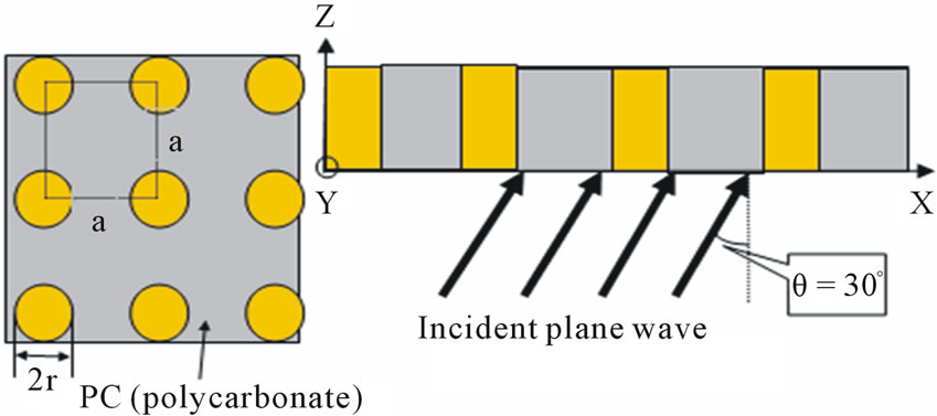 (b)
(b)
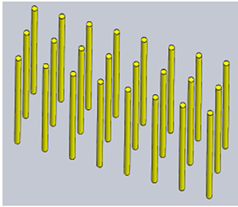
Figure 1. (a) Schematic diagram of nanowires array composed of many metal wires, the material is Au. Among the nanowires is the filling material PC (polycarbonate). (b) wire radius and the index of filling material varies for the periodic structures. The incident angle of plane wave is 30˚, wave area in X direction is 1 mm, and wavelength is 633 nm.
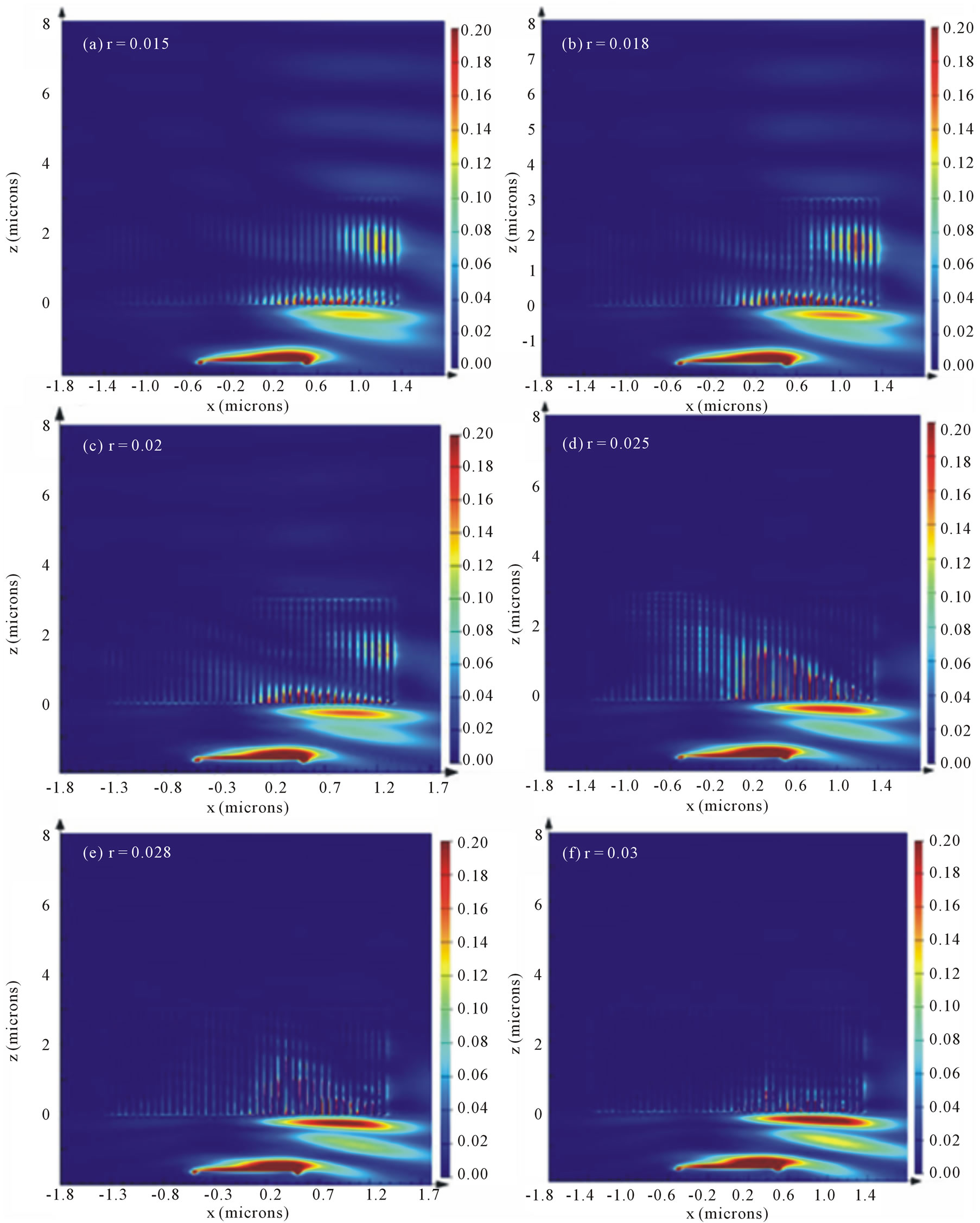
Figure 2. E-field intensity distribution along X-Z plane for periodic structure, incident wave is 633 nm, the index of filling material is 1.05, period a is 0.07 mm , Z = 3 mm radius r is (a) 0.015 mm; (b) 0.018 mm; (c) 0.02 mm; (d) 0.025 mm; (e) 0.028 mm; and (f) 0.03 mm respectively.
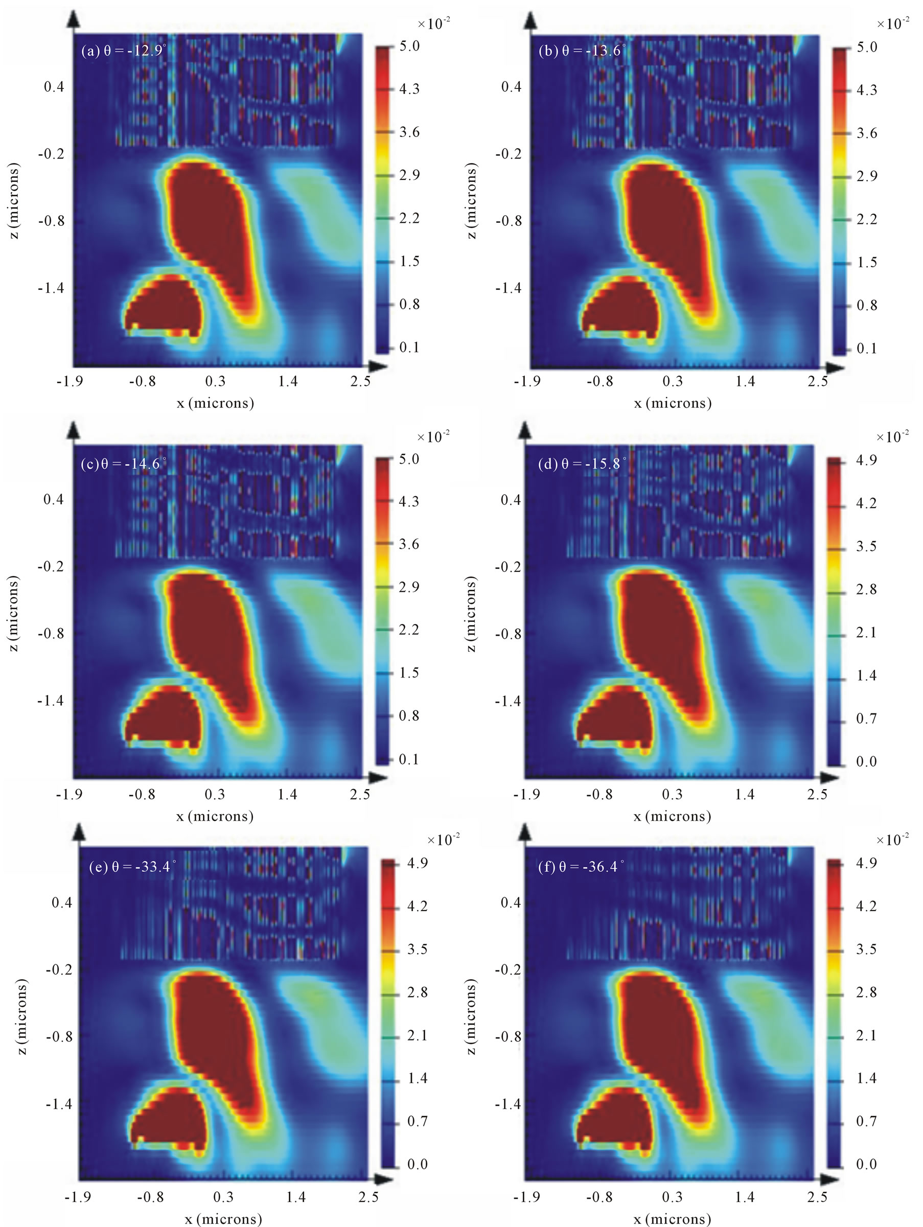
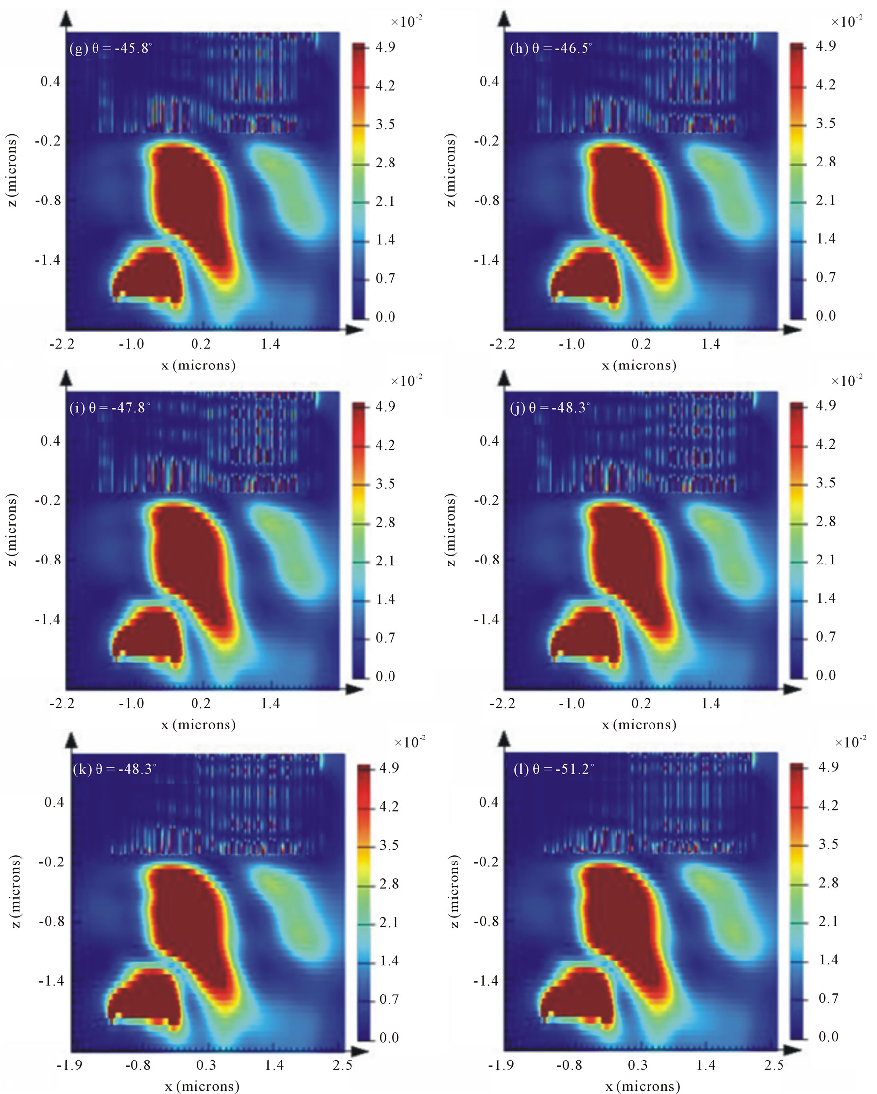
Figure 3. E-field intensity distribution along X-Z plane for periodic structure, incident wave is 633 nm, Z = 1 mm, radius r is 0.025 nm, and period a is 0.07nm, the index of filling material is (a) n = 0; (b) n = 1; (c) n = 1.05; (d) n = 1.1, (e) n = 1.15; (f) n = 1.2; (g) n = 1.25; (h) n = 1.3; (i) n = 1.35; (j) n = 1.4; (k) n = 1.45; (l) n = 1.5 respectively. Every approximate refractive angle is shown also.
its advantages such as easily understanding, direct timedomain calculation, saving memory space and computation time, and broad applicability [20]. Three factors were considered in the calculation: incident wavelength l, wire radius r, the index of filling material n and period a. Material of the nanowires is Au, and incident wavelength is 633 nm. In nanofabrication point of view, radius r used for the calculation is 0.015 mm, 0.018 mm, 0.02 mm, 0.025 mm, and 0.03 mm respectively. Period a is 0.07 mm. Length Z is ranging from 1 mm, 1.5mm and 3 mm. Incident plane wave is linear x-polarization with assumed amplitude of 1 and incident angle of 30˚. In our three-dimensional (3D) simulation, time and mesh size were set as 500 fs, Δx = 6 nm, and Δy = 6 nm respecttively for the periodic structures. Then we simulated the following structures respectively in the sections below.
3. Results and Discussions
We discussed characteristics of negative refraction with the index of filling material changing for the same NIMs structures shown in Figure 1 from the visual map.
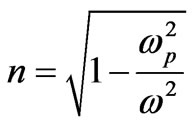
Figure 2 shows the E-field intensity distribution in X-Z plane when r is changeable. Wavelength and position of incident plane wave is 633 nm, and Z = 3 mm, respectively. From the color bar we obtain that transmission intensity is different. It can be seen from the figures that transmission intensity for the case of r = 0.025 mm is stronger than the others. Therefore, we can choose the parameters r = 0.025 mm, a = 0.07 mm as the optimized case. From the above results we can know that choosing Z = 1 mm is better. Figure 3 is calculated intensity vs the index of filling material in the case of r = 0.025 mm, a = 0.07 mm, and Z = 1 mm. As can be seen that the intensity of among nanowires decreases with increasing of index of filling material, but the intensity of beyond nanowires decreases with increasing of the index of filling material when index is below 1.10, when index n is above 1.10 the intensity increases . It can be seen from Table 1 that refraction angle q decreases with index n (the index of filling material) increasing. The negative refraction index increases accordingly. It can be explained using the formula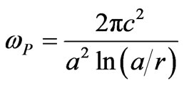 , where c is the light speed in vacuum, and wp is the plasma frequency which decreases with increasing a [21]. Thus we know from equation
 that effective n will increase, and q increases accordingly.
Figures 4 and 5 show the E-field intensity profiles along X-axis. The structure parameter is the same as that of shown in Figure 3. And the wire position is y = 0,
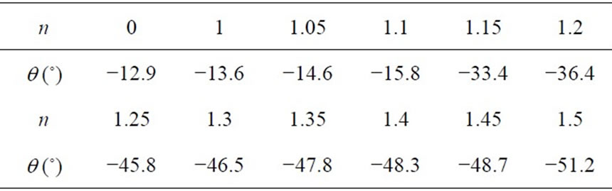
Table 1. Incident angle q = 30˚, refraction angle q vs the index of filling material n for the periodic structures.
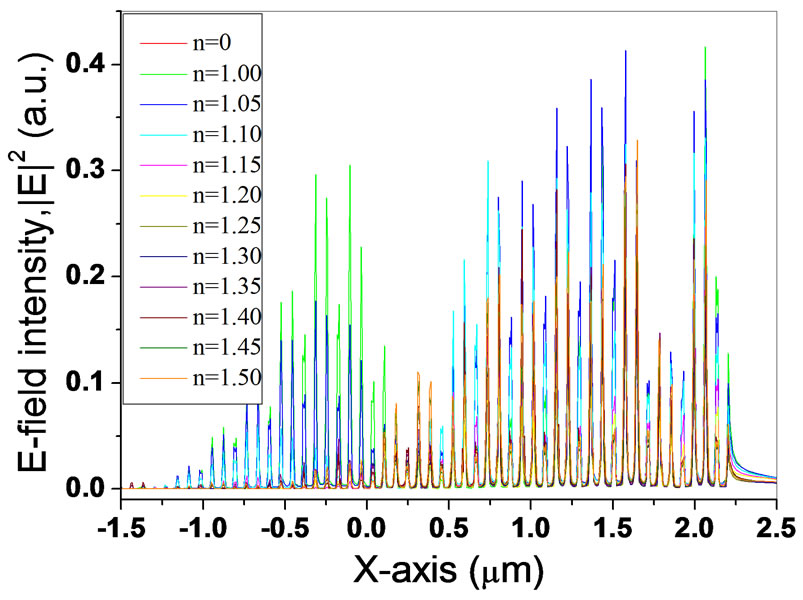
Figure 4. E-field intensity distribution along X axis for periodic structure, incident plane wave is 633 nm, radius r is 0.025nm, and period a is 0.07 nm y = 0, Z = 1 mm, the index of filling material is (a) n = 0; (b) n = 1; (c) n = 1.05; (d) n = 1.1; (f) n = 1.2; (h) n = 1.3; (j) n = 1.4; (k) n = 1.4, and (m) n = 1.5 respectively.
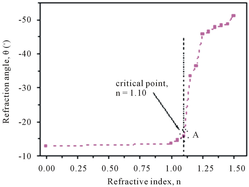
Figure 5. The angle of negative refraction as function of the index of filling material n.
length Z = 1 mm. It can be seen that when the index of filling material changes the intensity and refraction area change also. In the case of n = 1.10 (marked with circle A with dot line in Figure 5), intensity reaches maximum. Namely, the derived effective refractive index n0 is tunable in various n (the index of filling material). It is attractive for both design and nanofabrication issues.
4. Conclusions
We have illustrated the optical properties of Au nanowires array by means of a rigorous computational numerical calculation to analyze the negative refraction and transmission properties in my last paper. The analytical results show that the refraction and transmission properties have close relationship. Both of them depend on the structure parameters when the nanowires width is enough big, there is phenomenon of positive refraction. From the above analysis we can obtain that when the index of filling material n is above 1.10, the transmission intensity of negative refraction and positive refraction decreases with the index increasing.
5. Acknowledgements
The research work was supported by National Natural Science Foundation of China (No. 11079014 and 61077010).
REFERENCES
- V. G. Veselago, “The Electrodynamics of Substances with Simultaneously Negative Values of Epsilon and mu,” Soviet Physics Uspekhi, Vol. 10, No. 4, 1968, pp. 509-514. doi:10.1070/PU1968v010n04ABEH003699
- R. A. Shelby, D. R. Smith and S. Schultz, “Experimental Verification of a Negative Index of Refraction,” Science, Vol. 292, No. 5514, 2001, pp. 77-79. doi:10.1126/science.1058847
- P. A. Belov and C. R. Simovski, “Canalization of Subwavelength Images by Electromagnetic Crystals,” Physical Review B, Vol. 71, No. 19, 2005, pp. 193105-193109. doi:10.1103/PhysRevB.71.193105
- P. A. Belov, Y. Hao and S. Sudhakaran, “Subwavelength Microwave Imaging Suing an Array of Parallel Conducting Wires as a Lens,” Physical Review B, Vol. 73, No. 3, 2006, pp. 033108-033112. doi:10.1103/PhysRevB.73.033108
- L. I. Mandelshtam, “Lectures on Some Problems of the Theory of Oscillations,” Complete Collection of Works, Vol. 5, Academy of Sciences, Moscow, 1944, pp. 428- 467.
- G. D. Malyuzhinets, “A Note on the Radiation Principle,” Soviet Physics—Technical Physics, Vol. 21, 1951, pp. 940-942.
- M. Notomi, “Theory of Light Propagation in Strongly Modulated Photonic Crystals: Refractionlike Behavior in the Vicinity of the Photonic Band Gap,” Physical Review B, Vol. 62, No. 16, 2000, pp. 10696-10705. doi:10.1103/PhysRevB.62.10696
- D. R. Smith, W. Padilla, D. C. Vier, S. C. Nemat-Nasser and S. Schultz, “Composite Medium with Simultaneously Negative Permeability and Permittivity,” Physical Review Letters, Vol. 84, No. 18, 2000, pp. 4184-4187. doi:10.1103/PhysRevLett.84.4184
- C. Luo, S. G. Johnson, J. D. Joannopoulos and J. B. Pendry, “Subwavelength Imaging in Photonic Crystals,” Physical Review B, Vol. 65, No. 20, 2002, pp. 201104- 201108. doi:10.1103/PhysRevB.65.201104
- J. B. Pendry, A. J. Holden, D. J. Robbins and W. J. Stewart,” Low Frequency Plasmons in Thin Line Structures,” Journal of Physics: Condensed Matter, Vol. 10, No. 22, 1998, pp. 4785-4788. doi:10.1088/0953-8984/10/22/007
- G. V. Eleftheriades and A. K. Iyer, “Planar Negative Refractive Index Media Using Periodically L–C Loaded Transmission Lines,” IEEE Transactions on Microwave Theory and Techniques, Vol. 50, No. 12, 2002, pp. 2702- 2712. doi:10.1109/TMTT.2002.805197
- A. Grbic and G. V. Eleftheriades, “Growing Evanescent Waves in Negative-Refractive-Index Transmission-Line Media,” Applied Physics Letters, Vol. 82, No. 12, 2003, pp. 1815-1818. doi:10.1063/1.1561167
- A. Grbic and G. V. Eleftheriades, “Practical Limitations of Subwavelength Resolution Using Negative-Refractive-in-Dex Transmission-Line Lenses,” IEEE Transactions on Antennas and Propagation, Vol. 53, No. 10, 2005, pp. 3201-3209. doi:10.1109/TAP.2005.856316
- D. R. Simth, W. J. Padilla and D. C. Vier, “A Composite Medium with Simultaneously Negative Permeability and Permittivity,” Physical Review Letters, Vol. 84, No. 18, 2000, pp. 4184-4187. doi:10.1103/PhysRevLett.84.4184
- A. M. Belyantsev and A. B. Kozyrev, “Reversed Doppler Effect under Reflection from a Shock Electromagnetic Wave,” Technical Physics, Vol. 47, No. 11, 2002, pp. 1477. doi:10.1134/1.1522123
- J. Yao, Z. W. Liu, Y. M. Liu, Y. Wang, C. Sun, G. Bartal, A. M. Stacy and X. Zhang, “Optical Negative Refraction in Bulk Metamaterials of Nanowires,” Science, Vol. 321, No. 5891, 2008, p. 930. doi:10.1126/science.1157566
- M. G. Silveirinha, P. A. Belov and C. R. Simovski, “Subwavelength Imaging at Infrared Frequencies Using an Array of Metallic Nanorods,” Physical Review B, Vol. 75, No. 3, 2007, pp. 035108-035120. doi:10.1103/PhysRevB.75.035108
- M. G. Silveirinha, “Nonlocal Homogenization Model for a Periodic Array of ε-Negative Rods,” Physical Review E, Vol. 73, No. 4, 2006, pp. 046612-046620. doi:10.1103/PhysRevE.73.046612
- A. Ono, J. I. Kato and S. Kawata, “Subwavelength Optical Imaging through a Metallic Nanorod Array,” Physical Review Letters, Vol. 95, No. 26, 2005, pp. 267407-267411. doi:10.1103/PhysRevLett.95.267407
- FDTD Solution, Professional Commercial Software from Lumerical Solution Inc. http://www.lumerical.com.
- Yongqi Fu Edt. E-book, Subwavelength Optics: Theory and Technology. Published by Bentham Sciences, in 2009 in USE, Chapter 12. See website URL below: http://www.benthamscience.com/ebooks/9781608050505/index.htm