Wireless Engineering and Technology
Vol.1 No.2(2010), Article ID:3025,8 pages DOI:10.4236/wet.2010.12008
Performance of Double-Pole Four-Throw Double-Gate RF CMOS Switch in 45-nm Technology
![]()
1Electronics and Communication Engineering Department, Jaypee University of Information Technology, Solan, India; 2VLSI
Design Group, Central Electronics Engineering Research Institute (CEERI), Pilani, India.
Email: viranjay@ieee.org
Received September 7th, 2010; revised September 13th, 2010; accepted September 19th, 2010.
Keywords: 45-nm Technology, Capacitance of Double-Gate MOSFET, DG MOSFET, DP4T Switch, Radio Frequency, RF Switch, Resistance of Double-Gate MOSFET, VLSI
ABSTRACT
In this paper, we have investigated the design parameters of RF CMOS switch, which will be used for the wireless telecommunication systems. A double-pole four-throw double-gate radio-frequency complementary-metal-oxide-semiconductor (DP4T DG RF CMOS) switch for operating at the 1 GHz is implemented with 45-nm CMOS process technology. This proposed RF switch is capable to select the data streams from the two antennas for both the transmitting and receiving processes. For the development of this DP4T DG RF CMOS switch we have explored the basic concept of the proposed switch circuit elements required for the radio frequency systems such as drain current, threshold voltage, resonant frequency, return loss, transmission loss, VSWR, resistances, capacitances, and switching speed.
1. Introduction
In the radio transceiver the switches, traditional n-MOS switch has better performance compare to PIN diodes (use of PIN diodes consumes more power), but only for a single operating frequency [1,2]. For multiple operating frequencies, high signal distortions are easily observed, which results in an unrecognizable information signal at the receiver end which would be measured by using the curve of capacitance and voltage with VEE Pro software [3,4]. A continuous scaling of CMOS technology has a better performance of both frequency and noise, where it is becoming a rigorous part for RF applications in the GHz frequency regime of the spectrum. The aggressive scaling of metal-oxide-semiconductor field effect transistors (MOSFET) has led to the fabrication of high performance MOSFETs with a cut-off frequency (fT) of more than 150 GHz [5]. As a result of this development, the CMOS is a strong candidate for the RF wireless communications in this frequency regime of the specrum.
For the Multiple-Input, Multiple Output systems, it is essential to design a new RF switch that is capable of operating with multiple antennas and frequencies as well as minimizing signal distortion and power consumption [6-8]. The excellent improvement in the frequency response of Si-CMOS devices has aggravated their use in the millimeter-wave regime such as high capacity wireless local area network, short range high data rate wireless personal area networks, and collision avoidance radar for automobiles. Using Si-CMOS for these applications allows for higher levels of integration and lower cost with improving the efficiency. Since for 65-nm technology has application of 60 GHz power amplifier designs [9,10], but recently few research group has demonstrated 60 GHz power amplifiers in 45-nm technologies.
For radio-frequency applications, generally, the common drive requirements for off-chip loads are of 50 Ω impedances. This impedance is a good compromise between lowest loss and highest power handling for a given cable size. Also this impedance caught on for RF transmission sooner than the well established 75 Ω that had been used for video transmission. The nodal capacitance, drain and source sidewall capacitances are the factors which controls the bandwidth of RF switches [11,12]. Since these switches are to be used with digital and baseband analog systems, control by on-chip digital and analog signals is another factor in the design [13].
In the design of DP4T DG RF CMOS switch structures with 45-nm technology for digital and analog, a transaction between speed and frequency response and circuit complexity is always encountered. The properties for RF CMOS switch design for the application in communication and designed results are presented and have been designed to optimize for the particular application [14]. A DP4T DG RF CMOS switch has the properties as fixed tuned matching networks, low quality factor matching networks, high power output, mounting flange packages, and silicon grease. Some bipolar RF CMOS transistors are suitable for automotive, commercial or general industrial applications.
In this paper, we present a comprehensive study of the RF switch performance of 45-nm low-power, high-speed double-pole four-throw double-gate radio-frequency complementary-metal-oxide-semiconductor (DP4T DG RF CMOS) switch. The DP4T DG RF CMOS switch structures with different aspect ratios for 45-nm technology and their layouts are studied to understand the effect of device geometry on working of switching properties. In this design transistor width increases for double-gate MOSFET such that peak power-added efficiency (PAE) and output power Pout decrease as these parameters decreases with increasing device width because of a reduction in fmax [15]. In a RF power amplifier, PAE is defined as the ratio of the difference of the output and input signal power to the DC power consumed. The RF power performance of 45-nm devices is shown to be very comparable to that of 65-nm devices.
An application for a CMOS switch covers the areas of micro power circuits and other wireless applications at frequencies from as low as 0.1 GHz for low earth orbiting satellite system to thousand of GHz [16]. Various circuit parameters have been discussed in this paper for better performance.
Each of the parameters will be discussed separately for the purpose of clarity of presentation and understanding the operation of DP4T DG RF CMOS switch structures for 45-nm technology. The organization of the paper is as follows; DP4T DG RF CMOS switch model is presented in Section 2, Characteristics of DP4T DG RF CMOS switch for layout are discussed in Section 3. The capacitances, Inductances and other parameters present in DG MOSFET for high speed RF switches are discussed in Section 4. The effective resistance of DP4T DG RF CMOS present in switch is discussed in Section 5. Finally, conclusion of the work is in Section 6.
2. DP4T DG RF CMOS Switch Model
The selections of RF CMOS switch require an analysis of performance specifications. Since drain-source breakdown voltage is the maximum drain-source voltage before breakdown with the gate grounded [17], also specifications for RF CMOS transistors includes the maxi-
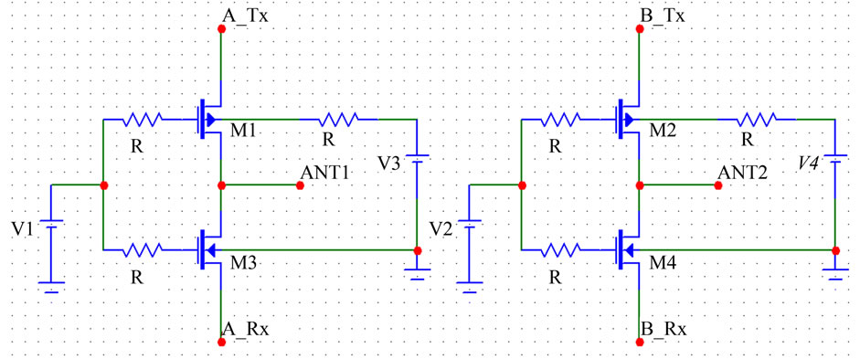
Figure 1. DP4T RF CMOS switch with inverter property [14].
mum drain saturation, common-source forward transconductance, operating frequency, and output power. Devices that operate in depletion mode can increase or decrease their channels by an appropriate gate voltage. By distinction, devices that operate in enhancement mode can only increase their channels by an appropriate gate voltage. RF MOSFET transistors vary in terms of operating mode, packaging, and packing methods.
This paper proposes a design of DP4T DG RF CMOS switch structures at 45-nm technology for low power consumption and low distortion application of RF switch in communication that operates at 0.1 GHz to 60 GHz. The n-channel devices were used in the HF portion of the circuits with p-channel devices used as current sources. The switches which were designed to drive 50 Ω resistive loads and utilized multiple gate fingers to reduce parasitic capacitance is in an effort to improve the operating frequency [13].
The objective of proposed design of a switch is to operate at 0.1 GHz to few GHz frequency range for MIMO systems. This switch must mitigate attenuation of passing signals and exhibit high isolation to avoid corruption of simultaneously received signals [14]. According to the previous work, DP4T switch is a fundamental switch for MIMO applications because parallel data streams can be transmitted or received simultaneously using the multiple antennas. For instance, the transmitted signal from Power Amplifier (PA) is sent transmitter ‘A’ which is shown in Figure 1 with named as ‘A_Tx’ port and travel to the ANT1 node while the received signal will travel from the ANT2 node to the receiver ‘B’ with a named as ‘B_Rx’ port and pass onto the Low Noise Amplifier or any other application.
The proposed switch contains CMOS in its architecture and needs only two control lines (V1, V2) of 1.2 V to control the signal traffic between two antennas and four ports as shown in Figure 1, hence, improving port isolation performance two times, compared to the DPDT switch and reducing signal distortion. In addition, signal fading effects can be reduced because sending identical signals through multiple antennas will most likely result in a high quality combined signal at the receiver end. For the design of DP4T DG RF CMOS switch, we design a

Figure 2. Basic double-gate n-MOSFET.
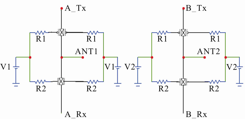
Figure 3. Proposed DP4T DG RF CMOS switch.
double-gate as shown in Figure 2. This shows the double-gate n-MOSFET. Similarly, we can design doublegate p-MOSFET. Now, we convert the Figure 1, DP4T switch using the basic double-gate transistor as shown in Figure 2, for DP4T DG RF CMOS switch as shown in Figure 3.
Since in the Figure 1, four transistors are used for two antennas. In this antenna using the CMOS functionalityat a time any one of transistor M1 or M3 will operate and in the same fashion any one of transistor M2 or M4 will operate. Same function is measured in the proposed DP4T DG RF CMOS switch as in Figure 3. This circuit is designed with a Micro-Cap evaluation 6.0 tool. We can find easily that CMOS based RF switches allow longer battery life than PIN diodes, because current consumption is significantly reduced and also about 60 percent smaller than the smallest GaAs RF switch on the market. Furthermore, our switch also experiences minimal distortion, negligible voltage fluctuation, and low power supply of only 1.2 V. In this switch with compare to Figure 1, for A_Tx and B_Tx, two p-MOS are designed for parallel combination and for A_Rx and B_Rx, two n-MOS are designed for parallel combination which is better selection.
3. Characteristics of DP4T DG RF CMOS Switch for Layout
Figure 4 shows the layout of DP4T DG RF CMOS switch with two input voltages (Vin1 and Vin2) and output through antennas (ANT1 and ANT2) with two transmitters (Tx_A and Tx_B) and two receivers (Rx_A and Rx_B). This layout is drawn with Microwind 3.0 version tool. Here color code has their usual meanings [18,19]. Figure 5 shows the antenna voltages ANT1 and ANT2 with input voltages Vin1 and Vin2 for this transceiver switch. Drain current for this transceiver switch with output voltage is shown in Figure 6, which gives the drain current Idd (max) 0.387 mA, Idd (avg) 0.02 mA, also raise time 36 ps at 1 GHz operating frequency.
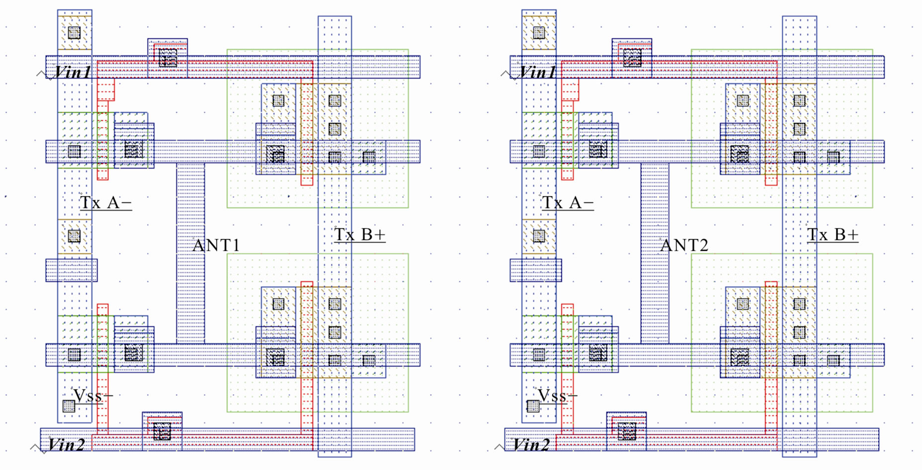
Figure 4. DP4T DG RF CMOS switch layout with antennas.
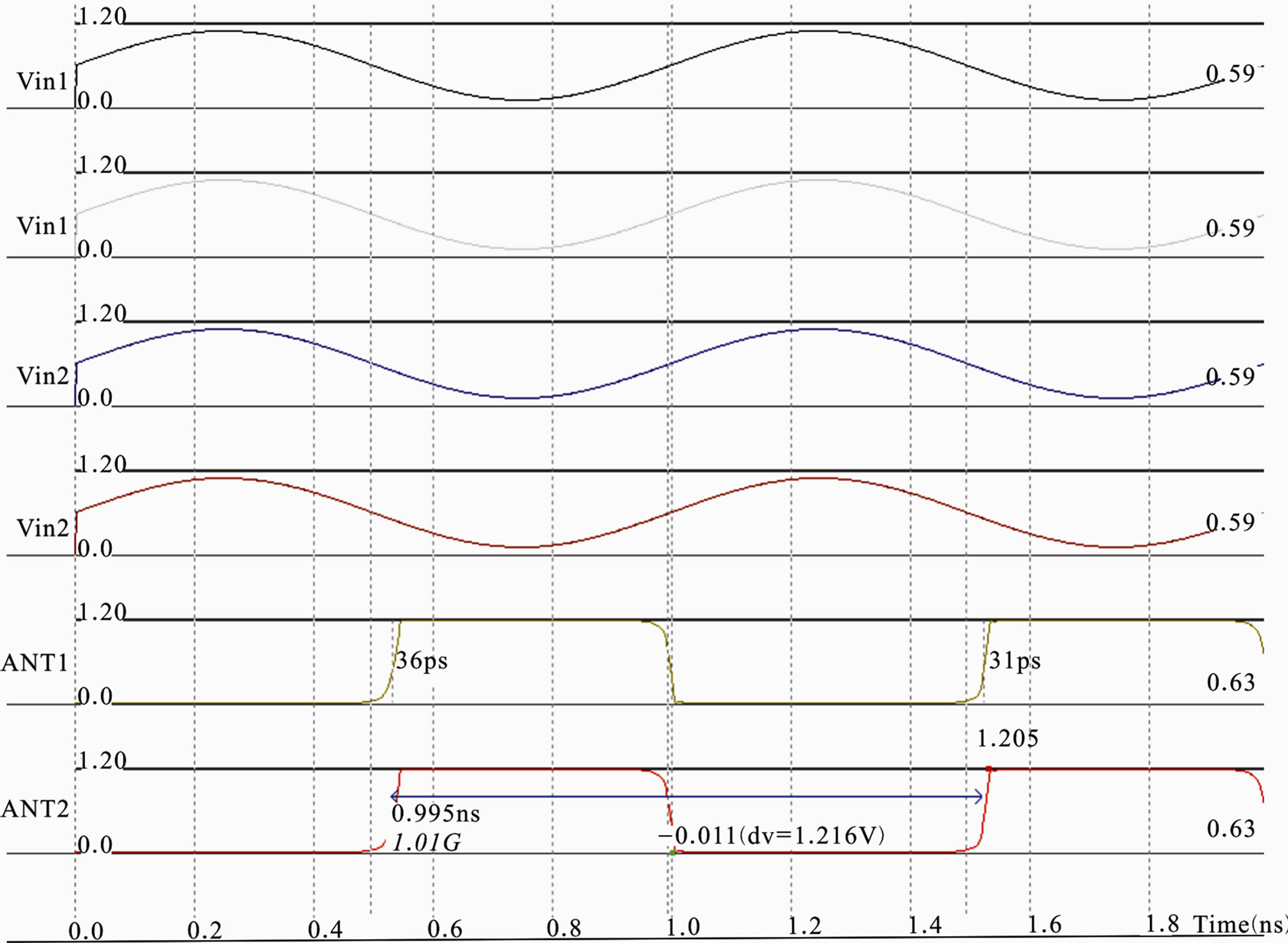
Figure 5. Antenna voltage with input voltages for DP4T DG RF CMOS transceiver switch.
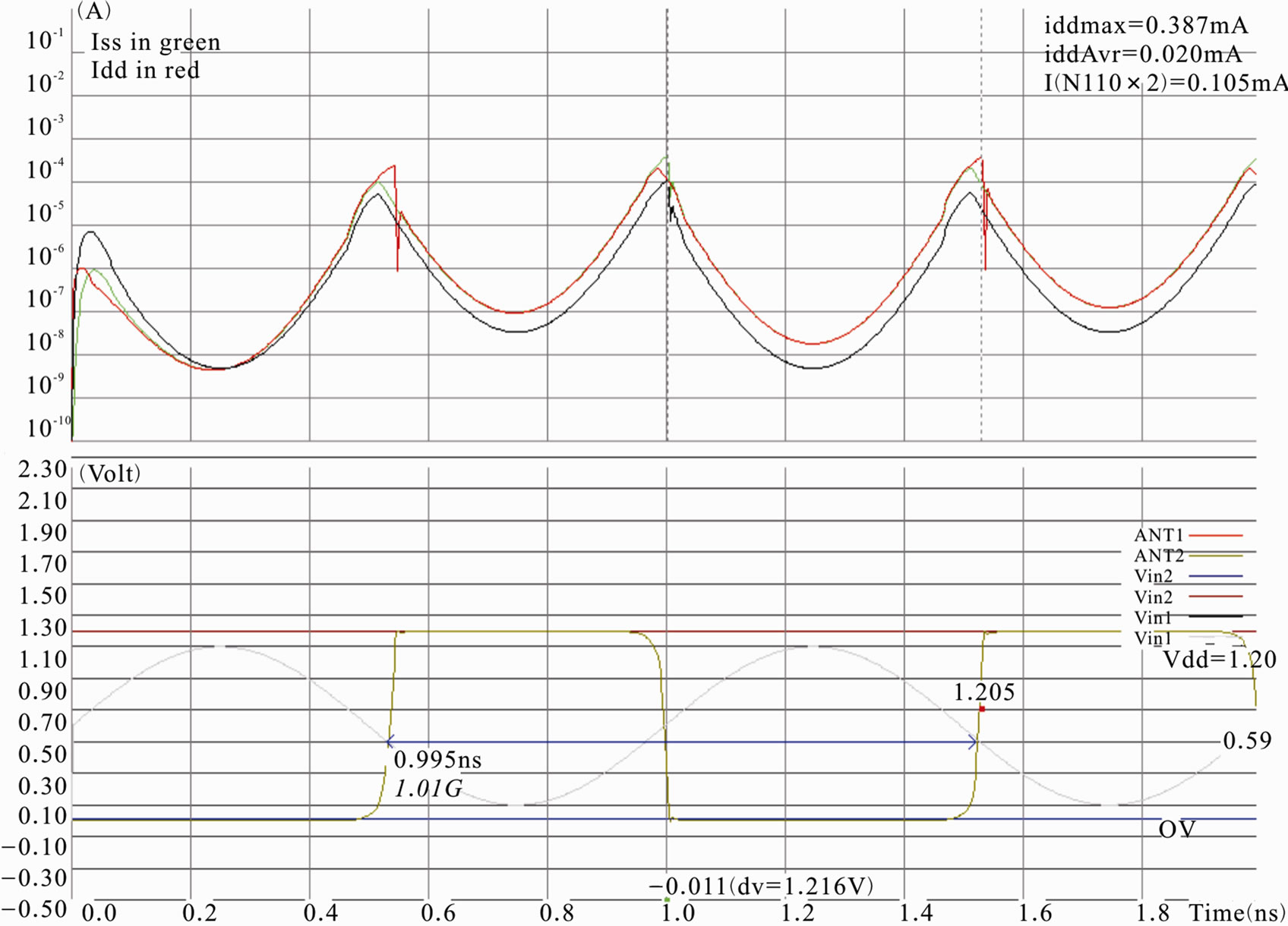
Figure 6. Drain current for DP4T DG RF CMOS transceiver switch with output voltage.
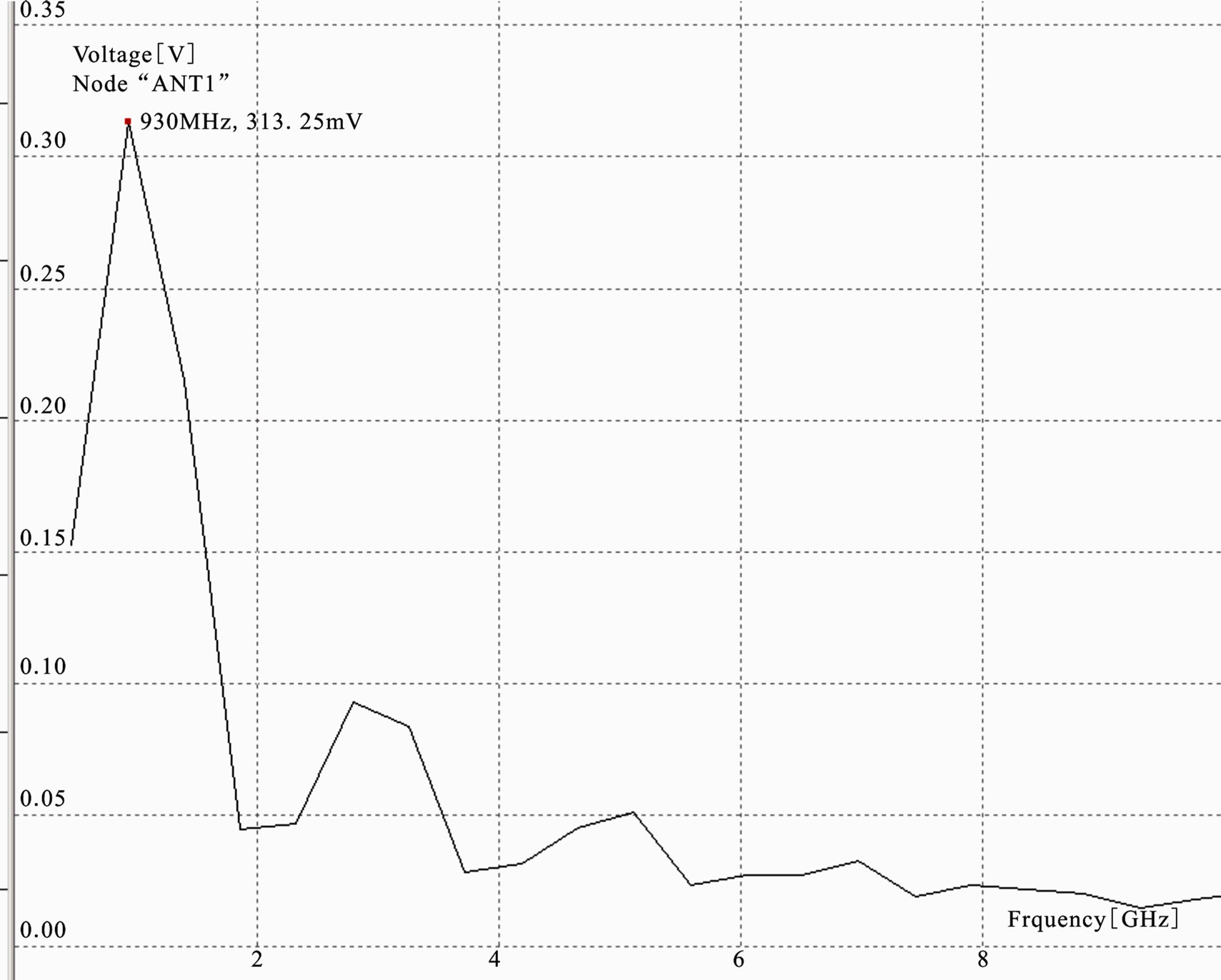
Figure 7. Antenna (ANT1) output with different frequencies for DP4T DG RF CMOS transceiver switch.
In terms of antenna, we draw the first antenna (ANT1) voltage at different frequencies from 0.1 GHz to 8 GHz, in which highest voltage on antenna is achieved at 1 GHz frequency and that is decreases with the increasing frequencies as shown in Figure 7. Also this result is same for second antenna (ANT2).
4. Measurement of Parameters for Double-Gate MOSFET
With the use of Microwind 3.0 version tool for doublegate MOSFET length of 0.045 µm (45 nm) and width of 22.5 µm, we calculate the capacitance of 5.72 fF, inductance of 30 pH, and resistance of 3.12 kΩ. After that we design a DP4T DG RF CMOS switch with help of these values of capacitance, inductance and resistance. A smallsignal performance from few MHz to 100 GHz was measured using RF-99 tool freely available software. Equivalent switch circuit with respect to the capacitance is shown in Figure 8 and the results are shown in Figure 9 and in Table 1.
In detail Figure 9 represents the frequency band, noise power, delay, phase shift, return loss at Tx port, return loss at antenna port, insertion loss measured between Tx port and antenna port, VSWR, transmission loss, reflec tion coefficient. Additional losses associated with cables and connectors, which are quite high at 60 GHz, must be taken into account in the system implementation.
5. Effective Resistance of DP4T RF CMOS Due to Double-Gate
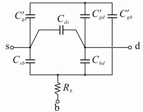
Models of a MOS transistor biased in deep triode region, corresponding to the ON state of the switch, and cut-off region, corresponding to the OFF state of the switch, are shown in Figure 10(a) and Figure 10(b) respectively. The insertion loss of a MOS transistor switch under the ON state is dominated by its ON-resistance (Ron) and substrate resistance (Rb) [20-22]. Isolation of the switch under the OFF state is finite due to signal coupling

Figure 8. Equivalent switch circuit of capacitance.
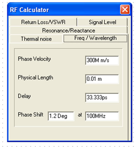
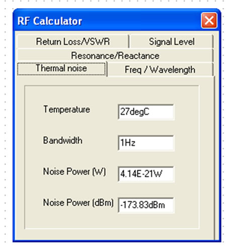
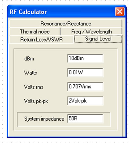
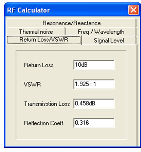
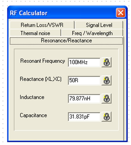
Figure 9. Measurements of parameters for DP4T DG RF CMOS switch.
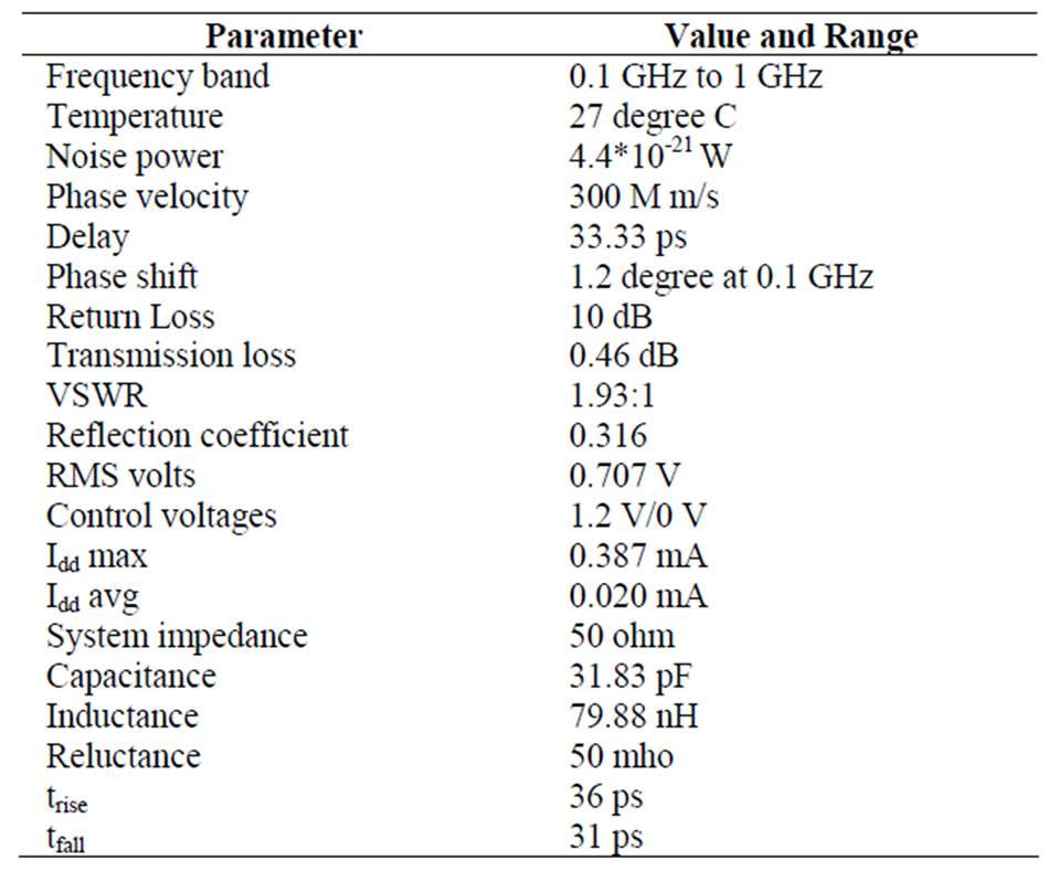
Table 1. Summary of the performance of the double-gate MOSFET T/R switch.
through the parasitic capacitances, Cds, Cgs, and Cgd, and through the junction capacitances, Csb and Cdb.
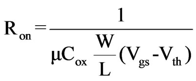
Since the interface contact resistance is inversely proportional to the total gate area as in term of length and width of a gate. The reduction of resistance should lead to improved RF properties in MOSFETs [5,23-28]. In Figure 10 these diodes are represented by their junction capacitances, Csb and Cdb. The ON-resistance is given by;
 (1)
(1)
for proper working of a switch and to reduce the insertion loss, we have to reduce this ON-resistance. So to keep this Ron small, we have to following steps;
5.1. Making Parallel Combination of R
In double-gate switch there are two resistors between drain to source due to gate1 and gate2. Both of these resistors are in parallel so making the Ron half, which keeps Ron small compare to single gate MOS.
5.2. Choosing Transistor with Large μ
This criterion of reducing Ron can be achieved by using n-MOSFET transistors in place of p-MOSFET transistors in the design [22].
5.3. Increasing Aspect Ratio
To increase the ratio of W/L, we have to widening a transistor width (W) and using transistors of minimum allowable channel length (L). Since the minimum value of length is limited by the technology which is 45 nm in this paper that is for transistor length of 0.045 µm and width of 22.5 µm. However, when we increase the width of a transistor, its junction capacitances and parasitic capacitances increases with same ratio. For single gate MOSFET, at ON condition of a transistor, increasing Csb and Cdb tends to more signal being coupled with the substrate and dissipated in the substrate resistance Rb. At OFF condition of the transistor, increasing Cds, Cgd, and Cgs tends to lower isolation between the sources and drain due to capacitive coupling between these terminals
 (a)
(a)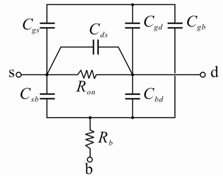 (b)
(b)
Figure 10. Models of a single gate n-MOS transistor operating as a switch in (a) ON state and (b) OFF state [22].
[22]. Whereas for double-gate MOSFET when both the transistors are ON, increasing Csb and Cdb leads to less signal being coupled to the substrate as substrate is not present in this structure, so no dissipation in the substrate resistance Rb. When the transistor is OFF, increasing Cds, Cgd, and Cgs leads to higher isolation between the source and drain due to no capacitive coupling between these terminals.
For low frequency, sufficient isolation can be achieved, so it is not an optimizing parameter for frequencies of order 1 GHz designs. Thus, in these designs, only insertion loss needs to be minimized. No trade-off between insertion loss and isolation is required. On the other hand, at higher frequencies as 60 GHz, isolation is smaller due to several low impedance paths caused by parasitic capacitances. This necessitates a trade-off between insertion loss and isolation during sizing the transistors.
In this designed transistor, width increases for doublegate MOSFET, so peak power-added efficiency and output power decrease as these parameters decreases with increasing device width because of a reduction in fmax [15].
5.4. Keeping Vgs − Vth Large
This criterion can be achieved by increasing the Vgs and decreasing the Vth, so that the difference of these can be large. Threshold voltage has following equation;
 (2)
(2)
where γ is the body effect coefficient and φf is the Fermi level in the substrate. Since in double-gate MOSFET no bulk or substrate is available so γ equals to zero and this decreases the Vth which participate into increasing of the Vgs − Vth . This leads to higher Ron according to (1). In conclusion, by increasing the source-drain voltage, we sacrifice insertion loss for power handling capability.
After designing of DP4T DG RF CMOS switch with designed double-gate MOSFET for 45-nm technology, we draw the layout and measured the parameters available in this switch. It includes the basics of the circuit elements parameter required for the radio frequency sub-systems of the integrated circuits such as drain current, threshold voltage, resonant frequency, return loss, transmission loss, VSWR, resistances, capacitances, and switching speed.
6. Conclusions
For the purpose of RF switch, we achieve the process to minimize control voltage and minimization of the resistance, for the switch ON condition with DP4T DG RF CMOS switch. Since the operating frequencies of the RF switches are in the order of GHz, therefore, it is useful for data link transmitter, radio transceiver switch, wireless local area network and other IEEE 802.11 industrial applications including Wi-Fi system.
REFERENCES
- Skyworks Solutions Inc., “Application Note, APN1002, Design with PIN Diodes,” Woburn, July 2005.
- J. Park and Z. Q. Ma, “A 15 GHz CMOS RF Switch Employing Large Signal Impedance Matching,” Proceeding of Topical Meeting on Silicon Monolithic Integrated Circuits in RF Systems, San Diego, 2006, pp. 1-4.
- V. M. Srivastava, K. S. Yadav and G. Singh, “Application of VEE Pro Software for Measurement of MOS Device Parameter Using C-V Curve,” International Journal of Computer Applications, Vol. 1, No. 7, March 2010, pp. 43-46.
- V. M. Srivastava, “Capacitance-Voltage Measurement for Characterization of a Metal Gate MOS Process,” International Journal of Recent Trends in Engineering, Vol. 1, No. 4, May 2009, pp. 4-7.
- L. E. Microelectron and A. B. Stockholm, “Overlooked Interfacial Silicide-Polysilicon Gate Resistance in MOS Transistors,” IEEE Transactions on Electron Devices, Vol. 48, No. 9, September 2001, pp. 2179-2181.
- J. P. Carmo, P. M. Mendes, C. Couto and J. H. Correia “A 2.4-GHz RF CMOS Transceiver for Wireless Sensor Applications,” Proceeding of International Conference on Electrical Engineering, Coimbra, 2005, pp. 902-905.
- P. Mekanand and D. Eungdamorang, “DP4T CMOS Switch in a Transceiver of MIMO System,” Proceeding of 11th IEEE International Conference of Advanced Communication Technology, Korea, 2009, pp. 472-474.
- P. H. Woerlee, et al, “RF CMOS Performance Trends,” IEEE Transaction on Electron Devices, Vol. 48, No. 8, August 2001, pp. 1776-1782.
- W. L. Chan, et al., “A 60 GHz-Band 1 V, 11.5 dBm Power Amplifier with 11% PAE in 65-nm CMOS,” International Solid State Circuits Conference, San Francisco, 2009, pp. 380-381.
- A. Valdes-Garcia, et al., “60 GHz Transmitter Circuits in 65-nm CMOS,” Radio Frequency Integrated Circuits Symposium, Atlanta, 2008, pp. 641-644.
- Y. Cheng and M. Matloubian, “Frequency Dependent Resistive and Capacitive Components in RF MOSFETs,” IEEE Electron Device Letters, Vol. 22, No. 7, July 2001, pp. 333-335.
- T. H. Lee, “The Design of CMOS Radio-Frequency Integrated Circuits,” 2nd Edition, Cambrige Univrsity Press, New York, 2004.
- R. H. Caverly, S. Smith and J. G. Hu, “RF CMOS Cells for Wireless Applications,” Journal of Analog Integrated Circuits and Signal Processing, Vol. 25, No. 1, 2001, pp. 5-15.
- V. M. Srivastava, K. S. Yadav and G. Singh, “Double Pole Four Throw Switch Design with CMOS Inverter,” Proceeding of 5th IEEE International Conference on Wireless Communication and Sensor Network, 15-19 December 2009, pp. 1-4.
- U. Gogineni, J. Alamo and C. Putnam, “RF Power Potential of 45 nm CMOS Technology,” Proceeding of Topical Meeting on Silicon Monolithic Integrated Circuits in RF Systems, New Orleans, 2010, pp. 204-207.
- T. Manku, “Microwave CMOS Device Physics and Design,” IEEE Journal of Solid State Circuits, Vol. 34, No. 3, March 1999, pp. 277-285.
- S. H. Lee, C. S. Kim and H. K. Yu, “A Small Signal RF Model and Its Parameter Extraction for Substrate Effects in RF MOSFETs,” IEEE Transaction on Electron Devices, Vol. 48, No. 7, July 2001, pp. 1374-1379.
- S. Kang and Y. Leblebici, “CMOS Digital Integrated Circuits Analysis and Design,” 3rd Edition, 2002, McGrawHill, New York, USA.
- R. Baker, H. Li and D. Boyce, “CMOS Circuit Design, Layout, and Simulation,” 3rd Edition, IEEE Press Series on Microelectronic Systems, 2010.
- U. Gogineni, et al., “Effect of Substrate Contact Shape and Placement on RF Characteristics of 45-nm Low-Power CMOS Devices,” IEEE Radio Frequency Integrated Circuits Symposium, Massachusetts, 2009, pp. 163-166.
- F. J. Huang, “A 0.5-μm CMOS T/R Switch For 900 MHz Wireless Applications,” IEEE Journal of Solid-State Circuits, Vol. 36, No. 3, 2001, pp. 486-492.
- C. Ta, E. Skafidas and R. Evans, “A 60-GHz CMOS Transmit/Receive Switch,” IEEE Radio Frequency Integrated Circuits Symposium, Hawaii, 2007, pp. 725-728.
- V. M. Srivastava, K. S. Yadav and G. Singh, “Measurement of Oxide Thickness for MOS Devices, Using Simulation of SUPREM Simulator,” International Journal of Computer Applications, Vol. 1, No. 6, March 2010, pp. 66-70.
- Y. Cheng and M. Matloubian, “Parameter Extraction of Accurate and Scalable Substrate Resistance Components in RF MOSFETs,” IEEE Electron Device Letters, Vol. 23, No. 4, April 2002, pp. 221-223.
- V. M. Srivastava, “Relevance of VEE Programming for Measurement of MOS Device Parameters,” Proceedings of IEEE International Advance Computing Conference, Patiala, March 2009, pp. 205-209.
- S. M. Sze, “Semiconductor Devices: Physics and Technology,” 2nd Edition, Tata McGraw Hill, New Delhi, 2004.
- V. M. Srivastava, K. S. Yadav and G. Singh, “Designing Parameters for RF CMOS Cells,” International Journal of Circuits and Systems, Vol. 1, No. 2, October 2010.
- V. M. Srivastava, K. S. Yadav and G. Singh, “Analysis of Attenuation, Isolation and Switching Speed of DP4T Double Gate RF CMOS Switch Design,” Proceeding of IEEE International Conference on Industrial Electronics, Control & Robotics, NIT Rourkela, 27-29 December 2010.

