Wireless Engineering and Technology
Vol.2 No.1(2011), Article ID:3788,8 pages DOI:10.4236/wet.2011.21001
Optimization of Impedance Plane Reducing Coupling between Antennas
![]()
1Center for Computational Nanosciences, Department of Physics and Astronomy, Ball State University, Muncie, USA; 2Department of Electrical Engineering Advanced Teachers’ Training College for Technical Education, University of Douala, Douala, Cameroon; 3Department of Electrical Engineering and Computer Science, University Institute of Technology, University of Douala, Douala, Cameroon; 4Industrial Engineering Faculty, University of Douala, Douala, Cameroon.
Email: ysjoe@bsu.edu
Received September 2nd, 2010; revised November 5th, 2010; accepted November 19th, 2010.
Keywords: Coupling, Design Optimization, Pointwise Synthesis
ABSTRACT
This paper provides a solution for the design optimization of two-dimensional impedance structures for a given electromagnetic field distribution. These structures must provide electromagnetic compatibility between antennas located on a plane. The optimization problem is solved for a given attenuation of the complete field. Since the design optimization gives a complex law of impedance distribution with a large real part, we employ the method of pointwise synthesis for the optimization of the structure. We also consider the design optimization case where the structure has zero impedance on its leading and trailing edges. The method of moments is used to solve the integral equations and the numerical solution is presented. The calculated impedance distribution provides the required level of antenna decoupling. The designs are based on the concept of soft and hard surfaces in electromagnetics.
1. Introduction
In recent years, there has been growing interest in artificial electromagnetic materials, such as electromagnetic band-gap (EBG) structures. An EBG material is a periodic structure in which electromagnetic states are not allowed at certain frequency bands (bandgaps) [1]. The EBG structure has also been applied in antenna design to suppress surface waves and to improve the radiation performance of the antenna [2-9]. The majority of EBG structures used in the microstrip patch antenna application are of a single period [2].
In practice, it is often required to provide significant decoupling between the receiving and transmitting antennas located on a common surface at a small distance from each other. One of the most widespread ways of reducing coupling between antennas is the use of a periodic structure [10-17]. The main point of this method consists in the fact that under certain conditions such a structure “pushes away” the field from its surface, in this way reducing the amount of energy which enters the receiving antenna.
Well-known papers from different journals [10-17] are usually devoted to the research of decoupling efficiency between antennas located on different surfaces, by using different electrodynamic structures (interference coverings and corrugated structures). In these papers, the influence on the level of antenna decoupling of different combinations of structural parameters is considered; i.e., only the task of analysis is solved. However, effective design of decoupling structures requires the solution of the design optimization problem. Probably the only example of known research where an effort is made to solve the design optimization problem of decoupling devices is in Reference [18]. In this book, the law of distribution of purely reactive impedance was obtained, providing faster reduction of the field along a geodesic line which connects the antennas, compared with an ideal conducting surface. However, the authors of the book limited their research to only a specific case of purely reactive impedance. Furthermore, the results in Reference [18] do not present the distribution formulas of the synthesized impedance.
In this paper, we propose a solution to the design optimization problem of impedance surfaces with the goal of creating effective decoupling structures. In particular, we investigate the degree of electromagnetic field (EMF) attenuation along the structure, the degree of reduction of the complete field level across the impedance part of the structure, and the decoupling level between the antennas. In addition, we determine the degree of influence of the resistive part of the impedance on the rate of the field attenuation along the impedance structure and the influence of the initial and final parts of the impedance structure on the level of the complete field.
The paper is organized as follows: In Section 2, we consider a solution to the design optimization problem of complex passive surface impedance using the law of electromagnetic field distribution. A solution to the problem using the pointwise synthesis method is given in Section 3, and numerical results are discussed in Section 4.
2. Optimizing the Impedance Plane
2.1. Statement of the Design Optimization Problem
In this section, we consider a solution to the design optimization of a complex passive  surface impedance
  for a given EMF distribution, and we study the achieved spatial decoupling of antenna devices located on the same plane. In practice, the problem of design optimization is solved in the absence of the second antenna, meaning the electromagnetic field decreases as a function of increasing distance from the source [18]. Furthermore, a receiving antenna is placed at the points with minimum intensity of the “interfering” field. This is the reason why we only solve the design optimization problem for a single transmitting antenna. The optimization problem can also be explained by considering that in order to provide electromagnetic compatibility between antennas by means of a surface impedance
 , it is necessary to minimize the functional
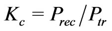 , where
  and
and  are the powers of the signals at the exit of the receiving and the transmitting antennas, respectively. The decoupling coefficient,
  , is inversely related to the value of
 , and is defined as
 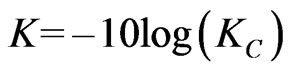 [19]. Minimization of the functional is usually performed by means of non-linear programming and requires the specification of an initial choice for the variation of the impedance distribution,
 . This choice is of great significance because it will influence the number of necessary iteration steps for the minimization of
  in order to reach global and local minima. The closer the initial choice is to the optimized design, the fewer the number of iterations steps. However, to widen the applicability of the results, we chose an initial solution which is nearly arbitrary (given the constraints imposed on the antenna), and work from there towards the optimized design.
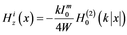
To begin the process of design optimization, we first consider a solution to the two-dimensional design problem for the arrangement shown in Figure 1. On the plane,  , at the point with coordinates
  let an antenna be located which is in the shape of an infinite thread of in-phase magnetic current, directed along
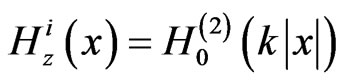
  axis. The opening of a narrow parallel-plate waveguide (Figure 1) can serve as a physical model of such a radiator. This kind of source creates an electromagnetic field in the upper space with a magnetic field vector of intensity:
 , (1)
, (1)
where  is the wave number;
  is the wavelength;
  is the zeroth-order Hankel function of the 2nd kind;
  is the current amplitude; and
  is the characteristic resistance of free space. On the surface
 , the boundary impedance conditions of Shukin-Leontovich are fulfilled:
 . (2)
. (2)
It is necessary to determine the dependence of the passive impedance 
 for a given variation of the magnetic field,
  on the surface
 . Once
  is obtained, the complete field in the upper space is found, and then the degree of decoupling between antennas can be obtained.
2.2. Solution of the Design Optimization Problem
To solve the problem, we use the Lorentz lemma for the upper space in Figure 1. As a result, we obtain the Fredholm integral equation of the second kind relative to the complete field  on the surface
 :
:
 (3)
(3)
where 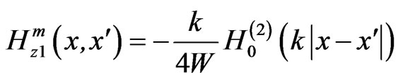 and
and
 is the field of an antenna radiation.
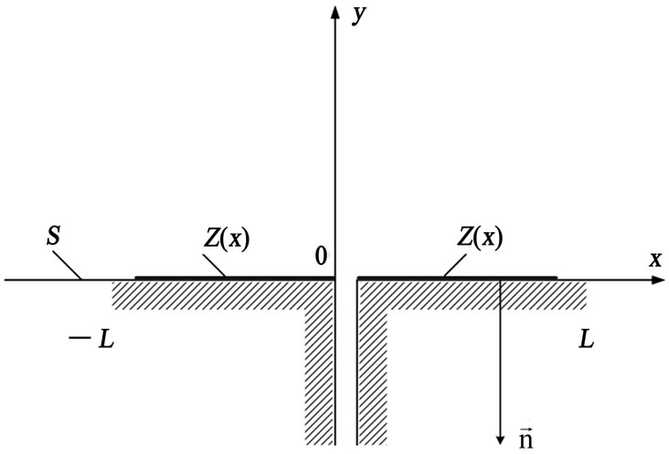
Figure 1. a narrow parallel-plate waveguide with impedance.
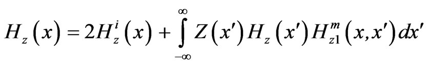
Now, we consider the complete magnetic field on the section  for the entire upper space. From Equation. (3), relative to the complete field,
  , we obtain a Fredholm integral equation of the first kind:
 (4)
(4)
The solution of Equation (4), a complete magnetic field,  , on the final interval
  relative to
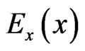 , can be obtained numerically. For example, through the method of Krylov-Bogolyubov [18], the required dependence of the impedance distribution can be found from the boundary conditions of Equation (2),
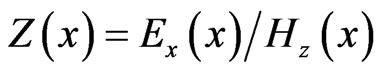 . In this case, the feasibility of the required impedance is not imposed by any limitations and therefore, can be checked in the process of calculation. In this way, we define a category of the passive impedance decoupling structures.
3. Pointwise Synthesis
The problem of the optimization of the design of the complex passive surface impedance is solved in the previous section. The resulting structure gives the complex dependence of the impedance, where its real part is large and positive. The realization of such an impedance with a large real (resistive) part is a complicated task on a planar surface. However, there is another way of achieving a large value of impedance: this can in practice be realized by a corrugated structure with the depth of corrugations divisible approximately by ,
,  , even though such a structure is narrowbanded.
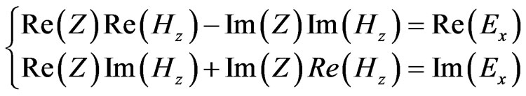
In this section, we consider the variation of antenna decoupling with the help of a purely reactive structure, for which the real part of the synthesized dependence of the complex impedance is simply taken as equal to zero. We assume a weak dependence of tangential components  and
and  on the impedance in Equation (1) and express the boundary impedance conditions, Equation (2), in a complex form:
 (5)
(5)
Then, the solution of the system of equations
 (6)
(6)
can be obtained with the help of the method of linear programming [20-23]. Here, if the real part of the impedance in Equation (6) is set to equal zero (i.e., the resistive impedance , we obtain the minimum deviation of the solution of the system of equations in Equation (6) at each point of the surface of the decoupling structure (such a synthesis is called “pointwise” [20]). This minimum deviation point can be obtained using the exchange method of Stiefel [24]:
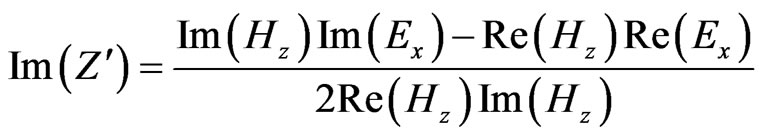 (7)
(7)
In order to look at the behavior of the overall impedance, which is the essence of the exchange method, the relationship between the imaginary and real parts of the impedance is explicitly plotted in Figure 2. The solution of Equation (7) is a point which is equidistant from where the straight lines, given by Equations. (7), where they cross the ordinate axis .
.
4. Results and Discussion
· We state the complete magnetic field on the impedance part, specifying the shape of the field as:
 , (8)
, (8)
where  is the coefficient of attenuation
 .
.
The synthesized impedance must provide sharper EMF attenuation along the structure, as compared with an ideal conducting plane. The attenuation factor is defined by the value of the coefficient . As an example, Figure 3 shows the dependence of the synthesized impedance
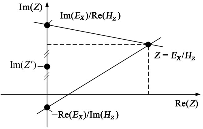
Figure 2. Illustration for the exchange method.
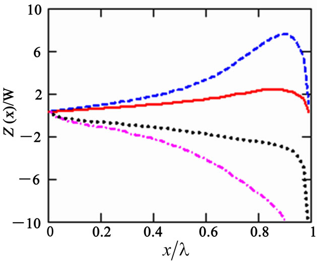
Figure 3. Impedance variations:  (solid and dashed curves) and
  (dotted and dash-dotted curves) for the decay coefficients
  and
and .
.
[ and
and ] for two different coefficients of attenuation, where the length of the impedance structure is
 . It is seen that the real parts of the impedance are positive [
 for
for  (solid) and
  (dashed)] and two imaginary parts are negative (capacitive) [
 for
for  (dotted) and
  (dash-dotted)]. We note here that the impedance has a monotonic increase and the magnitude of the impedance is larger when
 .
.
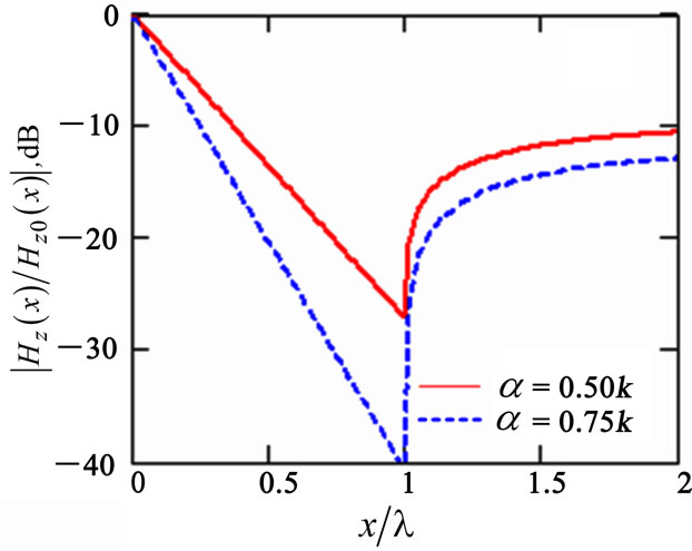
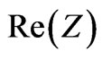
Next, we study the degree of the influence of this impedance on the coupling of antennas. Figure 4(a) shows the dependence of  on the synthesized impedance (Figure 3), normalized relative to the field
  above an ideal conducting plane, for
  (solid curve) and
  (dashed curve). As we can see, a greater attenuation of the field is accompanied by a steeper slope of the impedance alteration, which coincides with the results in the Ref. [18]. The main difference consists in the fact that the impedance obtained in this paper not only has a reactive component but also a resistive component,
 . In order to measure the degree of influence of the resistive part
  of the impedance,
  , on the field attenuation along the impedance structure, we show in Figure 4(b) the De-
 (a)
(a)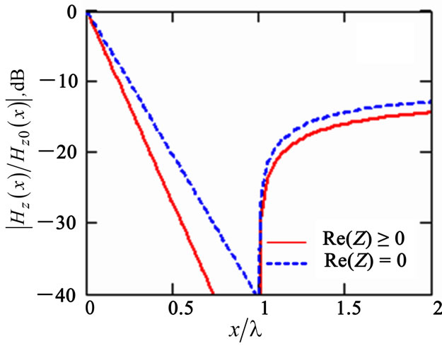 (b)
(b)
Figure 4. (a) Behavior of the field attenuation for the synthesized impedance:  (solid curve) and
  (dashed curve). (b) Behavior of the field attenuation for the synthesized impedance (
 ) with the active component,
  (solid curve), and without it,
  (dashed curve).
pendence of  for the synthesized impedance (
 ), normalized relative to the field
  above an ideal conducting plane, with the active component,
  (solid curve) and without it,
  , (dashed curve). The calculations show that the presence of the resistive part of the impedance not only doesn’t worsen the level of decoupling between antennas, as stated in Ref. [13], but, in fact, increases it by about an additional 5 dB. These results are probably caused by the different dependence of the impedance obtained in this paper compared with what was analyzed in Ref. [13] (this dependence is called uniform). The results of the design optimization show that greater attenuation of the field is reached with a higher rate of impedance growth (generally of its capacitive part, Figure 3). However, the rate of impedance growth (slope of the curves in Figure 4(b)) cannot be arbitrarily large because of practical limitations on the precision of the production of the structures. Therefore, one way to increase the rate of impedance alteration (increase the decoupling) substitutes the monotonically growing impedance with a periodic variation.
Figure 5 shows the dependence of the initial synthesized impedance with , for the structure with length
  (
( , red solid curve and
 , blue dotted curve) and compressed by a factor of three (
 , black dashed curve and
 , purple dash-dotted curve), i.e., with the rate of impedance alteration three times greater. Figure 6 shows the dependence of the field,
  , normalized relative to the field
  above an ideal conducting plane, for the initial impedance (synthesized in Figure 5, solid and dotted curves) and periodic impedance (see Figure 5, dashed and dash-dotted curves). Here, the dash-dotted curve shows the case for homogeneous purely reactive
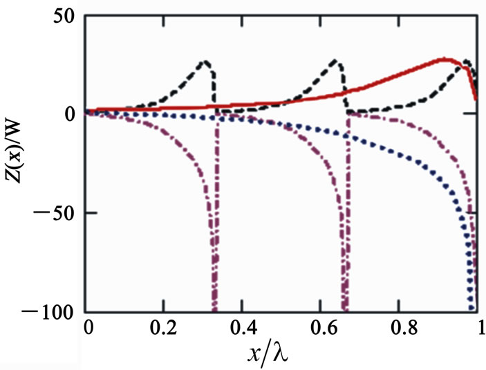
Figure 5. Variation of the initial synthesized impedance with , for the structure with length
  (
( , solid curve and
 , dotted curve) and compressed by a factor of 3, (
 , dashed curve, and
 , dash-dotted curve); i.e., the slope of the impedance variation is 3 times larger.
Figure 6. Solid curve: variation of the field,  , normalized relative to the field,
  , above an ideal conducting plane for the initial impedance (synthesized in Figure 5, solid and dotted curves). Dashed curve: periodical impedance (see Figure 5, dashed and dash-dotted curves). Here, the dash-dotted curve shows the case for homogeneous purely reactive impedance,
 .
.
impedance . As we can see, the level of decoupling grows not monotonically, but at the end of each period, the growth of the coupling coefficient is sharp near the minimum of the impedance, which is characteristic for the propagation of radio waves above non-uniform spreading surfaces [18]. Nevertheless, from comparison of the curves in Figure 6, we can see that the use of several periods of impedance alteration brings an additional gain in the degree of antennas decoupling, 10~40 dB bigger as compared with the monotonic variation (Figure 5, solid and dotted curves). Definitely, the level of the field behind the impedance decoupling structure is defined primarily through the variation of the impedance. Besides, it is evident that the main role is played here by the rate of impedance increase in immediate proximity to the antenna. The results presented in Figure 6 show that from this point of view, the best results are obtained with constant but large capacitive impedance. Nevertheless, in this case, the field along the structure decreases inversely with distance to the 3/2 power. However, the most important thing is that the constant impedance gives the best results outside the impedance structure, i.e., with
 , where the placement of the receiving antenna is assumed.
• We next consider the design optimization of the structure for a given field with the following form:
 (9)
(9)
where  is the coefficient defining the degree of reduction of the overall field intensity on the impedance part of the structure.
Figure 7 shows the variation of the synthesized impedance ( , solid curve and
 , dashed curve) for the structure with the parameters:
  and
and . The behavior of the impedance shows that the
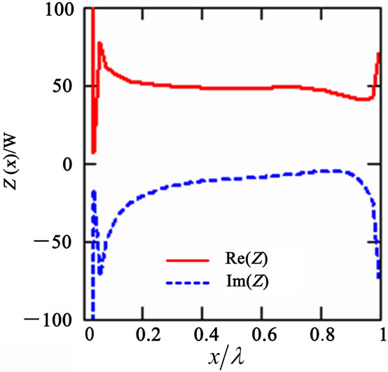
Figure 7. Variation of the synthesized impedance ( , solid curve and
 , dashed curve). The parameters for the calculation are
  and
and .
.
main load in reduction of the field along the structure is carried by the part at the beginning and at the end of the structure, and this does not depend on the length of the structure itself. For example, the dependence of the synthesized impedance distribution for the structure with length  is shown in Figure 8. As the length of the structure increases, the characteristics of the impedance remain the same as in Figure 7. The only difference is that Figure 7 is a compressed version of Figure 8 by a factor of 3 for the length of the structure, with a minor deviation of impedance value.
The real and imaginary values of the impedance are influenced only by the degree of the field reduction on the structure. To demonstrate this fact, we show in Figure 9 the variation of the impedance on the structure with the following parameters:  and
and . When the degree of the field reduction changes from
  (Figure 7) to
  (Figure 9), the real and imaginary values of the impedance are reduced approximately 5 times and 2.6 times smaller, respectively.
In order to see the dependence of the field attenuation on the synthesized impedance, we plot 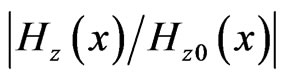 as a function of
  in Figure 10. The solid curve
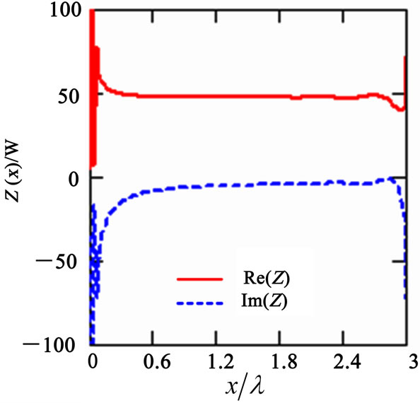
Figure 8. Variation of the synthesized impedance ( , solid curve and
 , dashed curve) with the length
 .
.
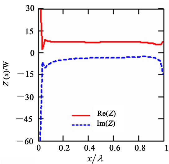
Figure 9. Variation of the synthesized impedance ( , solid curve and
 , dashed curve) with the following parameters:
  and
and .
.
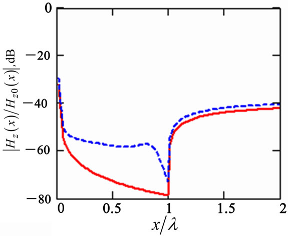
Figure 10. Behavior of the field attenuation relative to Figure 7 (solid curve) and with a purely reactive impedance,  , (dashed curve).
corresponds to the impedance distribution (both  and
and , shown in Figure 7) and the dashed curve with the purely reactive impedance
 . This result indicates that the prevailing role in the reduction of the level of the complete field behind the impedance structure is played by the reactive part of impedance. The presence of an active component leads to an additional decrease of the field behind the structure, making it 3~5 dB smaller.
We notice from the behavior of the curves in Figures 7-9 that the main load falls on the initial and final parts of the structure, (the so-called “take off” and “landing” grounds of the structure [25]). To confirm this, we design a structure with zero impedance on its initial and final parts, shown in Figure 11, where the parameters are used for  and
and . Figure 12 shows the dependence of
  on the impedance distribution for a structure with zero impedance on its initial part (at the distances
  and
and , solid curve), and with zero impedance on its final part (at the distances
  and
and , dashed curve). For the comparison, the dash-dotted curve corresponds to the pure impedance structure. The calculations show that the main role in providing decoupling between antennas belongs to the initial part (the “take off” stripe), directly

Figure 11. Synthesis of structures with zero impedance on their initial and final sections. The parameters for the calculation are  and
and .
.
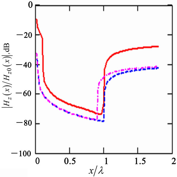
Figure 12. Behavior of the field attenuation for the variation of the synthesized impedance structures with zero impedance on its initial section (at the distances  and
and , solid curve) and with zero impedance on its final part (at the distances
  and
and 
 , dashed curve). For comparison, the dash-dotted curve corresponds with the pure impedance structure.
touching the opening of the transmitting antenna. The impact of the final part in providing decoupling is much less. In addition, the “take off” stripe defines not only the level of the complete field above the impedance structure but also behind it, where the placement of the receiving antenna is assumed. At the same time, the presence of the ideal conducting part, even if it is very small , leads to sharp growth in the value of the complex impedance of the structure. This, in turn, makes its practical realization more difficult. This statement applies also for any length of the structure. We note that increasing the length of the impedance structure causes a significant reduction of the field only on the structure itself, but this reduction is much smaller behind it.
Finally, we consider the method of pointwise synthesis. The distributions of reactive impedance and the variation of  for the designed structure are shown in Figures 13 and 14, respectively, with the same parameters as in Figure 7, where the active part of the impedance is taken to be equal to zero (solid curves) and the structure with reactance is calculated by Equation (7)

Figure 13. Variation of the reactive impedance relative to the initial impedance (solid curve) and the optimized impedance (dashed curve) in accordance with Equation (7). The parameters are the same as in Figure 7.
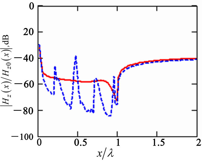
Figure 14. Behavior of the field attenuation for the structure, in which after the solution of the problem of synthesis, the active part of the impedance is set equal to zero (solid curves) and for the structure with reactance calculated by Equation (7) (dashed curves). The reactance optimized in accordance with Equation (7) (Figure 13, dashed curve) completely differs from the initial calculation (Figure 13, solid curve) because in it, the capacitive impedance along with the inductive impedance has emerged. The parameters are the same as in Figure 7.
(dashed curves). The impedance of the reactance optimized in accordance with Equation (7) (Figure 13, dashed curve) differs completely from the initial calculation (Figure 13, solid curve), because in it, the capacitive impedance along with the inductive impedance has emerged. We obtain more detail in the behavior of the complete field on the impedance part of the structure. In Figure 14, behavior of the field attenuation for the structure, in which after the solution of the problem of synthesis, the active part of the impedance is set equal to zero (solid curves) and for the structure with reactance calculated by Equation (7) (dashed curves). The alternating character of the impedance distribution suggests that a structure which realizes it (for example, a corrugated one) will turn out to be more broadband. Common to all calculations was the large negative reactance near the opening of the transmitting antenna.
The reactance given in Equation (7) has a dependence similar to the function, . A similar form of the impedance (reactance) distribution was obtained in Ref. [26], where the authors considered the design optimization of an impedance plane, transforming the cylindrical front of the wave of a linear source into the front of the heterogeneous flat wave reflected in a given direction. This similarity encourages the use of the results of this paper in the interest of decoupling antennas.
5. Conclusions
In summary, we have solved the problems of the optimization of the design of a complex passive surface impedance for a given electromagnetic field distribution and by means of pointwise synthesis, with the purpose of thereby creating optimized decoupling structures. We present different variations of the field along the impedance structure. We have shown that a greater attenuation of the field is accompanied with a greater degree of impedance variation and that the use of several periods of impedance variation brings an additional gain in the amount of antenna decoupling. We also calculate the degree of influence of the resistive part of the impedance on the rate of the field attenuation along the impedance structure. Finally, we notice that the most efficient way of reducing mutual coupling between antennas located on the same plane is the placement of the impedance structure with a large value of reactive impedance near the transmitting antenna. However, during the solution of the design optimization, the interaction between antennas was not taken into account. It is evident that the presence of the receiving aperture antenna will lead to undesirable reduction of antenna decoupling by means of the heterogeneous character created by the aperture of the receiving antenna. Future research will investigate this question as well.
The derived impedance variation can be used as an independent solution of the problem of providing electromagnetic compatibility, as well as the first step in further optimization of the structure with the help of non-linear programming methods.
6. Acknowledgements
One of the authors (J.-F. D. Essiben) wishes to thank Professor Yu. V. Yukhanov from the Taganrog Institute of Technology at the Southern Federal University in Russia for helpful discussions.
REFERENCES
- G. Goussetis, A. P. Feresidis and J. C. G. Apostolopoulos, “Periodically Loaded 1-D Metallodielectric Electromagnetic Bandgap Structures for Miniaturization and Bandwidth Enhancement,” IEE Proceedings of Microwave Antennas Propagation, Vol. 151, No. 6, 2004, pp. 481- 484. doi:10.1049/ip-map:20040814
- C. C. Chiau, X. Chen and C. Parini, “Multiperiod EBG Structure for Wide Stopband Circuits,” IEE Proceedings of Microwave Antennas Propagation, Vol. 150, No. 6, 2003, pp. 489-492. doi:10.1049/ip-map:20031087
- N. C. Karmakar and M. N. Mollah, “Potential Applications of PBG Engineered Structures in Microwave Engineering: Part I,” Microwave Journal, Vol. 47, No. 7, 2004, pp. 22-44.
- B. I. Rumsey, Z. Popovic and M. P. May, “Surface-Wave Guiding Using Periodic Structures,” IEEE APS-International Symposium Digest, Salt Lake City, 17-21 July 2000, pp. 342-345.
- D. Sievenpiper and E. Yablonovitch, “Eliminating Surface Currents with Metallodielectric Photonic Crystals,” IEEE International Microwave Symposium Digest, Baltimore, 7-12 June 1998, pp. 663-666.
- D. Sievenpiper, L. Zhang, R. F. J. Broas, N. G. Alexopolous and E. Yablonovitch, “High-Impedance Electromagnetic Surfaces with a Forbidden Frequency Band,” IEEE Transactions on Microwave Theory and Techniques, Vol. 47, No. 11, 1999, pp. 2059-2074. doi:10.1109/22.798001
- K. C. Chen, C. K. C. Tzuang, Y. Qian and T. Itoh, “Leaky Properties of Microstrip above a Perforated Ground Plane,” IEEE International Microwave Symposium Digest, Anaheim, 13-19 June 1999, pp. 69-72.
- A. Freni, C. Mias and R. L. Ferrari, “Hybrid Finite-Element Analysis of Electromagnetic Plane Wave Scattering from Axially Periodic Cylindrical Structures,” IEEE Transactions on Antennas and Propagation, Vol. 46, No. 12, 1998, pp. 1859-1866. doi:10.1109/8.743824
- P. S. Kildal, A. A. Kishk and A. Tengs, “Reduction of Forward Scattering from Cylindrical Objects Using Hard Surfaces,” IEEE Transactions on Antennas and Propagation, Vol. 38, No. 10, 1990, pp. 1537-1544. doi:10.1109/ 8.59765
- S. Benenson and A. I. Kurkchan, “Decoupling of Antennas by Means of Periodic Structures,” Radiotechnics and Electronics, Vol. 37, No. 12, 1995, pp. 77-89.
- K. K. Belostotskaya, M. A. Vasilyev and V. M. Legkov, “Spatial Decoupling between Antennas on Big Size Solids,” Radiotechnics, Vol. 41, No. 10, 1986, pp. 77-79.
- V. N. Lavrushev and Y. E. Sedelnikov, “Construction of Antennas Taking into Account Decoupling Requirements,” Transactions of Higher Education Institutions, Radio Electronics, Vol. 23, No. 2, 1980, pp. 31-38.
- V. V. Martsafey and I. G. Shvayko, “Influence of Corrugated Structures on Interaction of Near-Omnidirectional Antennas,” Transactions of Higher Education Institutions, Radio Electronics, Vol. 24, No. 5, 1981, pp. 18-22.
- A. V. Kashin and V. I. Solovyov, “Research of SmallSized on Interaction of Near-Omnidirectional Antennas, Located on a Circular Cylindrical Surface,” Transactions of Higher Education Institutions, Radio Electronics, Vol. 25, No. 2, 1982, pp. 78-80.
- Y. L. Lomukhin, S. D. Badmayev and N. B. Chimindorzhiev, “Decoupling of Antennas by the Edge of Conducting Semi-Plane,” Radiotechnics, Vol. 40, No. 8, 1985, pp. 47-50.
- V. V. Martsafey and M. A. Solodovnikov, “Synthesis of Near-Omnidirectional Antenna with an Increased Electromagnetic Compatibility,” Transactions of Higher Education Institutions, Radio Physics, Vol. 23, No. 10, 1980, pp. 1250-1255.
- A. G. Kurkchan, “Coupling between Antennas in the Presence of Corrugated Structures,” Radiotechnics and Electronics, Vol. 22, No. 7, 1977, pp. 1362-1373.
- O. N. Tereshin, V. M. Sedov and A. F. Chaplin, “Synthesis of Antennas on Decelerating Structures,” Communication Press, Moscow, 1980.
- Y. S. Joe, J.-F. D. Essiben and E. M. Cooney, “Radiation Characteristics of Waveguide Antennas Located on the Same Impedance Plane,” Journal of Physics D: Applied Physics, Vol. 41, No. 12, 2008, pp. (125503)1-11.
- V. G. Sharvarko, “Pointwise Synthesis in the Inverse Task of Scattering for an Impedance Cylinder,” Scattering of Electromagnetic Waves, Taganrog, Vol. 44, No. 1, 1975, pp. 71-96.
- B. M. Petrov and V. G. Sharvarko, “Inverse Problem of Diffraction for an Impedance Cylinder,” Transactions of Higher Education Institutions, Radio Electronics. Vol. 18, No. 12, 1975, pp. 90-93.
- V. G. Sharvarko, “About the Realized Diagrams in Inverse Problem of Scattering for an Impedance Cylinder,” Scattering of Electromagnetic Waves, Taganrog, Vol. 44, No. 1, 1975, pp. 87-96.
- B. M. Petrov and V. G. Sharvarko, “Approximated Solutions of Inverse Problem of Scattering for a Circular Impedance Cylinder,” Scattering of Electromagnetic Waves, Taganrog, Vol. 41, No. 1, 1976, pp. 11-24.
- E. L. Stiefel, “Über Diskrete Undlineare Tscheby-ScheffAppproximation,” Numerische Mathematik, Vol. 1, 1959, pp. 1-28. doi:10.1007/BF01386369
- G. P. Grudinskaya, “Propagation of Radio Waves,” Higher School Press, Moscow, 1975.
- A. Y. Yukhanov, “Two-Dimensional Task of Impedance Plane Synthesis,” Radio Engineering Circuits, Signals and Devices, Taganrog, Vol. 45, 1998, pp. 92-95.