Smart Grid and Renewable Energy
Vol.4 No.6(2013), Article ID:36569,7 pages DOI:10.4236/sgre.2012.46049
Partial Shading of PV System Simulation with Experimental Results
![]()
Department of Electrical Engineering, Palestine Technical University-Kadoorie, Tulkarm, Palestine.
Email: b.alsayid@ptuk.edu.ps, samer_sadi@yahoo.com, Eng.jafar2012@hotmail.com, mohamaddradi@yahoo.com
Copyright © 2013 Basim A. Alsayid et al. This is an open access article distributed under the Creative Commons Attribution License, which permits unrestricted use, distribution, and reproduction in any medium, provided the original work is properly cited.
Received June 11th, 2013; revised July 11th, 2013; accepted July 19th, 2013
Keywords: Partial Shading; Modeling; Simulation; Bypass Diodes
ABSTRACT
In a solar photovoltaic array, it is possible that shadow may fall over some of its cells. Under partial shading conditions the PV characteristic gets more complex with multiple peaks. The purpose of this paper is to illustrate, by analyzing different shading situations, the effects that partial shading can cause in a PV array. First this is done by simulation using Matlab/Simulink, then the impact of shading is illustrated experimentally by measurements on a two commercial 140 W PV panels series connected.
1. Introduction
Photovoltaic modules are connected in series and parallel to form a PV array in order to match the power requirements in terms of voltage and current [1,2]. The total power in such an array is, however lower than the sum of the individual rated power of each module. There are different reasons for that. The main reason, which is the purpose of this paper is partial shading [3,4]. In a series connected solar photovoltaic module, performance is adversely affected if the cells are not equally illuminated. All the cells in a series array are forced to carry the same current even though a few cells under shade produce less photon current. The shaded cells may get reverse biased, acting as loads, draining power from fully illuminated cells. If the system is not appropriately protected, hotspot problem can arise and in several cases, the system can be irreversibly damaged. The PV plants are built today in a fixed series-parallel configuration and the single module is equipped with bypass diodes included in different configurations. This is used to bypass the single module when it is slightly radiated in order to avoid that the single module current may reduce the current of the whole photovoltaic array. On one hand this solution is easily adoptable and allowed to improve the energy production from the whole PV array but on the other hand it imposes to renounce to the energy produced by the module which is bypassed by the diode [5]. The purpose of this paper is to illustrate, by analyzing different shading situations, the effects that partial shading can cause in a PV array [6]. First this is done by simulation using Matlab/Simulink, then the impact of shading is illustrated experimentally by measurements on a two commercial PV panels series connected.
2. Partial Shading and Bypass Diodes
Uniform illumination intensity in a panel is not almost satisfied because of buildings or trees shades, atmosphere fluctuation, existence of clouds and daily sun angle changes. Shade impact depends on module type, fill factor, bypass diode placement severity of shade and string configuration. Power loss occurs from shade, also current mismatch within a PV string and voltage mismatch between parallel strings [7]. Typically, a crystalline silicon module will contain bypass diodes to prevent damage from reverse bias on partially shaded cells. These diodes are placed across 12 - 18 cells in a group of cells.
In Figure 1 is shown a module with 36 cells connected in series like the ones used in this research, each consisting of 2 groups of 18 cells. Each group of cells is connected to a bypass diode that begins conducting if shading causes a cell to go far enough into reverse bias. In this example, shade causes diode D2 to short out its group of cells, reducing module 1’s voltage by 1/2.
The bypass diode across this group of cells will begin conducting when shading causes a cell to go far enough into reverse bias. The bypass diode allows current from
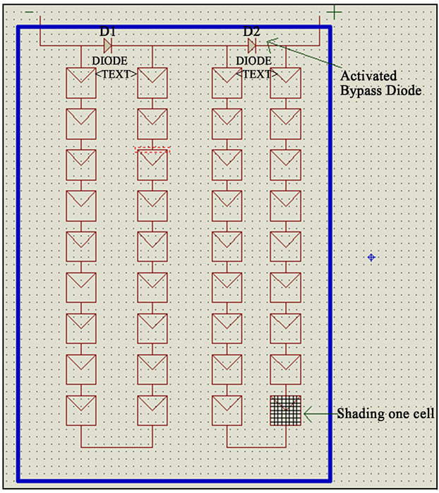
Figure 1. Single module with 36 cells in series.
non-shaded parts of the module to pass by the shaded part and limits the effect of shading to the only neighboring group of cells protected by the same bypass diode. When a bypass diode begins conducting, the module voltage will drop by an amount corresponding to the sum of cell voltages protected by the same bypass diode plus the diode forward voltage, but current from surrounding un-shaded groups of cells continues around the group of shaded cells. The effect of shade on power output of typical PV installation is nonlinear in that a small amount of shade on a portion of an array can cause a large reduction in output power [8-10].
3. Partial Shading Simulation of a Single Module
In Table 1 are shown the electrical characteristics of the modules used in this research under standard test conditions (STC) which means the irradiance G = 1000 W/m2, temperature = 25˚C and AM = 1.5. It can be seen that the module consists of two groups series connected. Each group consists of 18 cells connected in series. A bypass diode is connected in antiparallel with each group [11].
In Figure 2 is shown the simulation of a single module based on the single diode model equations implemented in Matlab/Simulink. The simulation allows to modify the environmental data and the characteristic parameters of the implemented photovoltaic module such as irradiance, temperature, short circuit current, open circuit voltage, etc.
Three cases has been simulated .The first case is under STC without shading for Group 1 and Group 2. The simu
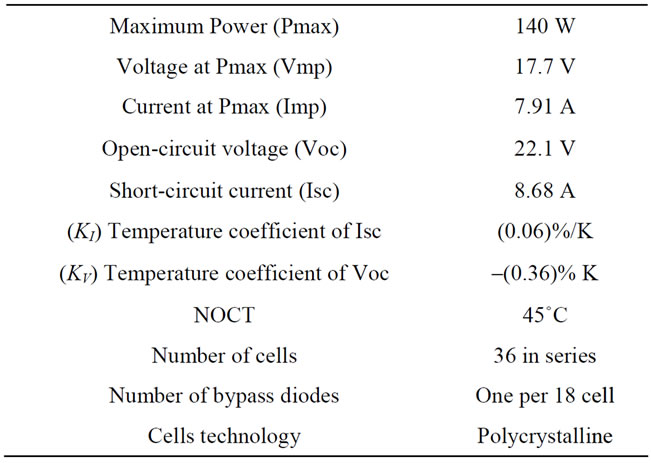
Table 1. Electrical characteristics data of the Kyocera solar KD140GH-2PU at 25˚C, 1.5 AM, 1000 W/m2. (taken from the datasheet)
lation resulting V-I characteristic (red curve) is shown in Figure 3. The short circuit current is very closed to 8.68 A and the Voc is very closed to 22.1 V. The resulting P-V characteristic (red curve) is shown for the same case in Figure 3. The maximum power is 140 W which is the expected value. Vmp is very closed to the value 17.7 V and Imp is very closed to the value 7.91 A. The second case is simulated for irradiance (G = 1000 W/m2) on Group 1 and shading on Group 2 (G = 500 W/m2) with two bypass diodes connected. In Figure 3 the resulting V-I characteristic is shown (green curve). In Figure 3 the resulting P-V characteristic (green curve) is shown. As the two groups are not equally illuminated the power contributed by each group is different and the maximum power is less than 140 W. The presence of bypass diodes will allow the un-shaded cells in a group to conduct their maximum current at a given irradiance and temperature (the green curve). Figures 3 and 4 reveal that, under partially shaded conditions, the bypass diodes introduce multiple steps in the I-V characteristics and multiple peaks in the P-V characteristics.
The third case is as in the second case but with the bypass diodes disconnected. In Figure 3 the resulting V-I characteristic is shown (blue curve). In Figure 4 is shown the resulting P-V characteristics (blue curve). If the bypass diodes are not present, the shaded group will limit the current output of the un-shaded group (blue curve).
The following two cases have been simulated to make comparison with the experimental measurements made for the same conditions. In Figure 5 is shown the resultant I-V characteristic and in Figure 6 is shown the P-V characteristic for irradiance G = 922 W/m2 and T = 61˚C without shading. Voc value is 19.5 V, Isc is 8 A and Pmax is 108 W.
In Figure 7 is shown the resultant I-V characteristic and in Figure 8 is shown the P-V characteristic for ir-
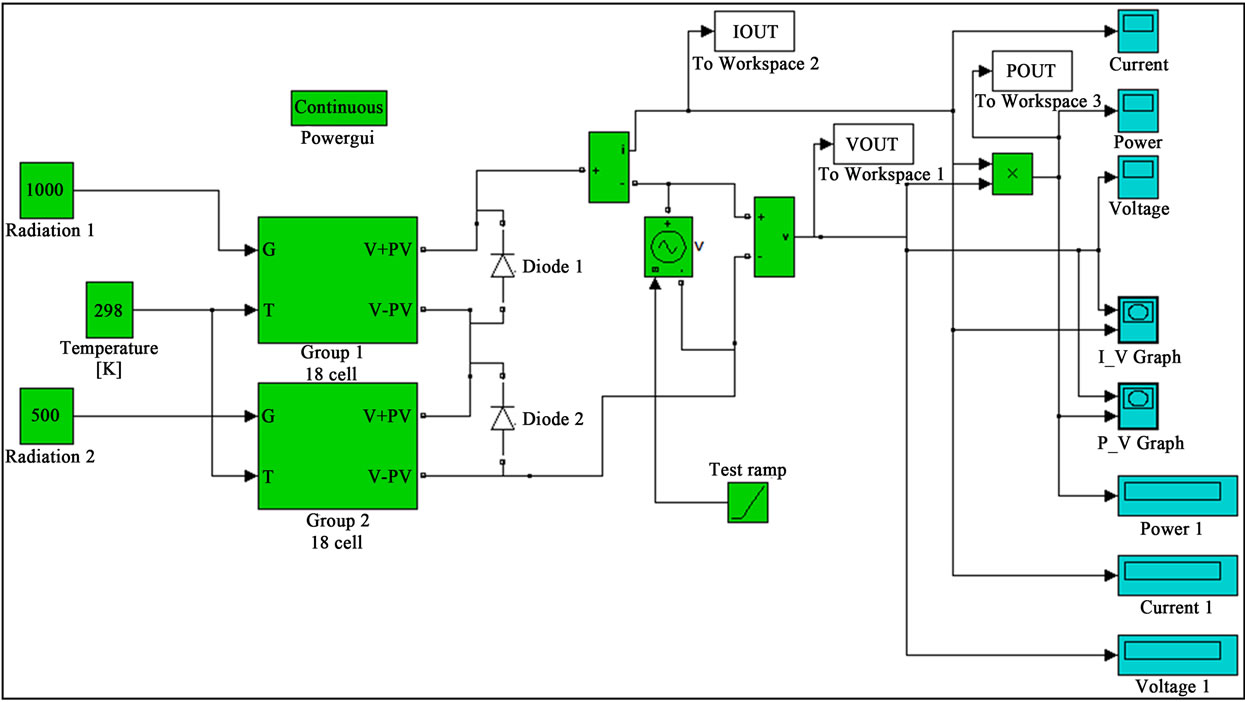
Figure 2. Simulation of a single module 36 cells with one bypass diode per 18 series connected cells.
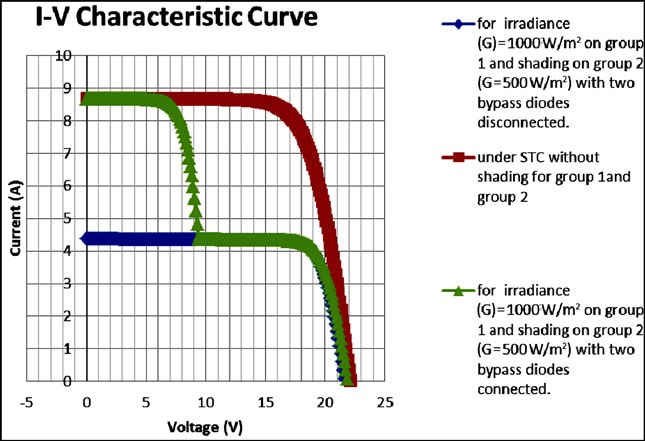
Figure 3. I-V Characteristic curves of single module for 3 different conditions.
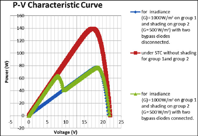
Figure 4. P-V Characteristic curves of single module for 3 different conditions.
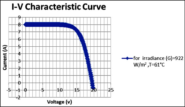
Figure 5. I-V characteristics of single module simulated for G = 922 W/m2, T = 61˚C.
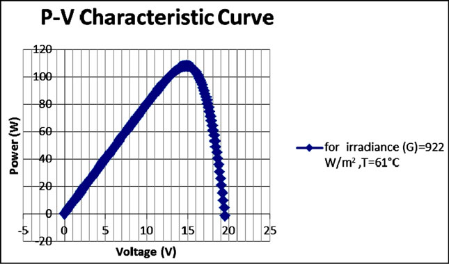
Figure 6. P-V characteristics of single module simulated for G = 922 W/m2, T = 61˚C.
radiance G = 926 W/m2 for non-shaded group and G = 193 W/m2 for the shaded one, T = 61˚C. Voc value is 18.9 V, Isc is 8 A and Pmax is 48.4 W.
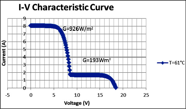
Figure 7. I-V characteristics of single module simulated for G = 926 W/m2, G = 193 W/m2, T=61˚C.
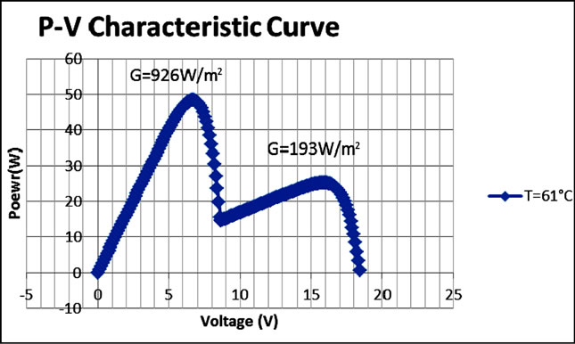
Figure 8. P-V characteristics of single module simulated for G = 926 W/m2, G = 193 W/m2, T = 61˚C.
4. Partial Shading Simulation of Two Series-Connected Modules
When the PV modules are connected in series, they will conduct the same current but the voltage across them will be different.
These voltages are added together to determine the resultant output voltage. In Figure 9 is shown the simulation of two identical modules connected in series. The first module, as said before is 36 cells, is composed of Group 1 and Group 2. The second module is composed of Group 3 and Group 4. The two groups are connected in series.
Three cases has been simulated .The first case is under STC without shading for Group 1, Group 2, Group 3 and Group 4. In Figure 10 the simulation resulting V-I characteristic (red curve) of the two modules in series is shown. The short circuit current is 8.68 A and the Voc is 44.2 V. In Figure 11 the resulting P-V characteristic (red curve) is shown. The maximum power in this case is 280 W which is the sum of the power of the two modules equally illuminated. The second case is for irradiance G = 1000 W/m2 on Group 1 and with shading (G = 500 W/m2) only on Group 2. The four bypass diodes are connected. In Figure 10 the resulting V-I characteristic is shown (green curve).
In Figure 11 the resulting P-V characteristic (green curve) is shown. As the two modules are not equally illuminated the power contributed by each panel is different and the maximum power is less than 280 W. The third
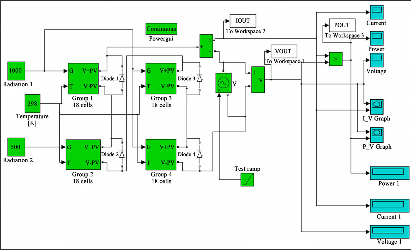
Figure 9. Simulation of two modules in series.
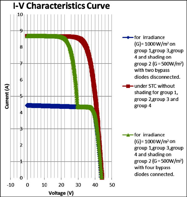
Figure 10. V-I characteristics of two modules in series.
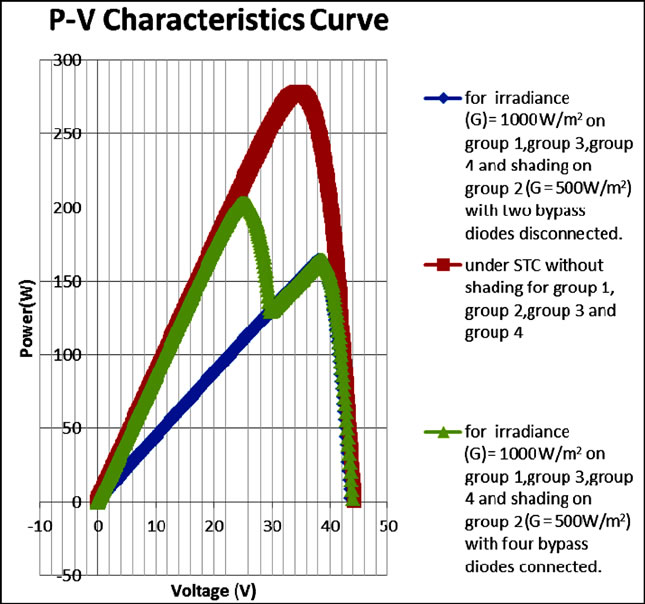
Figure 11. P-V characteristics of two modules in series.
case is as in the second case but with the bypass diodes disconnected. In Figure 10 the resulting V-I characteristic is shown (blue curve). In Figure 11 is shown the resulting P-V characteristics (blue curve).
The following case has been simulated to make comparison with the experimental measurements obtained. In Figure 12 is shown the resultant I-V characteristic and in Figure 13 is shown the P-V characteristic for irradiance G = 901W/m2 for the non-shaded groups, G = 185 W/m2 for the shaded one and T = 61˚C. Voc value is 38 V, Isc is 7.84 A and Pmax is 152.6 W. It is seen that the current is low for the shaded group because of the low irradiance.
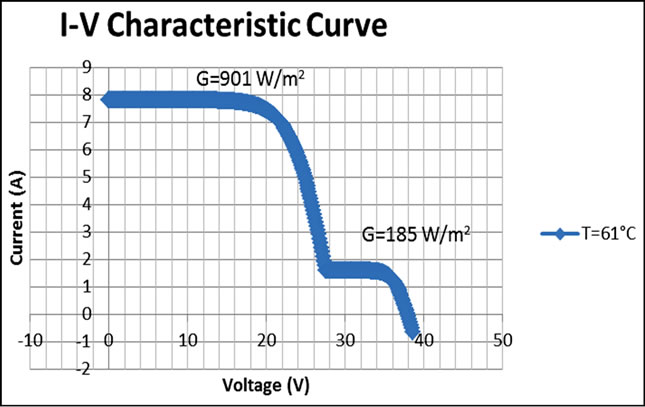
Figure 12. I-V characteristics of two modules in series simulated for G = 901 W/m2, G = 185 W/m2, T = 61˚C.
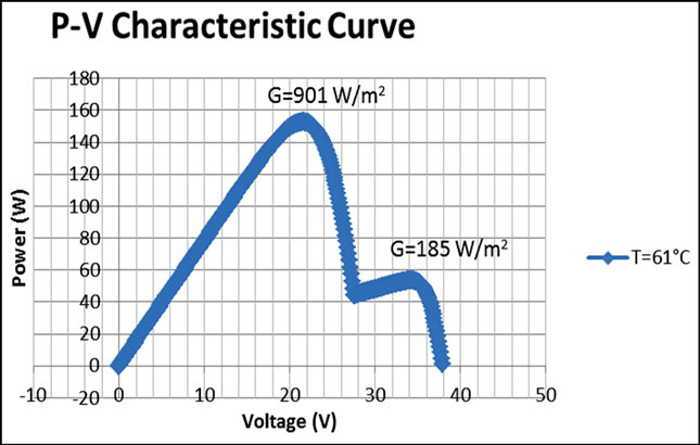
Figure 13. P-V characteristics of two modules in series simulated for G = 901 W/m2, G = 185 W/m2, T = 61˚C.
5. Experimental Measurements
A number of experimental measurements has been done to study the impact of partial shading on the PV system and to verify the validity of the simulation. The instrument used for this purpose is HT I-V 400 Tracer.
The first group of measurements has been done on a single module as shown in Figure 14.
In Figure 15 are shown I-V and P-V characteristics of a single module obtained experimentally for G = 922 W/m2, T = 61˚C without shading. Voc value is 19.62 V, Isc is 7.88 A and Pmax is 110.48 W. In Figure 16 are shown I-V and P-V characteristics of a single module obtained experimentally for G = 926 W/m2 for the non-shaded group, G = 193 W/m2 for the shaded one and T = 61˚C. Voc value is 19.62 V, Isc is 7.68 A and Pmax is 49.15 W.
In Figure 17 is shown the PV system of two modules connected in series. In Figure 18 are shown I-V and P-V characteristics for two modules in series without shading for G = 896 W/m2, T = 61˚C.
In Figure 19 is shown the same system of Figure 17 with shading of one cell. In Figure 20 are shown I-V and P-V characteristics for two modules in series for G = 901 W/m2 for the non-shaded groups, G = 185 W/m2 for the
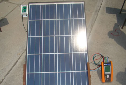
Figure 14. Single module PV system.
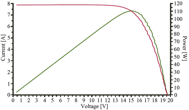
Figure 15. V-I, P-V characteristics of single module obtained experimentally without shading, G = 922 W/m2, T = 61˚C.
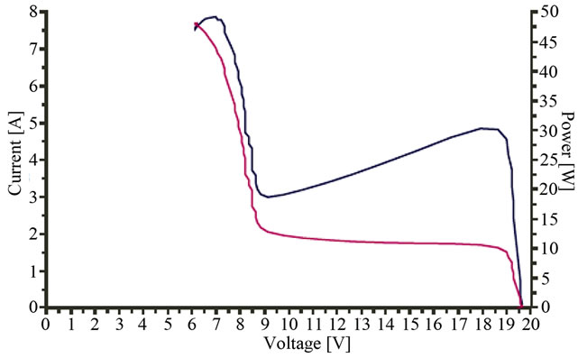
Figure 16. V-I , P-V characteristics of single module obtained experimentally, G = 926 W/m2 for non-shaded group, G = 193 W/m2 for the shaded group, T = 61˚C.
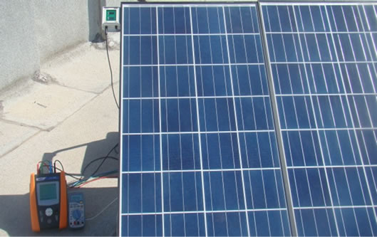
Figure 17. PV system of two modules connected in series.
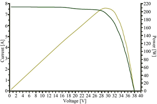
Figure 18. I-V, P-V characteristics of two modules connected in series obtained experimentally for G = 896 W/m2, T = 61˚C without shading.
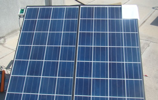
Figure 19. PV system of two modules connected in series with shading.
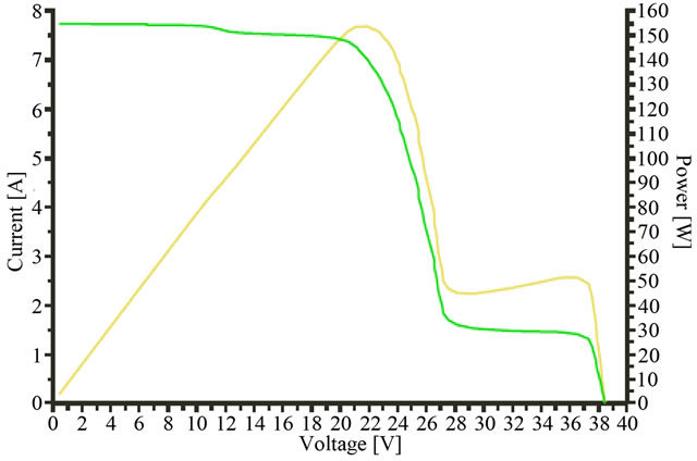
Figure 20. I-V, P-V characteristics of two modules connected in series obtained experimentally with shading.
shaded one and T = 61˚C. Voc value is 38.5 V, Isc is 7.74 A and Pmax is 153.7 W.
In Figure 21 are shown the I-V and P-V characteristics obtained experimentally for shading completely half module. For non-shaded cells G = 901 W/m2, T = 61˚C. Voc value is 33.5 V, Isc is 7.75 A and Pmax is 153.81 W.
In Figure 22 are shown the I-V and P-V characteristics of two series connected modules with complete shad-
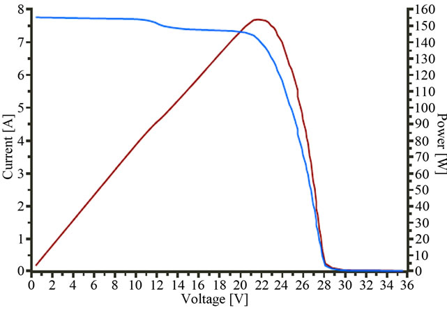
Figure 21. I-V, P-V characteristics of two modules connected in series obtained experimentally with shading.
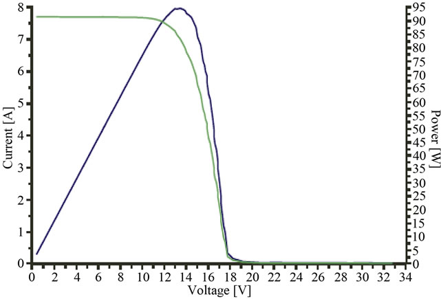
Figure 22. V-I, P-V characteristics obtained experimentally with shading completely one module, for non-shaded cells G = 898 W/m2, T = 61˚C.
ing for one module, the non-shaded module has G = 898 W/m2 and T = 61˚C.
6. Conclusion
MATLAB/SIMULINK software has been developed to simulate the behavior of PV modules with different configurations under variable meteorological conditions, in particular the impact of partial shading. The effect of the bypass diodes on PV characteristics under partially shaded conditions has been simulated. Experimental measurement has been done and the validity of the simulation software has been verified.
7. Acknowledgements
The authors would like to thank Palestine Technical University-Kadoorie for supporting this research and allowing us to conduct this work in the university labs.
REFERENCES
- S. Shah, S. Chauhan and H. M. Rai, “Characteristics of PV Array Used for Distributed Power Generation-Modelling and Simulation,” International Journal on Emerging Technologies, 2010, pp. 61-66.
- R. Ramaprabha and B. I. Mathur, “Impact of partial Shading on Solar pv Module Containing Series Connected Cells,” International Journal of Recent Trends in Engineering, Vol. 2, No. 7, 2007, pp. 56-60.
- D. Sera and Y. Baghzouz, “On the Impact of Partial Shading on PV Output Power,” WSEAS/IASME International Conference on Renewable Energy Sources, 2008.
- B. Koirala, B. Sahan and N. Henze, “Study on MPP Mismatch Losses in Photovoltaic Applications,” European Photovoltaic Solar Energy Conference and Exhibition (EU PVSEC) Hamburg, Fraunhofer, 2009, pp. 3727-3733.
- V. Di Dio, D. La Cascia and R. Micelli, “A Mathe-Matical Model to Determine the Electrical Energy Production in Photovoltaic Fields under Mismatch Effect,” 2009 International Conference on Clean Electrical Power, Capri, 9-11 June 2009, pp. 46-51.
- M. C. Alonso-Garcia, J. M. Ruiz and W. Herrmann, “Computer Simulation of Shading Effects in Photovoltaic Arrays,” Renewable Energy, 2006, pp. 1986-1993.
- A. Kajihara and T. Harakawa, “Model of Photovoltaic Cell Circuits under Partial Shading,” IEEE International Conference on Industrial Technology, Hong Kong, 14-17 December 2005, pp. 886-870.
- C. Deline, “Partially Shaded Operation of a Grid-Tied pv System,” 34th IEEE Photovoltaic Specialists Conference, Philadelphia, 7-12 June 2009.
- M. S. Ngan and C. W. Tan, “Multiple Peak Tracking Algorithm Using Particle Swarm Optimization Incorporated with Artificial Neural Network,” World Academy of Science, Engineering and Technology, 2011, pp. 379-385
- E. Diaz-Dorado, A. Suarez-Garcia, C. Carrillo and J. Cidras, “Influence of the Shadows in Photovoltaic Systems with Different Configurations of Bypass Diodes,” 2010 International Symposium on Power Electronics Electrical Drives Automation and Motion (SPEEDAM), Pisa, 14-16 June 2010, pp 134-139.
- H. Patel and V. Agarwal, “Matlab-Based Modelling to Study the Effects of Partial Shading on pv Array Characteristics,” IEEE Transactions on Energy Conversion, Vol. 23, No. 1, 2008, pp. 302-310. doi:10.1109/TEC.2007.914308