Energy and Power Engineering
Vol. 4 No. 5 (2012) , Article ID: 22836 , 9 pages DOI:10.4236/epe.2012.45041
Design and Analysis of a 24 Vdc to 48 Vdc Bidirectional DC-DC Converter Specifically for a Distributed Energy Application
1Mindanao University of Science and Technology, Cagayan de Oro City, Philippines
2University of Massachusetts Lowell, Lowell, USA
Email: acultura2003@yahoo.com, ziyadsalameh@uml.edu
Received July 19, 2012; revised August 20, 2012; accepted August 31, 2012
Keywords: Distributed Energy Resources; Bidirectional DC-DC Converter; ELECTRIC Grid
ABSTRACT
The design of a bidirectional DC-DC power converter specifically for a distributed energy application is presented. The existing two different DC voltage battery bank of the distributed generation needs to interlink each other using a bi-directional DC-DC converter in order to minimize the unbalance of the output load currents of the three inverters connected to electric grid system. Through this connection, a current can flow from one system to another or vice versa depending on which systems need the current most. Thus, unbalanced currents of the grid line have been minimized and the reliability and performance of the DER grid connected system has been increased. A detailed mathematical analysis of the converter under steady state and transient condition are presented. Mathematical models for boost and buck modes are being derived and the simulink model is constructed in order to simulate the system. Moreover, the model has been validated on the actual operation of the converter, showing that the simulated results in Matlab Simulink are consistent with the experimental ones.
1. Introduction
The distributed energy resources (DER) considered in this study is composed of photovoltaics (PV), wind turbines, a fuel cell, batteries and supercapacitors. The system is divided into two subsystems. Subsystem 1 is composed of PV, a PEM fuel cell, wind turbines and 24 V batteries. Subsystem 2 is composed of PV, a wind turbine, supercapacitor and 48 V batteries. The detailed schematic diagram of grid connected DER at the University of Massachusetts Lowell (UMass Lowell) is presented in Figure 1. This DER, as it stands now, consists of four roof top mounted wind turbines rated for 2.4 kW, 1.5 kW, 500 W, and 300 W; two photovoltaic arrays rated for 2.5 kW and 10.56 kW that are connected through a microprocessorcontrolled maximum power point trackers (MPPT); two battery storage banks rated at 24 V, 45 kWh and 48 V, 30 kWh; a 1.2 kW PEM type fuel cell; four modules of Maxwell Super capacitors, each of which is rated at 48 V, 140 Farads; and three 4 kW sine wave inverters that are connected to the utility grid. A data acquisition system (DAQ) is installed in order to monitor the performance of all energy resources.
In its operation, there are times that the 24 V battery bank supplies less current to Inverter 1 than the 48 V battery bank supplies to Inverters 2 and 3. This causes an imbalance of currents to the 3-phase electric grid. There are also times that Inverter 1 or 2 shuts-down or malfunctions. In other words, the quality, the reliability and the performance of the system are compromised. Hence, integrating the two systems can lessen or resolve this problem. So, there was a need for the design and construction of a bidirectional DC-DC converter. This bidirectional DC-DC converter would connect the two-battery banks of the distributed energy resources. Through this connection, a current would flow from one system to another depending on which system needed the current the most. Imbalanced currents of the grid line would be minimized, and the reliability and performance of the existing DER grid connected system would increase. The author designed the power and control circuit for this bidirectional DCDC converter and it is suited to this use. The mathematical analysis, simulink model and simulation results are presented here and a prototype was fabricated and tested.
2. System Design
Figure 2 illustrates the power circuit configuration of a bidirectional DC-DC converter that was installed between the two banks of batteries at the renewable energy
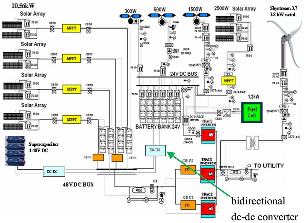
Figure 1. Schematic diagram of the distributed energy resources.
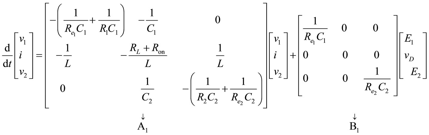
laboratory at University of Massachusetts Lowell (UML). A transformer less type was chosen so as to reduce size and weight, and improve economy [1]. Bidirectional power flow was obtained with a current-bidirectional two quadrant realization of the switch [2]. Anti-parallel-connected MOSFETs and diodes were used to construct the currentbidirectional switches. The power circuit includes the two control MOSFETs (APL 502J) 500 V, 52 A (switches Q1 and Q2); two diodes (APT2X101D20J) 200 V, 100 A (D1 and D2); inductor L and filtering capacitors C1 and C2.
The control circuit design and assembly is presented in Figures 3 and 4, and is composed of PIC16F684 microcontroller and FOD 3120 Optocoupler gate drivers, 2.5 A 8-DIP. A feedback loop system was used to control of the output voltage of the converter for a PWM. Reference 1 and Reference 2 on pins 12 and 13 of PIC 16F684 are connected through voltage divider from the 24 V and 48 V battery banks respectively, and they automatically control the pulse width that drives the MOSFET switches. Pin 9 and pin 10 of the PIC are connected to the sensors installed on load sides of the inverter.
3. The Operation
The current sensors, installed on the outputs of inverter 1 and inverter 2 (or 3), signals the micro-controller, and are responsible for determining the operation of DC-DC converter in either boost or buck mode. The micro-controller was programmed so that it could control the operation of the bidirectional DC-DC converter. The control strategies of this converter that are implemented in the PIC 16F684 are the following:
1) When the micro-controller reads that the current output in inverter 2 is higher than the current output in inverter 1, it will enable the PWM1. The microcontroller will drive MOSFET Q1 and operate as a buck converter.
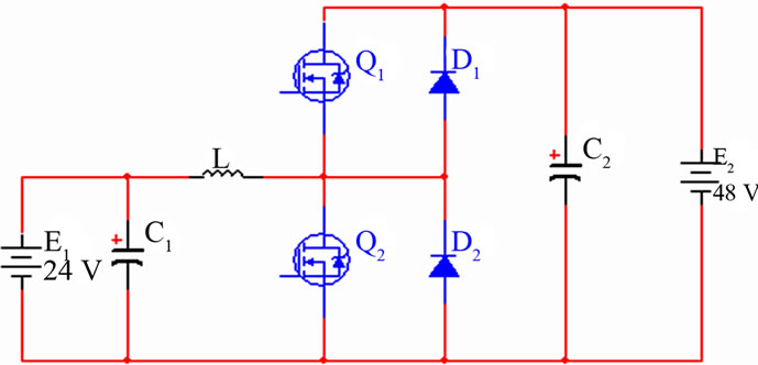
Figure 2. Power circuit of a bi-directional DC-DC converter.
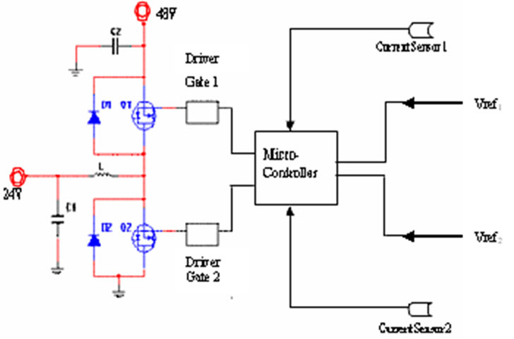
Figure 3. Control circuit block diagram for bidirectional DC-DC converter.
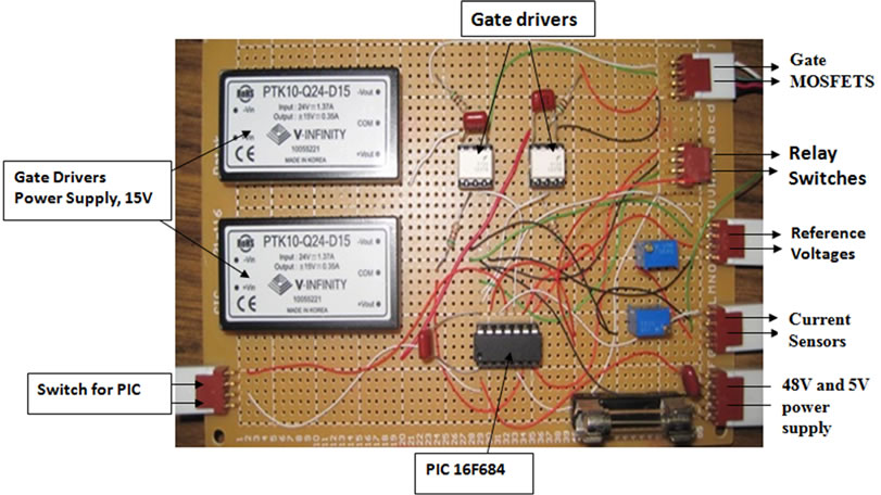
Figure 4. Control circuit assembly.
In this case, the 48 V battery bank supplies current to 24 V battery bank, and will supply current to inverter 1;
2) When the output current in inverter 2 is lower than the output current in inverter 1, it will enable the PWM2. The microcontroller will drive MOSFET Q2, so that the converter operates as a boost converter. In this case, the 24 V battery bank supplies current to 48 V battery bank, and will supply current to inverter 2;
3) If inverter 1 is not operational while the PV is connected and charging the 24 V battery bank, then the micro-controller will enable PWM2. The converter will operate as a boost converter. If inverter 2 is not operational while the PV connected to it is charging the 48 V battery bank, the micro-controller will enable PWM1. The converter will operate as a buck converter.
4. Steady State Analysis of the Bidirectional DC-DC Converter
The voltage and current equations of a DC-DC converter under steady-state conditions can be found by using the two basic principles namely; the principle of inductor voltsecond balance and the principle of capacitor amp-second or charge balance. The principle of inductor volt-second balance states that the average value, or dc component of voltage applied across an ideal inductor winding must be zero and the principle of capacitor amp-second or charge balance, states that the average current that flows through an ideal capacitor must be zero [3]. Thus, to determine the voltages and currents of DC-DC converters operating in periodic steady state, one averages the inductor current and capacitor voltage waveforms over one switching period, and equates the results to zero [4]. In Figure 5 the resistance RL of the inductor in the bidirectional DC-DC converter power circuit is being considered in order to model the circuit. Based on the power circuit shown in Figure 5, the output voltage, and inductor current were derived. Red arrows are in the direction of current in a step down mode while the black arrows indicate the current direction in a step up mode.
Boost Mode:
Figure 5 shows the equivalent circuit and the direction of currents and voltages when the DC-DC converter operates in the boost or buck mode. Each mode of operation consists of two intervals: the first is when the MOSFET is conducting and the second is when the appropriate diode is conducting.
Interval 1: When stepping up, MOSFET Q2 is on and MOSFET Q1 is off and inductor current flows through Q2 as shown in Figure 6.
Interval 2: When MOSFET Q2 is switched off at t = t1, the inductor is connected between the input and output voltages through diode D1 and the current that is flowing through MOSFET Q2 will now flow through L, D1, C2 and load R2 as shown in Figure 7. The output voltage and inductor current can be derived as:
At interval 1: When stepping up, the MOSFET Q2 is on and MOSFET Q1 is off, the inductor voltage is equal to;
 (1)
(1)
If the ripple is very small, i(t) can be approximated with its dc components IL, and thus,
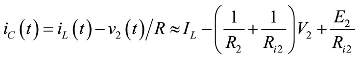
The output capacitor current is equal
which can be approximated as
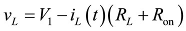
At interval 2: when MOSFET Q2 is switched off at t = t1, the inductor is connected between the input and output voltages through diode D1, the current that is flowing through MOSFET Q2 will now flow through L, D1, C2 and load R2. The inductor voltage can now be written as
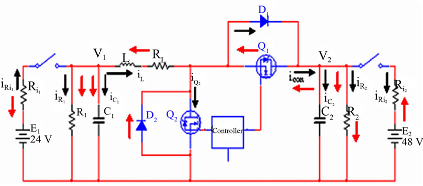
Figure 5. Voltages and currents for boost and buck DC-DC converter.
Figure 6. Interval 1: Currents and voltages for boost DCDC converter.
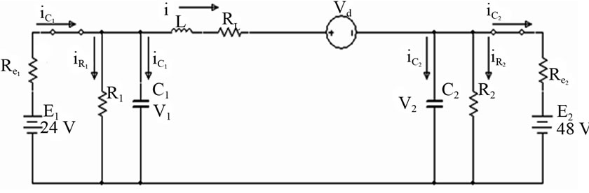
Figure 7. Interval 2: Currents and voltages for boost DCDC converter.
 (2)
(2)
The capacitor current can be expressed as
 (3)
(3)
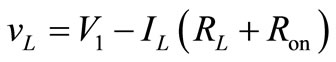
When the converter operates in steady state, the average value, or dc component of the inductor waveform vL(t) must be equal to zero and can be expressed as;
 (4)
(4)
Likewise, application of the principle of capacitor charge balance to the capacitor current waveform leads to
 (5)
(5)
Equations (4) and (5) can now be solved for the unknowns V2 and IL. The result is
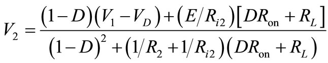 (6)
(6)
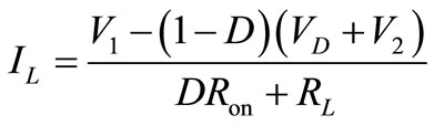 (7)
(7)
In order to charge the battery E2, the voltage across the capacitor V2 must be adjusted to be greater than voltage E2. Initially, the duty cycle D can be adjusted to make sure that V2 is greater than battery voltage E2 for boost operation. Based on Equation (7), it is expected that the charging current increases as the duty cycle increases. The resistance R2 must be greater than RL 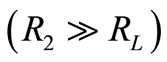 to make the converter operate most efficiently.
Buck Mode:
Figures 8 and 9 show the direction of currents and voltages when the converter operates in buck mode.
Interval 1: When stepping down, MOSFET Q1 is on and MOSFET Q2 is off, inductor current flows directly to the output as shown in Figure 8.
Interval 2: When MOSFET Q1 is switched off at t = t1, the current in the inductor that is flowing through MOSFET Q1 will now flow through diode D2 as shown in Figure 9.
The output voltage and inductor current can now be derived as;
 (8)
(8)
 (9)
(9)
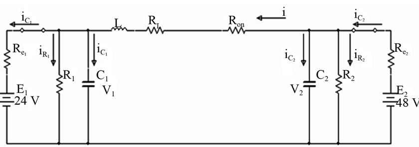
Figure 8. Interval 1: Voltage and current for buck DC-DC converter.
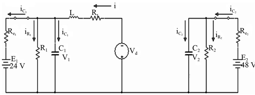
Figure 9. Interval 2: Voltages and currents for buck DC-DC converter.
In order to charge the battery E1, the voltage across the capacitor V1 must be greater than voltage E1. Again, the duty cycle D is initially set so that V1 is greater than battery voltage E1 for buck operation. The charging current can be adjusted by changing the duty cycle.
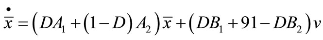
5. Dynamic Analysis of the Bidirectional DC-DC Converter
A typical configuration of a power circuit for a DC-DC converter, when considering voltage and current parameters, is shown in Figure 5. When the DC-DC converter operates as a boost or buck converter and in a continuous conduction mode, the current in the inductor flows continuously [5]. Red arrows are the direction of current in a step up mode while the black arrows indicate the current direction in a step-down operation. Based on this power circuit, the output and input voltages, and inductor current are being derived.
Boost Mode:
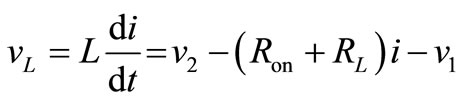
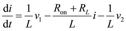
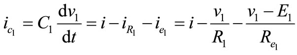
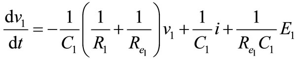
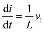
Interval 1: Switch Q2 is on, the inductor directly connected to source V1. Performing a Kirchhoff’s voltage law to the loop shown in Figure 6 gives;
 ;
; ;
; ;
;
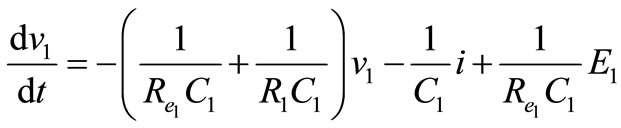 (10)
(10)
 (11)
(11)
and
 ;
; ;
; ;
;
 (12)
(12)
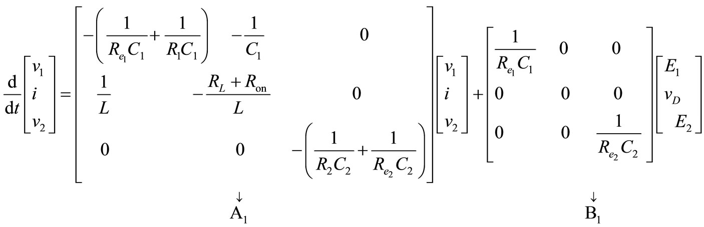
In matrix form, (see Equation (13))
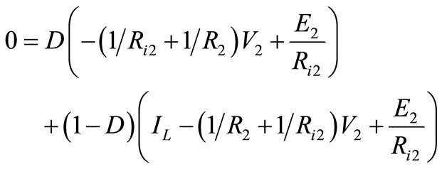
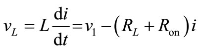
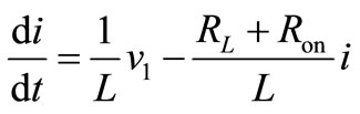
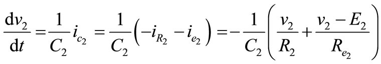
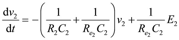
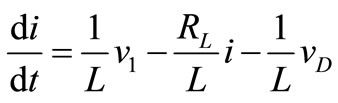
Interval 2: Switch Q2 is off, the V1 is directly connected to the output. The current that is flowing through Q2 will now flow through diode D1. Performing a Kirchhoff’s voltage law from input and to the output loop of Figure 7 gives;
 (14)
(14)
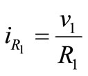
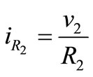
For vL, we have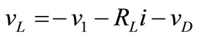 ;
; 
 (15)
(15)
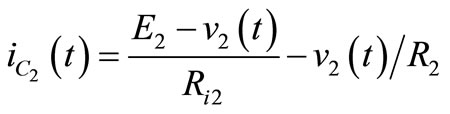
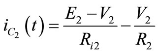
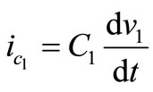
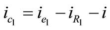
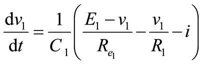
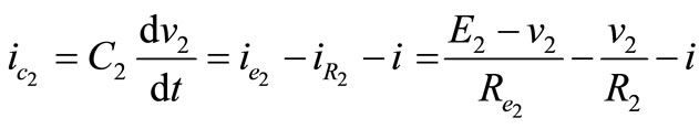
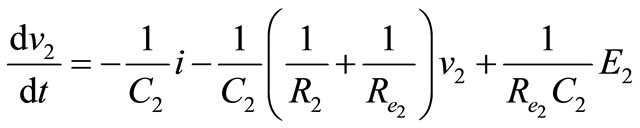
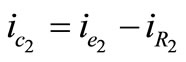
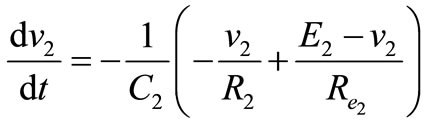
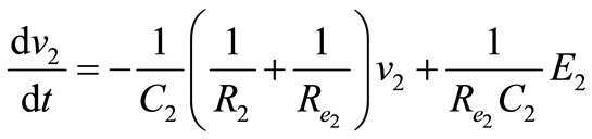
For ic we have; ;
;
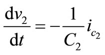 ;
; ;
; 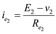
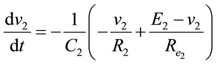
 (16)
(16)
In matrix form, (see Equation (17))
And let ,
, 
Then,
 (18)
(18)
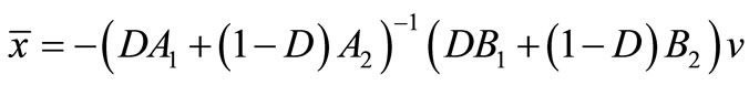
At steady state, 
 (19)
(19)
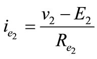
Buck Mode:
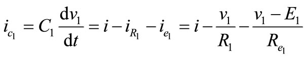
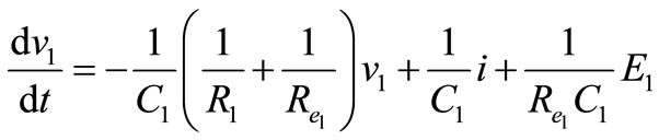
Interval 1: Switch Q1 is on, the V2 is directly connected to the output. Performing a Kirchhoff’s voltage law from input and to the output loop in Figure 8 gives;

 (20)
(20)
 (13)
(13)
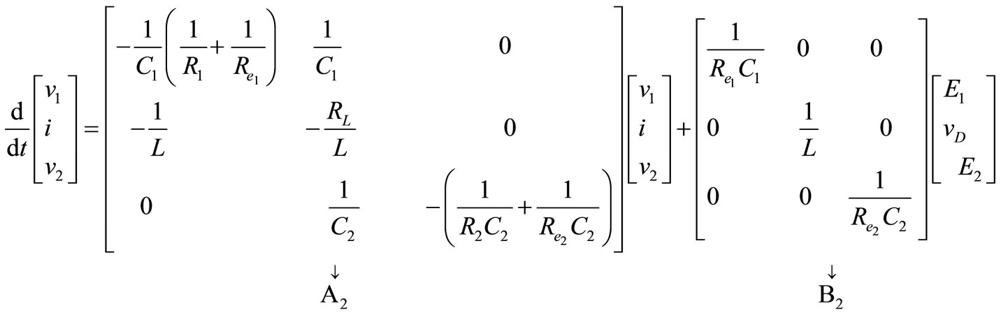 (17)
(17)
 (21)
(21)
 (22)
(22)
In matrix form, (see Equation (23))
Interval 2: Switch Q1 is off, the V2 is not connected to the output. The current that is flowing through Q1 will flow through diode D2. Performing a Kirchhoff’s voltage law from diode D2 and to the output loop in Figure 9 gives;
 (24)
(24)
For vL, we have
 ;
; 
 (25)
(25)
For ic we have;
 ;
; 
 ;
; 
 (26)
(26)
In matrix form, (see Equation (27))
And let ,
, 
Then,
 (28)
(28)
At steady state, 
 (29)
(29)
6. The Simulink Model
Based on the design of the power and control circuits presented in the previous section, an equivalent simulink model of the bidirectional DC-DC converter was constructed and is presented in Figure 10. In the simulink model, a PID controller is used to implement the control design for the system especially for generating a PWM that drives the MOSFETs and switch relays [9]. All the parameters are based on the actual component values used in the fabrication of the bidirectional DC-DC converter.
 (23)
(23)
 (27)
(27)
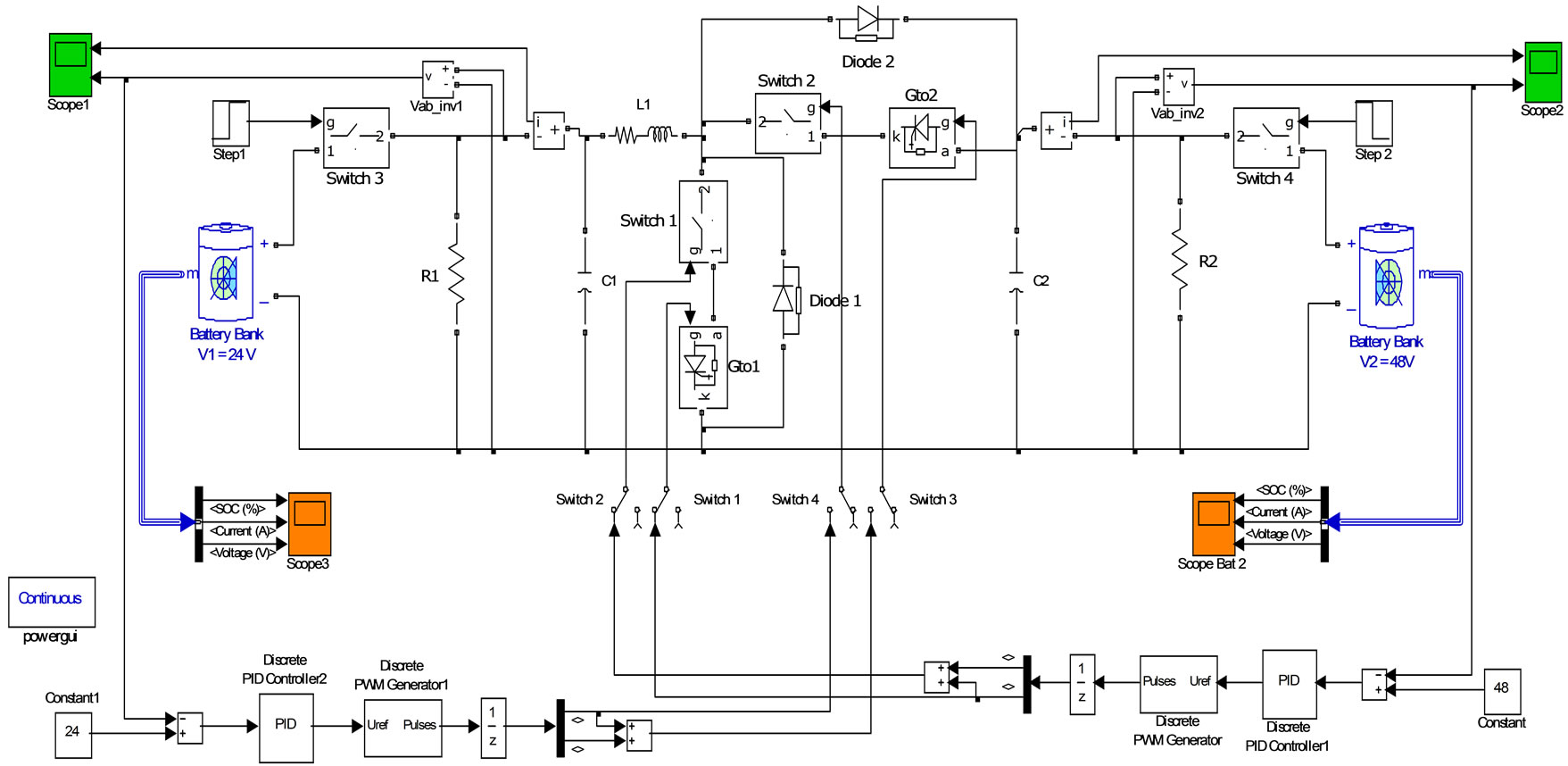
Figure 10. Simulink model of a DC-DC converter.
7. Simulation and Experimental Results
The system is simulated in order to examine the dynamic and steady state performance of the bidirectional DC-DC converter during buck and boost modes of operation [10]. Results of the voltage transient response for boost and buck operation of the bidirectional DC-DC converter are presented in Figures 11 and 12. In the simulation, the authors have used the actual values of the following parameters: Inductor (L) = 10 mH; Inductor resistance (RL) = 0.008 Ω; Capacitor 1 (C1) = 27,000 μF; Capacitor 2 (C2) = 27,000 μF; R1 = R2 = 750 Ω; and battery internal resistances Ri1 = 0.786 mΩ (for 24 V); Ri2 = 1.57 mΩ (for 48 V). Results show that the simulation is in good agreement with the experimental results, and validate the model.
It is also noticed that the response time is quite fast, taking only 0.25 sec to reach the steady state voltage V1 which is equals to 24.5893 volts for buck operation. While in boost operation, it also took 0.25 sec to reach the steady state voltage value V2 which is equals to 48.032 volts. While the current flowing to the inductor gives identical results for boost and buck operation but opposite in direction. It is found that the duty cycle for buck and boost operation must be greater than 50% in order to charge or transfer energy from one battery bank to another. And as the duty cycle increases, the current flowing through the inductor increases which will also increase the amount of energy transfer from one battery bank to another. It is observed that if the duty cycle is less than 50% for boost and buck operation, then the inductor current tends to be the opposite, meaning that it is not supplying or charging the output.
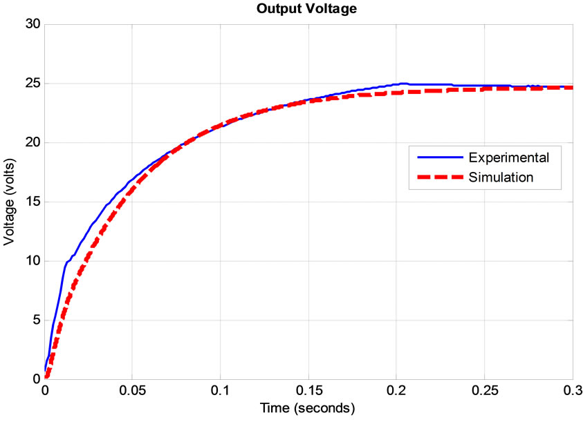
Figure 11. Voltage output transient response for buck operation.
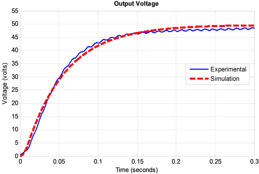
Figure12. Voltage output transient response for boost operation.
The actual installation was done with the low side of the converter connected to the 24 V battery bank and the high side connected to the 48 V battery bank as shown in Figure 13 while Figure 14 shows the variation of voltages and currents of the bidirectional DC-DC converter when it is operated experimentally. The system was tested on May 16, 2011 at 10:27 AM, on a cloudy day. When the circuit breakers on both side of the converter are switched on, the initial mode is in step up operation where average voltages and currents are: at low side; 23 V, 11.16 A, and high side; 49.6 V, –3.03 A. When the mode of operation changes to step down, the direction of current changes and the average low side and high side voltages and currents become 25.2 V, –10.83 A and 49.07 V, 7.04 A respectively. It is noticed that the voltage change on the high or low side of the converter conforms to the type of mode of operation but the efficiency in buck mode is greater than the efficiency in boost mode operation because the control circuit is connected to the 24 V battery source. It is also observed that the voltage and current change quickly without any overshoot of the values as the mode of operation changes. Hence, the converter’s voltage and current are stable as it operates in both directions.
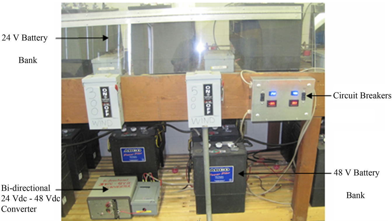
Figure 13. Actual operation of the bi-directional DC-DC converter.
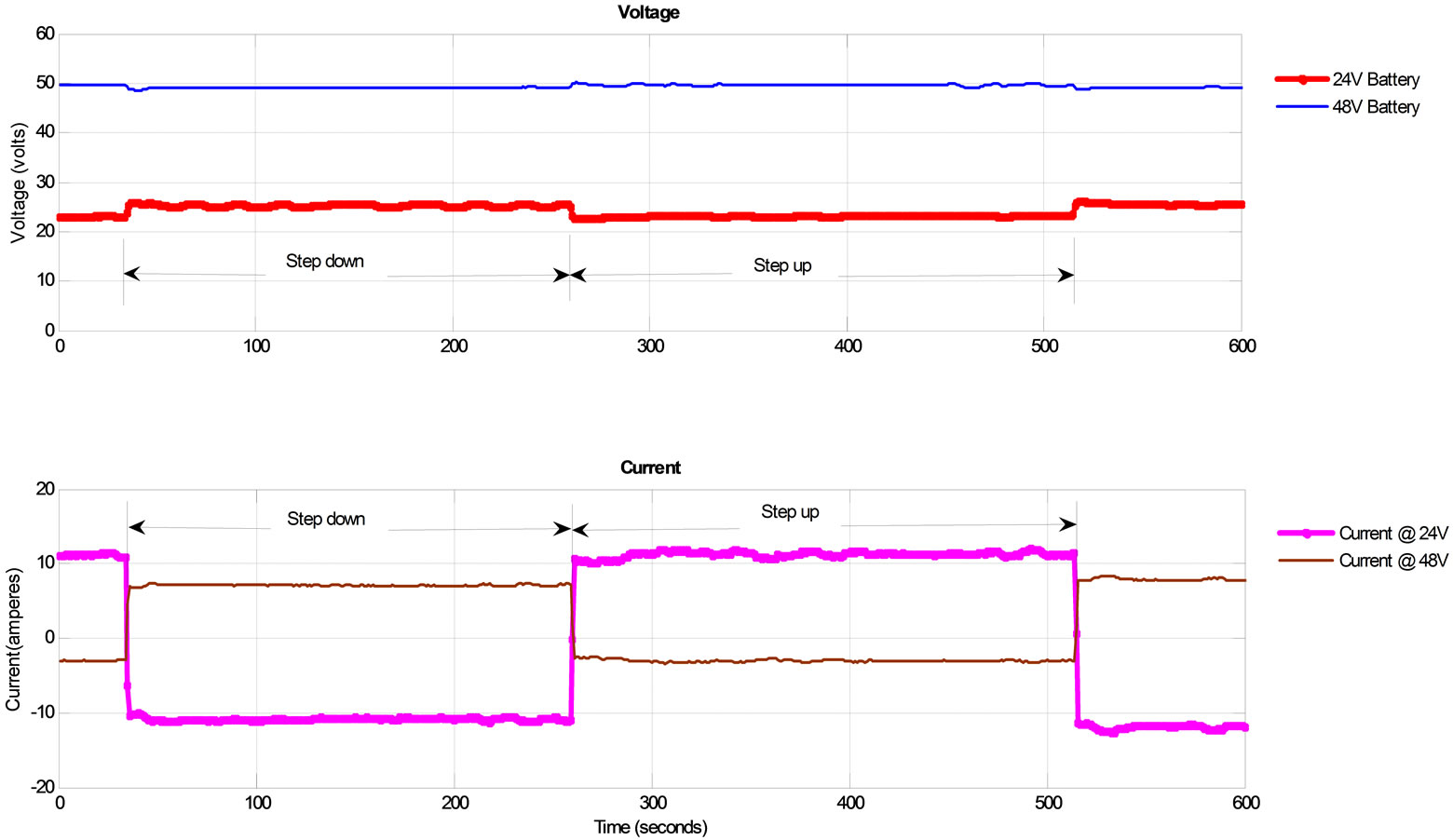
Figure 14. Voltage and current output of the bi-directional DC-DC converter.
8. Conclusion
A bidirectional DC-DC converter for distributed generation application has been designed, simulated and fabricated. Mathematical models for the buck and boost modes of the DC-DC converter are derived. Transient performances of the bidirectional DC-DC converter using the derived mathematical models are simulated in a Matlab Simulink environment. It is observed that the current change its direction quickly as the mode of operation changes without any overshoot of the values. Hence, the converter’s voltage and current are stable in its operation in both directions. Results show that the simulation is in good agreement with the physical experiment and they validate the model. The PIC16F684 micro controller successfully works well in the implementation of the designed control strategy design of the bidirectional DCDC converter. It was observed that the duty cycle for buck and boost operation must be greater than 50% in order to charge or transfer energy from one battery bank to another. And as the duty cycle increases, the current flowing through the inductor and load also increases with a corresponding increase in the amount of energy transfer from one battery bank to the other.
REFERENCES
- K. Hirachi, M. Yamanaka, K. Kajiyama and S. Isokane, “Circuit Configuration of Bidirectional DC/DC Converter Specific for Small Scale Load Leveling System,” IEEE Transactions on Power Conversion, Vol. 2, 2002, pp. 603-609.
- G. Y. Chang, W. C. Lee, K. C. Lee and H. C. Bo, “Transient Current Suppression Scheme for Bi-Directional DC-DC Converters in 42V Automotive Power Systems,” Journal of Power Electronics, Vol. 9, No. 4, 2009, pp. 517-525.
- S. Rahmani, K. Al-Haddad and H. Y. Kanaan, “Two PWM Techniques for Single-Phase Shunt Active Power Filters Employing a Direct Current Control Strategy,” IET Power Electron, Vol. 1, No. 3, 2008, pp. 376-385. doi:10.1049/iet-pel:20070253
- J. G. Lee, S. Y. Choe, J. W. Ahn and S. H. Baek, “Modelling and Simulation of a Polymer Electrolyte Membrane Fuel Cell System with a PWM DC/DC Converter for Stationary Applications,” IET Power Electron, Vol. 1, No. 3, 2008, pp. 305-317. doi:10.1049/iet-pel:20060413
- M. H. Rashid, “Power Electronics-Circuits, Devices and Applications,” 3rd Edition, Pearson Education, Upper Saddle River, 2003.
- J. P. Agrawal, “Power Electronics Systems Theory and Design,” Prentice-Hall, Inc., Upper Saddle River, 2011.
- A. Cultura and Z. Salameh, “Design and Installation of a 10.56kWp Grid-Tied PV Power System at University of Massachusetts Lowell,” POWER-Gen Renewables and Fuels Conference, Las Vegas, 6-8 March 2007.
- W. Na and B. Gou, “Analysis and Control of Bidirectional DC/DC Converter for PEM Fuel Cell Applications,” IEEE Power and Energy Society General Meeting—Conversion and Delivery of Electrical Energy in the 21st Century, Pittsburgh, 20-24 July 2008, pp. 1-7.
- http://www.mathworks.com/ products/simulink/
- http://www.fairchildsemi.com/