Energy and Power Engineering
Vol. 4 No. 4 (2012) , Article ID: 20213 , 8 pages DOI:10.4236/epe.2012.44025
H-Bridge Hybrid Converter Modeling and Synthesize with Power Sharing Analysis
School of Electrical Engineering, Iran University of Science & Technology, Tehran, Iran
Email: Aryan_770@yahoo.com, rahmati@iust.ac.ir
Received February 8, 2012; revised March 18, 2012; accepted March 28, 2012
Keywords: Hybrid Converter; None Ideal Modeling; Small Signal; Equilibrium Point; Power Sharing
ABSTRACT
In this paper hybrid converters with double inputs are investigated. Mainly any possible topologies are constructed and only one of them is chosen and modeled in none ideal format, by state space averaging method. After that small signal model and equilibrium point of that model is calculated. Finally with power sharing analysis the best point in efficiency was calculated.
1. Introduction
Hybrid power electronic dc-dc converters are useful in modern usages such as new energy sources like wind, solar power generation or fuel cells. Their most important feature is that, we can combine two energy sources with different voltages or power to achieve one voltage at output. Therefore if one of them is limited or not available the other can feed the load individually [1,2].
Multi input converters can be developed in different ways [3-9], but this paper focuses on a practical and systematic one. In this topology two H-bridge converters are cascaded to develop a new hybrid one. By combining H-bridge converters with other electrical devices like capacitors, inductors and diodes, finally four hybrid converters are derived, that is explained later. After that one of them is selected and is modeled in non ideal form by using state-space averaging method. Because hybrid H-bridge converters modeling is so similar to each other, so only one of them is modeled.
Furthermore transfer functions of the converter are extracted. After that efficiency equation is extracted and the best point in this equation is calculated. Finally with simulation the small-signal models and transfer function are verified too.
2. Hybrid Converters Introduction
2.1. Basic Topologies and Basic Elements Definition
Basic operation of any dc-dc converter is charging and discharging from one source of energy to other in specified period of time to achieve direct voltage without any ripple and changes. A big capacitor is also one important part that stores the energy which is consumed by the load. The other part is inductor that controls the rate of energy flow from one source to the other and it is controlled by switching elements which is independent from converter topology. In hybrid ones these switching elements furthermore combine two similar H-bridge converters that can charge or discharge inductor and feed the load together or individually. Therefore at any period of time, one, two or no voltage sources are connected to the circuit and output voltage is controlled in this period of times. Figure 1(a) is H-bridge cell, it contains four switches and one voltage source.
2.2. Combining Two Similar Cell
If two similar H-bridge converters are combined in series as shown in Figure 1(b), the basic part of hybrid converter is created. Three terminals can be connected in three models through inductor and capacitor to load as shown in Figure 2.
In topology of Figure 2(a), the output of first converter is named V1, and second one is named V2. By changing switch states, sixteen modes at the output can be achieved, four modes for the first H-bridge converter and four modes for the second. In these sixteen modes it is clear that some states are similar. After that at some modes the voltage that is generated in the output is negative, therefore in these states the energy is rolling back to the source and these modes are useful in bidirectional converter and discharging inductor too. Therefore we can simplify this table into Table 1 that similar states are removed and just one negative voltage that requires
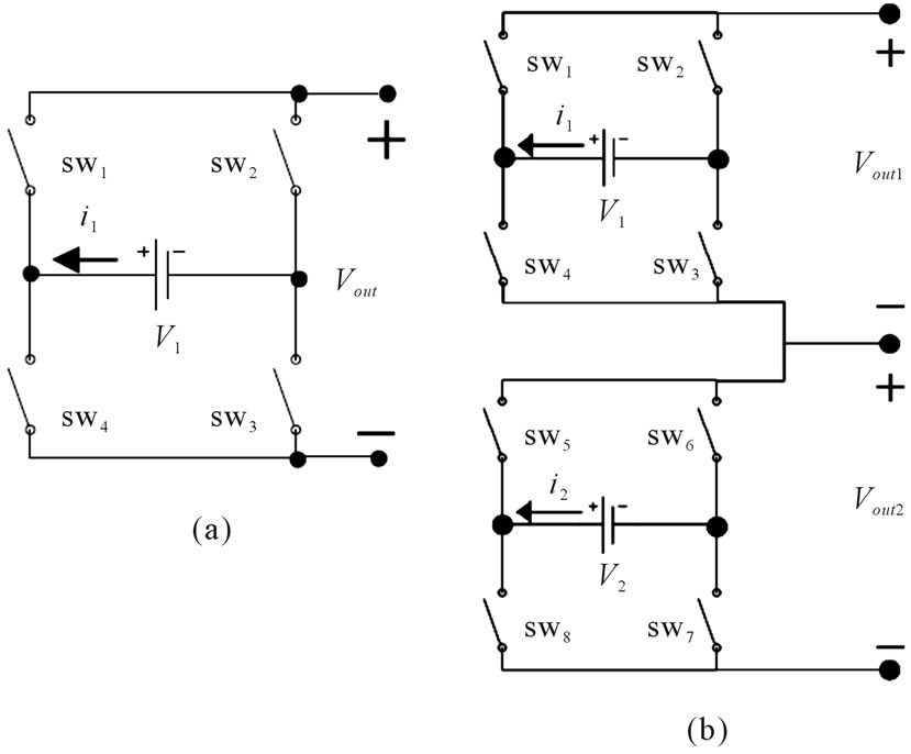
Figure 1. H-bridge cell. (a) Single H-bridge cell; (b) Hybrid H-bridge.
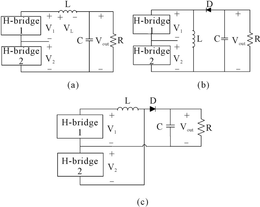
Figure 2. Three topologies for hybrid H-bridge converter.

Table 1. Simplified modes of first converter.
discharging the inductor is left. It is necessary to have at least one negative state for discharging otherwise inductor will be rolling slowly to saturation condition.
In Table 1 switch states are shown. Some of them are shorted in all periods of time so we can replace these switches by short-circuit instead. Therefore sw3 and sw7 are shorted in all periods of time. After that sw4 and sw8 are opened in four states and could be removed for simplifying the circuit. Among the other switches only sw1, sw5 are left as switches because their state is changed between ON and off according to time period. These switches must block voltage and current so they are switches and they can be replaced by IGBT. sw2 and sw6 are not independent switches and they work in inverse states of sw1 and sw5, but because of simplifying the circuit of converter and switching signal generation they can be replace by diodes. Because diodes block negative current.
Now the basic topology illustrated in Figure 2(a) is converted to Figure 4(a) in which switches are replaced by suitable components. If we synthesis the other two topologies shown in Figure 2 the other converters are created, like Figures 4(b)-(d).
In all four hybrid converters it is possible to indicate basic dc-dc converter topologies: buck, boost and buckboost. For example Figure 4(a) is created by combining two buck converters and it can be named buck-buck converters which is chosen to describe and modeled entirely in this paper. This type of naming is because of better classification of hybrid converters, on the other hand it can be shown that hybrid converters can increase or decrease voltage from sources to output or even they can decrease one source and increase the other in specific usage and for special input sources.
3. State-Space Averaging Principles and Small Signal Modeling
In this part converter modeling is described. State-space averaging is used and the equations are calculated based on converter circuit shown in Figure 3. State space averaging is a powerful method of both calculating the steady state values of voltages and currents and extracting the small-signal model of switching converters .In this method at beginning, the state equitations are written in every time periods then every states are multiplied in Owen time durations. Then by averaging between these equations the final model is produced. At last by separating the static and dynamic parts the dynamic model and the steady values are calculated.
Converter circuits are modeled in non ideal form therefore equations could be used in practical experiments which are validated by simulation at the end.
3.1. Switching Time Periods
Before modeling it is necessary to describe the switching time period. In fact because of combination, the switching time period is very important at the output voltage changes. The basic time period pattern is shown in Figure 4.
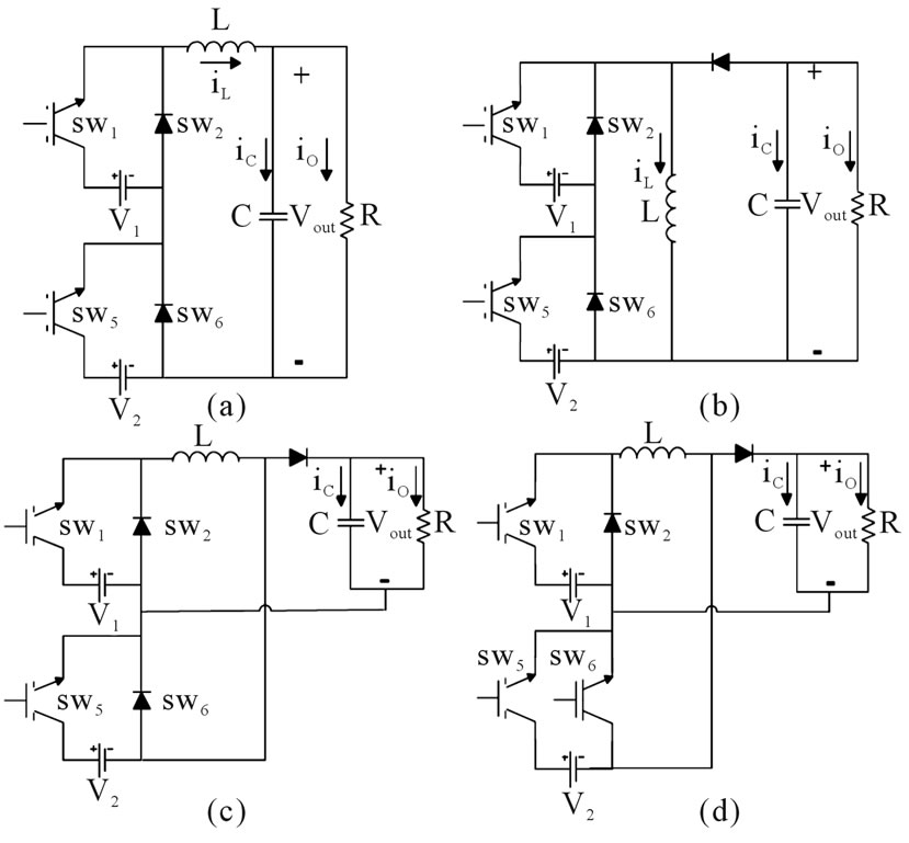
Figure 3. Four simplified hybrid H-bridge converter.
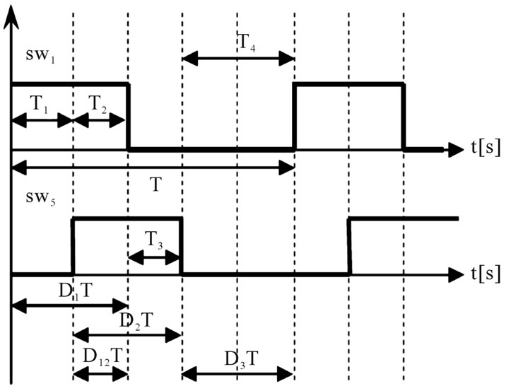
Figure 4. Switching timing of hybrid converter.
In this figure T is switching period. In Figure 4, D1T is the time in which sw1 is ON therefore V1 feeds the load in this period of time. D2T is sw5 ON state time. It means that in this period of time sw5 is ON and current can flow throw it. Because there is an overlap between D1 and D2 there is a period of time in which two converters feed load and it is named D12. Because of discharging requirement it is necessary that, there is a period of time in during, both of converters are left OFF and it is named D3. These timings are rewritten in Equation (1):
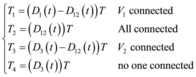 (1)
(1)
After describing duty cycles now the converters can be modeled by state-space averaging method. Using this method furthermore it is possible to calculate small-signal model and equilibrium point too [10,11].
3.2. State Equations Calculation and Modeling Equations Extraction
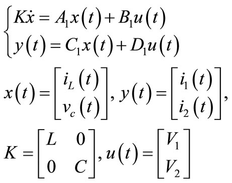
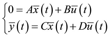
In this method at beginning the state equations are written in every time periods and at last, by averaging the final model is produced. Equation (2) shows state equation in standard form.
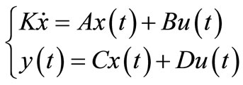 (2)
(2)
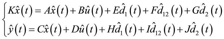
In this equation x(t) is state variable matrix, u(t) indicates inputs and it is a 2 × 2 matrix. K is a diagonal matrix that contains capacitor and inductor values. y(t) is chosen as the output variable and it can be any variable in the circuit.
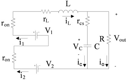
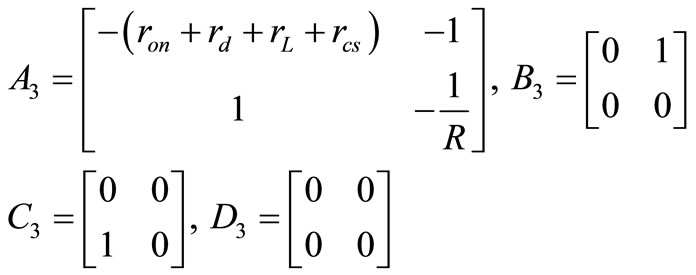
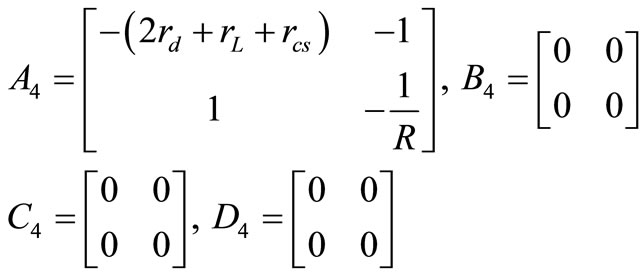
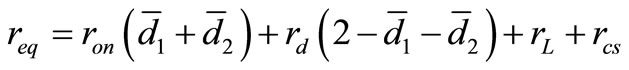
A is characteristic matrix that shows converter properties. Finally B, C and D connect input matrix and state variables matrix together. Figure 5 shows subintervals of converter during four time periods. During T1, switch sw1 is ON and sw2 is OFF. Therefore only v1 is connected to the load. Because of non ideality in modeling, parameters ron, rd, rl and rcs are added. In this figure resistor, ron is switch resistant that makes main losses on switches. rd is the resistance of diode and it can be selected so that it can model diode voltage drop too. In fact we can assume that because of rd, there is a voltage drop across the diode. Furthermore rl is the inductor resistance. Finally for capacitor parasitic effects modeling, it is useful to specify two resistances. One of them is rcs, that is in series with the capacitor and it is used for non ideal processing in technology. rcp, is the parallel one which is paralleled with the load resistor too, this resistance can be merged with the load resistance.
During T1, as shown in Figure 5(a) circuit equations are indicated in Equation (3):
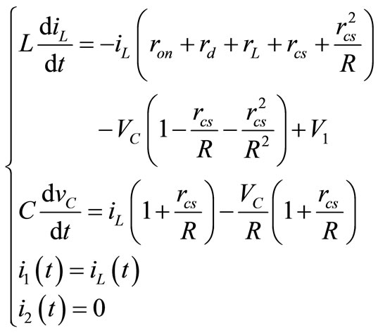 (3)
(3)
In these equations state variables are iL and vC and they are written in term of other variables. Therefore we can summaries Equation (2) in state equation form like Equation (2). We select 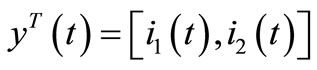 because they are so useful in calculating input power and furthermore efficiency equations.
 (a)
(a)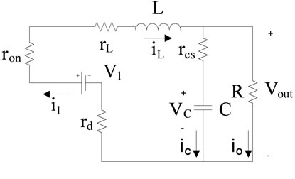 (b)
(b)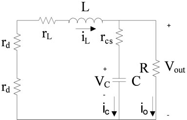 (c)
(c)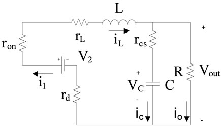 (d)
(d)
Figure 5. Buck-buck converter subintervals.
 (4)
(4)
In Equation (3) because  therfore it is possible to remove terms
 . After simplification, the equation is written in state equation form then it is possible to extract A, B, C and D matrixes, for first time duration according to Equation (3), Equation (5) is extracted in form of matrixes:
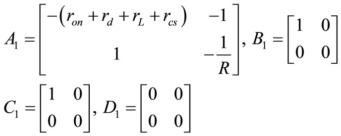 (5)
(5)
By doing this calculation for the other three remaining subintervals the three groups of four matrixes are extracted too.
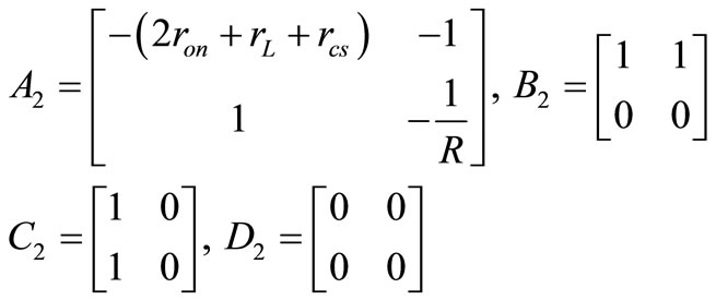 (6)
(6)
 (7)
(7)
 (8)
(8)
Now every set of equations must be multiplied by own time duration and after that they must be summed with each other and then the average is calculated so the result is:
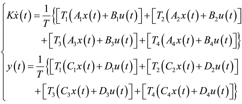 (9)
(9)
The above equation consists of equilibrium points and small signal terms. Therefore they must be separated from each other. It is possible to assume:
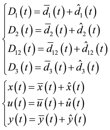 (10)
(10)
In Equation (10) the ^ sign is specialized for changes and separates small signal values from constant values which is indicated by bar sign on them.
After substituting these parameters in Equation (9) and categorizing similar values, separation is possible between small signals and equilibrium point’s equation:
Equilibrium equations are:
 (11)
(11)
In which A is calculated by combining Ai’s, i = 1, 2, 3 and 4. B, C and D matrixes are also derived in this way therefore these matrixes are extracted:
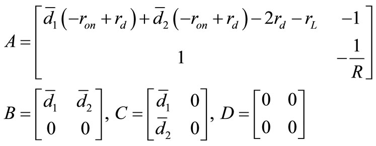 (12)
(12)
Now it is possible to calculate first term of Equation (11) and equilibrium point produced by:
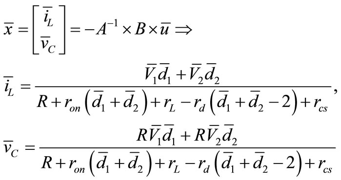 (13)
(13)
And for output parameters by calculating second term of Equation (11) then 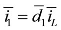 and
and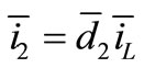 .
.
For small signal analysis If we group terms with ^ sign substituted in Equation (9) then this equation will be produced:
 (14)
(14)
where A, B, C and D are calculated above and E, F, G, H, I and J matrixes could be calculated in similar way, they will be:
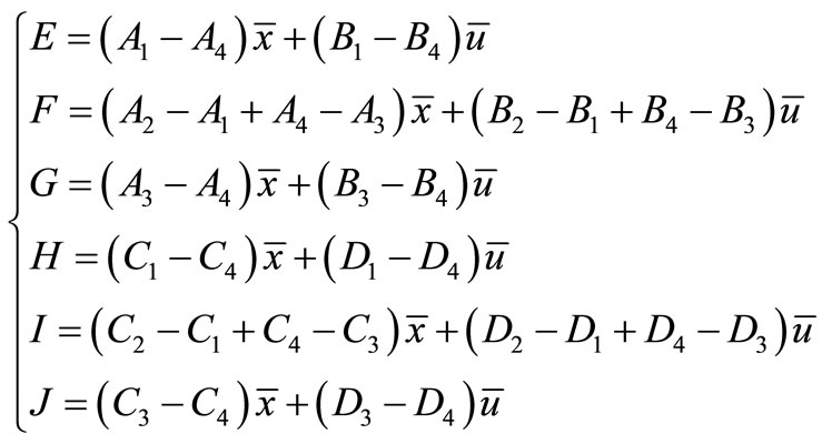 (15)
(15)
Therefore:
 (16)
(16)
For this converter if this calculation is done for other three hybrid converters shown in Figure 4 they have different matrixes but the algorithm is like this sample.
For small signal modeling extraction, Equation (11) is used. If it is expanded in scalar format it is found out that every change in inductor and capacitor voltage as state variables is because of changing in other circuit parameters. Therefore it is useful to investigate this state variable in the presence of only one of these changes and finally with superposition this state variable can be linked to all parameters too. After expansion Equation (11) will be:
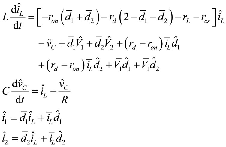 (17)
(17)
In Equation (17) every term shows only one change. Now for better understanding it is so amazing to convert above terms into a circuit that can model the converter without mathematical operation and only by electrical devices. For this purpose it is possible to draw a circuit for every four group of equations in Equation (14). Figure 6 shows this four group circuit.
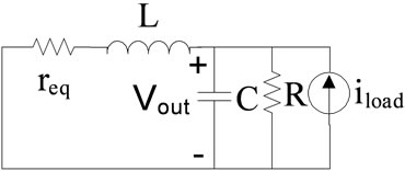
Furthermore they could be combined to produce a compact circuit which is more useful for modeling, Figure 7 shows this circuit. In this circuit  is representing load changes and could be modeled in current supply shape.
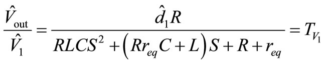
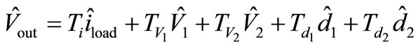
4. Transfer Function Extraction
Till now the electrical converter model is extracted but for controller design [12], efficiency or output dynamic response it is better that transfer function is calculated too. For this purpose the circuit shown in Figure 7 is useful but the problem here is that there are at least five sets of input in circuit. They are ,
,  ,
,  ,
,  and
and . They are named input because they can change the output. Now according to superposition it is possible to separate the inputs and for each one ,one transfer function is extracted, for this reason at first
 ,
,  ,
,  ,
,  is set to zero and circuit simplifies as shown in Figure 8(a).
 (a)
(a)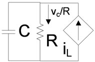 (b)
(b)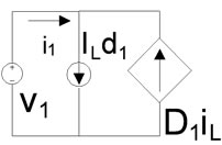 (c)
(c)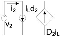 (d)
(d)
Figure 6. The circuit which extracted from equations.
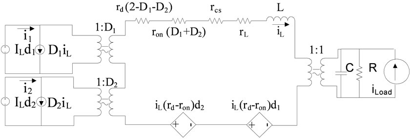
Figure 7. Combined circuit.
 (a)
(a)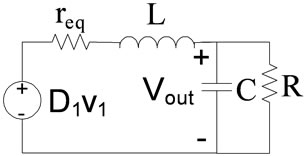 (b)
(b)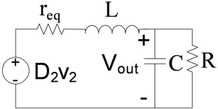 (c)
(c)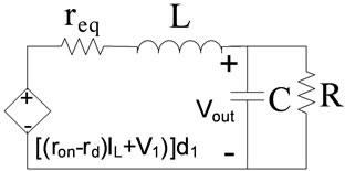 (d)
(d)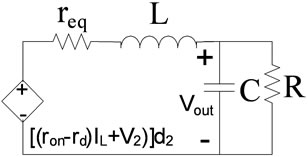 (e)
(e)
Figure 8. Circuit for transfer function extraction.
In this circuit the transfer function could be extracted:
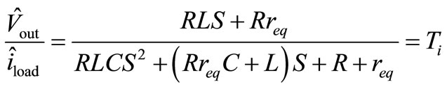 (18)
(18)
In this equation
which is produced because of non ideality of devices in model. This term is present in all transfer functions. If ,
,  ,
,  ,
,  are set to zero something like Figure 9 appears. The transfer function will be:
 (19)
(19)
And as like above for Figure 8(c) the transfer function will be:
 (20)
(20)
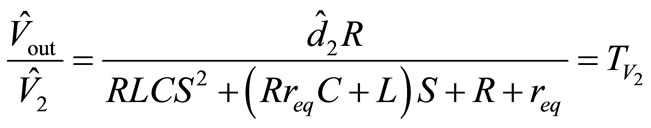
And finally two other remaining transfer functions according to Figure 6(d) are:
 (21)
(21)
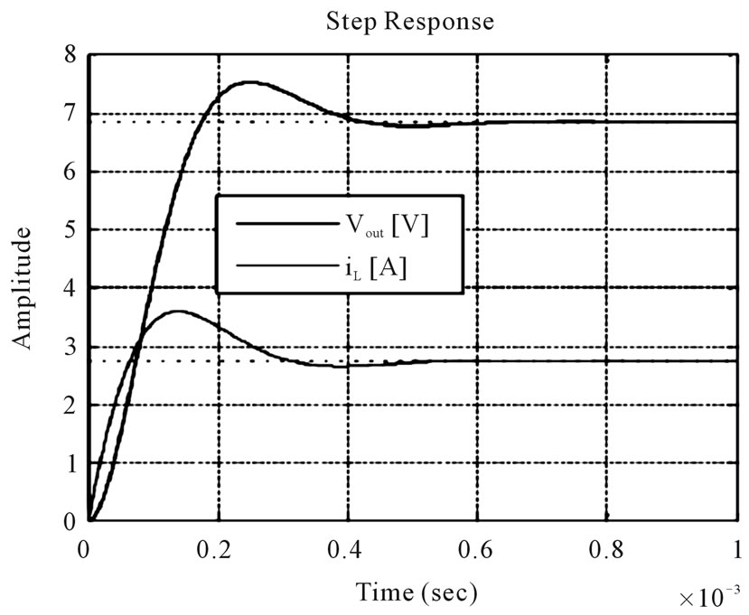
Figure 9. Transfer function response.
Ti shows the changing in load how much can change the output.  And
And  are the most important transfer functions because they are main transfer functions and show the effect of input power supplies on output voltage.
  And
And  show the effect of changing in duty cycle on output voltages. Perhaps it is useful to rewrite the equation in term of transfer functions:
 (22)
(22)
If this method is done for the other state variable, iL, its transfer function is calculated too. For example two important ones are:
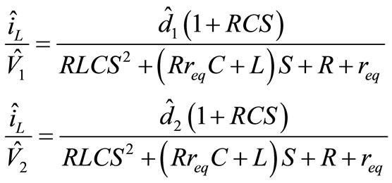 (23)
(23)
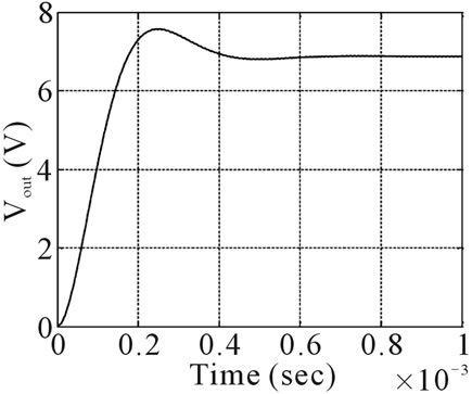
5. Small Signal Models Verification and Simulation Result
In this part models that were constructed before are compared with simulation results. Simulations are in MATLAB-SIMULINK. Figure 9 shows the response of transfer functions and Figure 10 shows simulation result. As we see they are similar in steady state and even in transient. For simulation we use step changes in V1 and V2 independently and state variable which consists of iL and vC is calculated in front of changes in input voltage sources. For simulation we choose these values for components:
 (a)
(a) (b)
(b)
Figure 10. Simulation results (a) Output voltage; (b) Inductor current.
For inductor and capacitor calculation we use Equations (24)-(26) which can calculate a typical value for these components. Parasitic resistant is chosen by some existing typical examples.
 (24)
(24)
 (25)
(25)
 (26)
(26)
6. Power Sharing Analysis
In this part at first, converter efficiency is calculated in non ideal form. After that ,any possible duty cycle which results in a constant output voltage is calculated and in every one, efficiency is extracted, therefore the best point that converter works in, is the point with maximum efficiency and less power dissipation.
6.1. Efficiency Calculation
Because modeling is based on non ideal devices it is possible to calculate losses of parasitic components. First the output power is calculated. It is useful to calculate it by equation below:
 (27)
(27)
After that the input power is calculated by equation below:
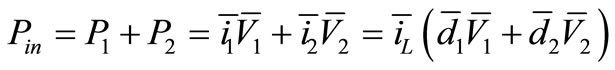 (28)
(28)
And we know from Equation (13) that inductor current calculated in term of  is:
is:
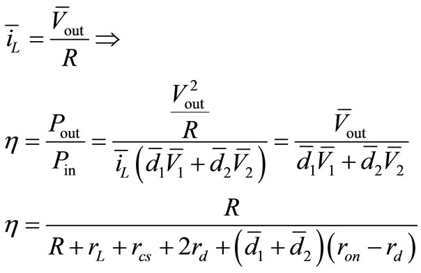 (29)
(29)
By changing  and
and  we can change efficiency, it is also possible by changing
  and
and . For example if we assume
  then only R,
  ,
,  and
and  can change efficiency and others have no effect on it.
6.2. Duty Cycles Extraction
By using Equation (13), if output voltage is kept at a constant value a group of D1 and D2’s are extracted. This calculation is done with V1 = 12 v, and V2 = 24 v and so Vout = 10 v. The result is illustrated in Figure 11. In this figure x-axis represents D1 and y-axis represents D2. It is clear that there are so many D1 and D2’s in which output voltage is 10 v. In Figure 11 this points are bolded. Finally in Figure 12 any possible efficiencies are illustrated and for desired output voltage the adjective points are bolded too. The buck-buck converter D12, is not effective in output voltage calculation and it is clear from Equation (13), therefore D12 is not involved in this part and for this converter. But for the other formats it might be involved in equations. Table 2 shows some of the result and the best point is bolded there.
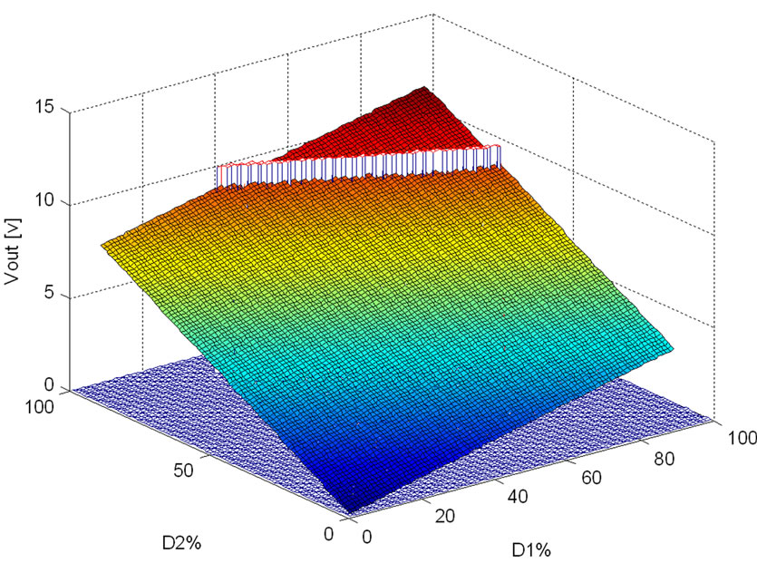
Figure 11. Possible output voltages in front of duty cycle changes.
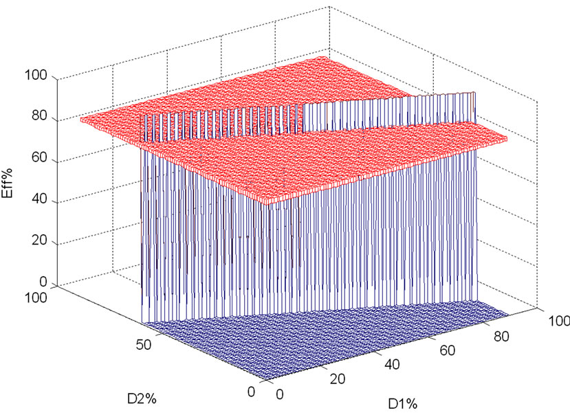
Figure 12. Possible efficiencies in front of duty cycle changes.
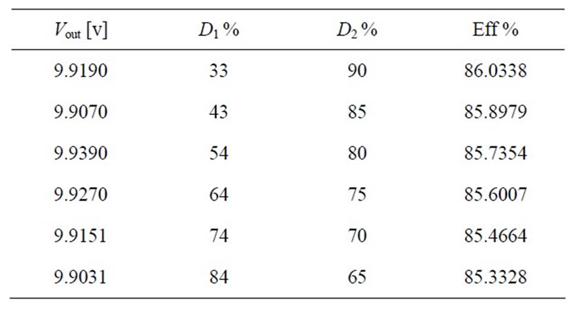
Table 2. Best efficiency point calculation.
7. Conclusion
In this paper some topologies for hybrid converters based on H-bridge were discussed. After that by choosing one of these converters, by non ideal modeling the effect of parasitic resistors like diode, switches, inductor and capacitor was investigated and equilibrium point and transfer functions of state variables were calculated. Finally by simulation, the results were validated and so the efficiency and output dynamic response and load current ripple were calculated for buck-buck converters. Furthermore power sharing was investigated and the best point to minimize energy dissipation was calculated.
REFERENCES
- Y. Levron and D. Shmilovitz, “Optimal Power Management in Fueled Systems with Finite Storage Capacity,” IEEE Transactions on Circuits and Systems—I: Regular Papers, Vol. 57, No. 8, 2010, pp. 2221-2231. doi:10.1109/TCSI.2009.2037405
- N. D. Benavides and P. L. Chapman, “Power Budgeting of a Multiple-Input Buck-Boost Converter,” IEEE Transactions on Power Electronics, Vol. 20, No. 6, 2005, pp. 1303-1309. doi:10.1109/TPEL.2005.857531
- K. Gummi and M. Ferdowsi, “Synthesis of Double-Input Dc-Dc Converters Using a Single-Pole Triple-Throw Switch as a Building Block,” Proceedings of PESC’08, Rhodes, 15-19 June 2008, pp. 2819-2823.
- H. Li, Z. Du, K. Wang, L. M. Tolbert and D. Liu, “A Hybrid Energy System Using Cascaded H-Bridge Converter,” Proceedings of Industry Applications Conference’07, Kosice, Vol. 1, 7-8 October 2006, pp. 198-203.
- Y. Li, D. Yang and X. Ruan, “A Systematic Method for Generating Multiple-Input Dc/Dc Converters,” Proceedings of VPPC’08, Harbin, 3-5 September 2008, pp. 1-6.
- Y. Li, X. Ruan, D. Yang, F. Liu and C. K. Tse, “Synthesis of Multiple-Input Dc/Dc Converters,” IEEE Transactions on Power Electronics, Vol. 25, No. 9, 2010, pp. 2372- 2385. doi:10.1109/TPEL.2010.2047273
- K. Kobayashi, H. Matsuo and Y. Sekine, “Novel Solar-Cell Power Supply System Using a Multiple-Input Dc-Dc Converter,” IEEE Transactions on Industrial Electronics, Vol. 53, No. 1, 2006, pp. 281-286. doi:10.1109/TIE.2005.862250
- Y. M. Chen, Y. C. Liu, F. Y. Wu and Y. E. Wu, “Multi-Input Converter with Power Factor Correction and Maximum Power Point Tracking Features,” Proceedings of APEC’02, Vol. 1, 2002, pp. 490-496.
- K. P. Yalamanchili and M. Ferdowsi, “Review of Multiple Input Dc-Dc Converters for Electric and Hybrid Vehicles,” Proceedings of VPPC’05, Chicago, 7-9 September 2005, pp. 160-163.
- A. Davoudi and J. Jatskevich, “Realization of Parasitic in State-Space Average-Value Modeling of pwm Dc-Dc Converters,” IEEE Transactions on Power Electronics, Vol. 21, No. 4, 2006, pp. 1142-1147. doi:10.1109/TPEL.2006.879048
- S. C. Wong, C. K. Tse, M. Orabi and T. Ninomiya, “The Method of Double Averaging: An Approach for Modeling Power Factor—Correction Switching Converters,” IEEE Transactions on Circuits and Systems—I: Regular Papers, Vol. 53, No. 2, 2006, pp. 454-462.
- B. Bryant and M. K. Kazimierczuk, “Open-Loop Power- Stage Transfer Functions Relevant to Current-Mode Control of Boost pwm Converter Operating in ccm,” IEEE Transactions on Circuits and Systems—I: Regular Papers, Vol. 52, No. 10, 2005, pp. 2158-2164. doi:10.1109/TCSI.2005.852919