World Journal of Nano Science and Engineering
Vol.04 No.03(2014), Article ID:49518,5 pages
10.4236/wjnse.2014.43014
The Effect of Carbon Rod―Specimens Distance on the Structural and Electrical Properties of Carbon Nanotube
Mohammad M. Uonis, Bassam M. Mustafa, Anwar M. Ezzat
Department of Physics, College of Science, Mosul University, Mosul, Iraq
Email: Bassam_alemam@yahoo.com
Copyright © 2014 by authors and Scientific Research Publishing Inc.
This work is licensed under the Creative Commons Attribution International License (CC BY).
http://creativecommons.org/licenses/by/4.0/


Received 29 June 2014; revised 28 July 2014; accepted 27 August 2014
ABSTRACT
The research studies the effect of the distance between the sample and the plasma sputtering source on the properties of the junction (silicon wafer-carbon nanotubes). The silicon wafer is fixed at (near, medium and far distances from the plasma source which is in the form of high purity graphite rod heated electrically). For the three cases, thickness of the sample is constant (20 nm). The samples were studied by scanning electron (SEM) and atomic force microscopes (AFM), X-ray and Raman spectra. For optimum distances the carbon layer is in the form of multi wall carbon nanotube (MWCNT). SEM images shows no formation of CNT on the Si wafer for near distance, which is consistent with the AFM images, X-ray and Raman spectrograms and no existence of characteristics (002) peaks whereas it appears for medium and longer distances, and by experience the optimum distance was found. This means that at closer distance high energy and high intensity plasma particles prevent the formation of CNT. This effect decreases with increasing distance of substrate from the graphite rod.
Keywords:
Carbon Nanotubes, Si-CNT Junction, Plasma Sputtering of CNT

1. Introduction
There are many applications of carbon nanotubes in various scientific fields such as electronics, materials, medical science and others. Researchers were interested in finding different methods to produce these nanotubes and to study different variables affecting these methods to gain best properties for these tubes: their directions of growth, lengths and densities. Different methods are used in the production of CNTS some of them involve very high temperature (arc discharge: 5000˚C - 20,000˚C, laser vaporization: 4000˚C - 5000˚C) and others are performed at low temperatures (chemical vapor deposition CVD: below 1000˚C) [1] .
In this work preparation of Si-CNT junction without catalyst was done using plasma-sputtering system. The effects of distance variation between the carbon rod and the samples on nanotubes productions and their optical properties have to be examined through the SEM & AFM images, X-ray and Raman spectra.
2. Experimental Method
Our research involves the production of Si-C junctions using plasma-sputtering method. The main procedure is through the conventional sputter chamber which is evacuated with a rotary pump until the vacuum level (10−2 tor), then Introducing Argon gas into the chamber to allow the vacuum to recover then. Apply the lowest voltage that will allow a plasma to strike the carbon rod [2] .
The carbon layers (20 nm thickness) were directly deposited on silicon wafer from carbon rods without any kind of catalysts [3] . The current flow through carbon rods is about 70 A. The effect of distance variation between the carbon rod and the samples on nanotubes productions and their properties was examined through the SEM, AFM images, X-ray and Raman spectroscopy.
The system for synthesis of carbon nanotubes on silicon wafers without catalyst by plasma sputtering method is shown in Figure 1. A high voltage is applied to the electrode causes an ionization of the gases, resulting in plasma formation. This method allows the control of growth parameters and as a result affecting the growth rate.
The most two important parameters in this technique are distance of the sample from the carbon rod thickness and the current flow through the carbon rod.
Measurements of the properties of the samples prepared by the above method are:
The surface microstructure obtained by a cold field scanning electron microscope (SEM) (JEUM-JSM-6756 F) operating at a voltage of 10 keV. Raman spectra measurements using spectrometer (GM SER No 87120) (Germany) which consists of a laser excitation beam that is focused through a microscope on the sample surface. The back scattered light intensity is measured as a function of its frequency shift. These shifts induced by the inelastic energy exchange between photons and vibration modes. The spectra obtained give information on the bonding environment in the sample. X-ray diffraction is done using the diffractometer (XRD, Bruker/D8-a with Cu Kα radiation λ = 1.54178 Å). The current-voltage characteristics obtained using the circuit shown in Figure 2 revealed a standard pattern as shown later.
3. Results & Discussion
Figure 3 shows scanning electron microscope images for 20 nm carbon layer deposited on silicon wafers. These samples were located at three different distance from carbon rod with 3 mm increment. For the three cases,
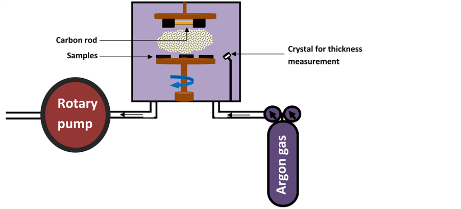
Figure 1. Schematic of plasma sputtering system.
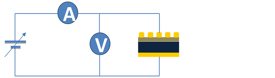
Figure 2. The circuit used for measuring I-V characteristics.

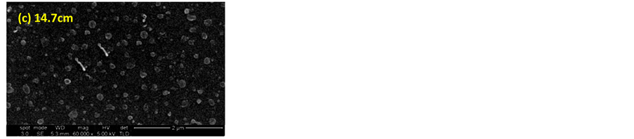
Figure 3. Scanning electron microscope images for the samples at three distance (a) 14.1 cm, (b) 14.4 cm and (c) 14.7 cm.
thickness of the sample is constant (20 nm) .the samples were studied by scanning electron (SEM) and atomic force microscopes (AFM), X-ray and Raman spectra. For optimum distances the carbon layer is in the form of multi wall carbon nanotube (MWCNT).
Figure 3(a) show the SEM image of the nearest sample to carbon rod (1.41 cm), SEM images shows no formation of CNT on the Si wafer for near distance, this is consistent with the AFM images, X-ray and Raman spectrograms where no existence of characteristics (002) peaks are noticed whereas Figure 3(b) & Figure 3(c) for the medium and longer distances shows formation of CNT. This means that at closer distance high energy and high intensity plasma particles prevent the formation of CNT, this effect decreased with increasing distance of substrate-graphite rod [4] -[6] .
Raman spectra for the samples revealed: the G and D bands appear for the smallest distances at 1610 - 1620 cm−1 and at 1360 - 1370 cm−1 respectively, also intensity of Raman peaks increase with distance by comparing (b) and (c) in Figure 4, while for the smallest distance (a) in the same figure, the peaks (D & G) disappeared [6] - [10] . The most noticeable features seen in Figure 4 are the increase in disorder induced D mode with distance increase, which ascribed to prevent the formation of the both phases (order and disorder modes) in the deposited carbon layers.
X-ray diffractogram shows the characteristic peak (002) of the graphite layers which indicate surly the existence of multiwall Carbon nanotube, intensity of the peak for smaller distance is lower than that of high distance [11] . From Figure 5, we can observe that some peaks, which belong to SiC, and disappeared with decreasing distance. This is fully compatible with the SEM images and Raman spectrum.
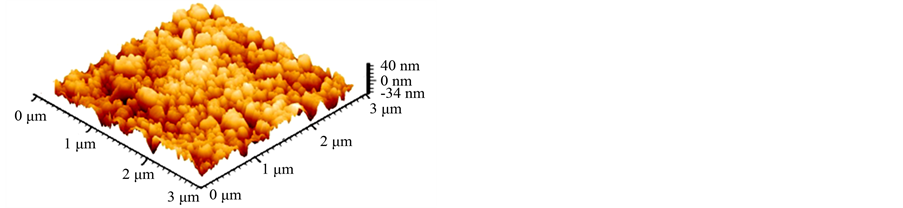
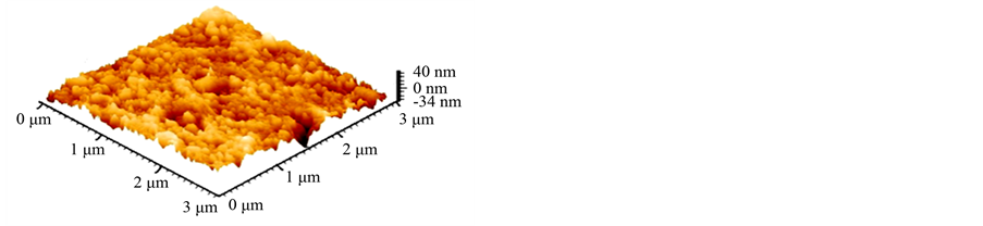
Figure 6 shows the Atomic force microscope images for the samples at three distances. Figure 6(c) at near distances from the graphite rod the center of the plasma will lead to a distortion of the samples surfaces, increase
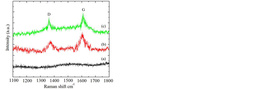
Figure 4. Raman spectra for the samples with distances from the Carbon rod (a) 14.1 cm, (b) 14.4 cm and (c) 14.7 cm.
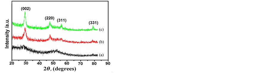
Figure 5. X-ray spectrum for the samples at three distance (a) 14.1 cm, (b) 14.4 cm and (c) 14.7 cm.
 (a) (b)
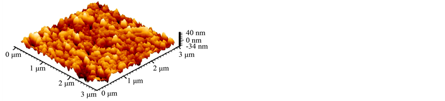 (c)
(c)
Figure 6. Atomic force microscope images for the samples at three (a) 14.1 cm, (b) 14.4 cm and (c) 14.7 cm.
in surface roughness and preventing the formation of grains and carbon nanotubes, whereas grains are well defined for the medium and far distances Which we will consider as optimum Figure 6(a) & Figure 6(b) [11] [12] .
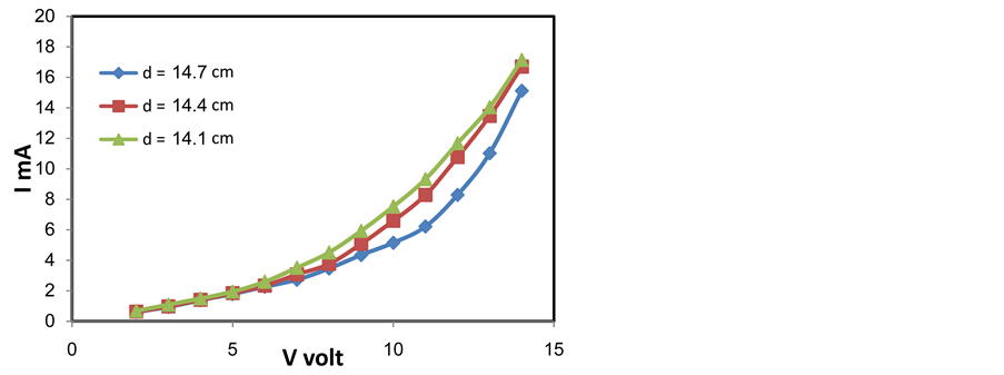
Figure 7. The I-V characteristics for Si-C junction with gold electrodes.
The I-V characteristics for Si-C junction with gold electrodes on the front and backsides of the junction are shown in Figure 7. It is very clear that the junction has a semiconducting behavior, which is a characteristic property of the zigzag carbon nanotubes I-V characteristics support our deduction and best curve is with distance 1.47 cm.
The study by scanning electron (SEM) and atomic force microscopes (AFM), X-ray and Raman spectra all shows that distance between sample and source of plasma sputtering source affecting the formation of CNT on the Si wafer .For near distance no formation of CNT , whereas it appears for medium and longer distances. This means that at closer distance high energy and high intensity plasma particles prevent the formation of CNTi.eit prevent the formation of the hexagonal C loops which is the essential unit of the graphite layer that forms the CNT, this effect decreased with increasing distance of substrate from the graphite rod which means that the distance between sample and source is a critical factor.
4. Conclusion
Distance between sample and source of plasma sputtering source affect the formation of CNT on the Si wafer. For near distance there is no formation of CNT, whereas it appears for medium and longer distances. This means that at closer distance high energy and high intensity plasma particles prevent the formation of CNT. This effect decreases with increasing distance of substrate from the graphite rod.
References
- Poole Jr., C.P. and Owens, F.J. (2003) Introduction to Nanotechnology. John Wiley & Sons, Inc., Hoboken.
- Seshan, K. (2001) Handbook of Thin-Film Deposition Processes and Techniques, Principles, Methods, Equipment and Applications. Noyes Publications/William Andrew Publishing, New York.
- Rümmeli, M.H., Bachmatiuk, A., Börrnert, F., Schäffel, F., Ibrahim, I., Cendrowski, K., Simha-Martynkova, G., Plachá, D., Borowiak-Palen, E., Cuniberti, G. and Büchner, B. (2011) Synthesis of Carbon Nanotubes with and without Catalyst Particles. Nanoscale Research Letters, 6, 303. http://dx.doi.org/10.1186/1556-276X-6-303
- Hofmann, S., Kleinsorge, B., Ducati, C., Ferrari, A.C. and Robertson, J. (2004) Low-Temperature Plasma Enhanced Chemical Vapor Deposition of Carbon Nanotubes. Diamond and Related Materials, 13, 1171-1176. http://dx.doi.org/10.1016/j.diamond.2003.11.046
- Gan, K.J., Chang, C.H., Lu, J.J., Lin, C.L., Su, Y.K., Li, B.J. and Yeh, W.K. (2011) Growth of Carbon Nanotube Using Microwave Plasma Chemical Vapor Deposition and Its Application to Thermal Dissipation of High-Brightness Light Emitting Diode. WCE 2011, London, 6-8 July 2011.
- Choi, Y.C., Bae, D.J., Lee, Y.H. and Lee, B.S. (2000) Growth of Carbon Nanotubes by Microwave Plasma-Enhanced Chemical Vapor Deposition at Low Temperature. Journal of Vacuum Science & Technology A, 18, 1864. http://dx.doi.org/10.1116/1.582437
- Jorio, A., Pimenta, M.A., Souza Filho, A.G., Saito, R., Dresselhaus, G. and Dresselhaus, M.S. (2003) Characterizing Carbon Nanotube Samples with Resonance Raman Scattering. New Journal of Physics, 5, 139.1-139.17.
- Bokova, S.N., Obraztsova, E.D., Grebenyukov, V.V., Elumeeva, K.V., Ishchenko, A.V. and Kuznetsov, V.L. (2010) Raman Diagnostics of Multi-Wall Carbon Nanotubes with a Small Wall Number. Physica Status Solidi (B), 247, 2827- 2830. http://dx.doi.org/10.1002/pssb.201000237
- Lehman, J.H., Terrones, M., Mansfield, E., Hurst, K.E. and Meunier, V. (2011) Evaluating the Characteristics of Multiwall Carbonnanotubes. Carbon, 49, 2581-2602. http://dx.doi.org/10.1016/j.carbon.2011.03.028
- Oddershede, J., Nielsen, K. and Stahl, K. (2007) Using X-Ray Powder Diffraction and Principal Component Analysis to Determine Structural Properties for Bulk Samples of Multiwall Carbon Nanotubes. Zeitschrift für Kristallographie, 222, 186-192.
- Zdrojek, M., Gebicki, W., Jastrzebski, C., Melin, T. and Huczko, A. (2004) Studies of Multiwall Carbon Nanotubes Using Raman Spectroscopy and Atomic Force Microscopy. Solid State Phenomena, 99-100, 265-268. http://dx.doi.org/10.4028/www.scientific.net/SSP.99-100.265
- Bellucci, S., Gaggiotti, G., Marchetti, M., Micciulla, F., Mucciato, R. and Regi, M. (2007) Atomic Force Microscopy Characterization of Carbon Nanotubes. Journal of Physics: Conference Series, 61, 99-104.