Journal of Sensor Technology
Vol.3 No.4(2013), Article ID:40952,9 pages DOI:10.4236/jst.2013.34016
Output Drifting of Vacuum Packaged MEMS Sensors Due to Room Temperature Helium Exposure
1Hanking Group Ltd., Shenyang, China
2ePack Inc., Ann Arbor, USA
Email: sparksdr@hanking.com
Copyright © 2013 Douglas Sparks et al. This is an open access article distributed under the Creative Commons Attribution License, which permits unrestricted use, distribution, and reproduction in any medium, provided the original work is properly cited.
Received September 26, 2013; revised October 28, 2013; accepted November 4, 2013
Keywords: MEMS; Helium; Resonator; Pressure Sensor; Pirani Gauge
ABSTRACT
Exposure of absolute pressure sensors, resonant microtube density, binary concentration sensors and chip-scale vacuum packaged pirani gauges to room temperature helium resulted in a gradual drift in sensor output. No effect was found for differential pressure sensors and pirani gauges vacuum packaged with ceramic or metal packages. The observed results apply to other vacuum packaged MEMS devices such as gyroscopes, voltage controlled oscillators, infrared and Coriolis mass flow sensors. Potential causes for this loss of hermeticity are discussed as well as application limitations for MEMS sensors.
1. Introduction
A variety of Micro Electro Mechanical Systems (MEMS) devices have been applied to measuring the flow rate [1,2] density and constituent concentration [3,4] and pressure [5-8] of gases. While many of these devices have been designed for use in air or oxygen in automotive and medical applications, a number of MEMS sensors have been applied to the measurement of gases such as hydrogen, helium, natural gas, nitrous oxide and others.
Kim et al. [9] found that helium and hydrogen could permeate CVD (Chemical Vapor Deposition) oxide sealed MEMS resonators at elevated temperatures resulting in a degradation of Q values. Annealing in a hydrogen or helium ambient at 170˚C - 400˚C was found to increase microcavity pressure, as did reliability testing at 100˚C in air due to the 5 ppm helium present in the atmosphere. The gradual cavity pressure increase was not observed after operating in air 3000 hours at room temperature. By sealing the CVD oxide plugs with an aluminum capping layer this group could prevent hydrogen permeation into the CVD sealed microcavities at elevated temperatures.
Sparks [10] found changes in resonator Q in the presence of helium at low temperature in sealed single crystal silicon microstructures. These effects were seen between 23˚C and 100˚C after and during helium exposure at relatively low pressures of 140 KPa to 380 KPa. Resonator Q changes were not observed for hydrogen, argon, nitrogen, methane, carbon dioxide, sulfur hexafluoride and air [4,10]. Only helium, not hydrogen was found to permeate the silicon chip-scale MEMS resonator packages in that study.
In the current study the reliability of various MEMS vacuum sealing interfaces and packaging methods of a number of different MEMS devices were studied in more detail using room temperature helium pressurization. MEMS pressure sensors, pirani gauges and resonant microtubes used to make Coriolis mass flow, density and binary concentration sensors were examined for stability during exposure to helium.
2. Experimental Procedure
To examine a wide variety of MEMS packaging methods and materials, commercially available and experimentally fabricated devices were tested. The MEMS wafer and devices were fabricated at four different cleanroom facilities using four different types of wafer level bonding processes and two discrete vacuum package sealing methods. The commercially available sensors are shown in Figure 1. The large microfluidic resonator chip (middle) and packaged device (top middle) [4,10,11] uses a resonating silicon tube that is vacuum sealed with reflowed glass. All of these resonators employed thin film getters
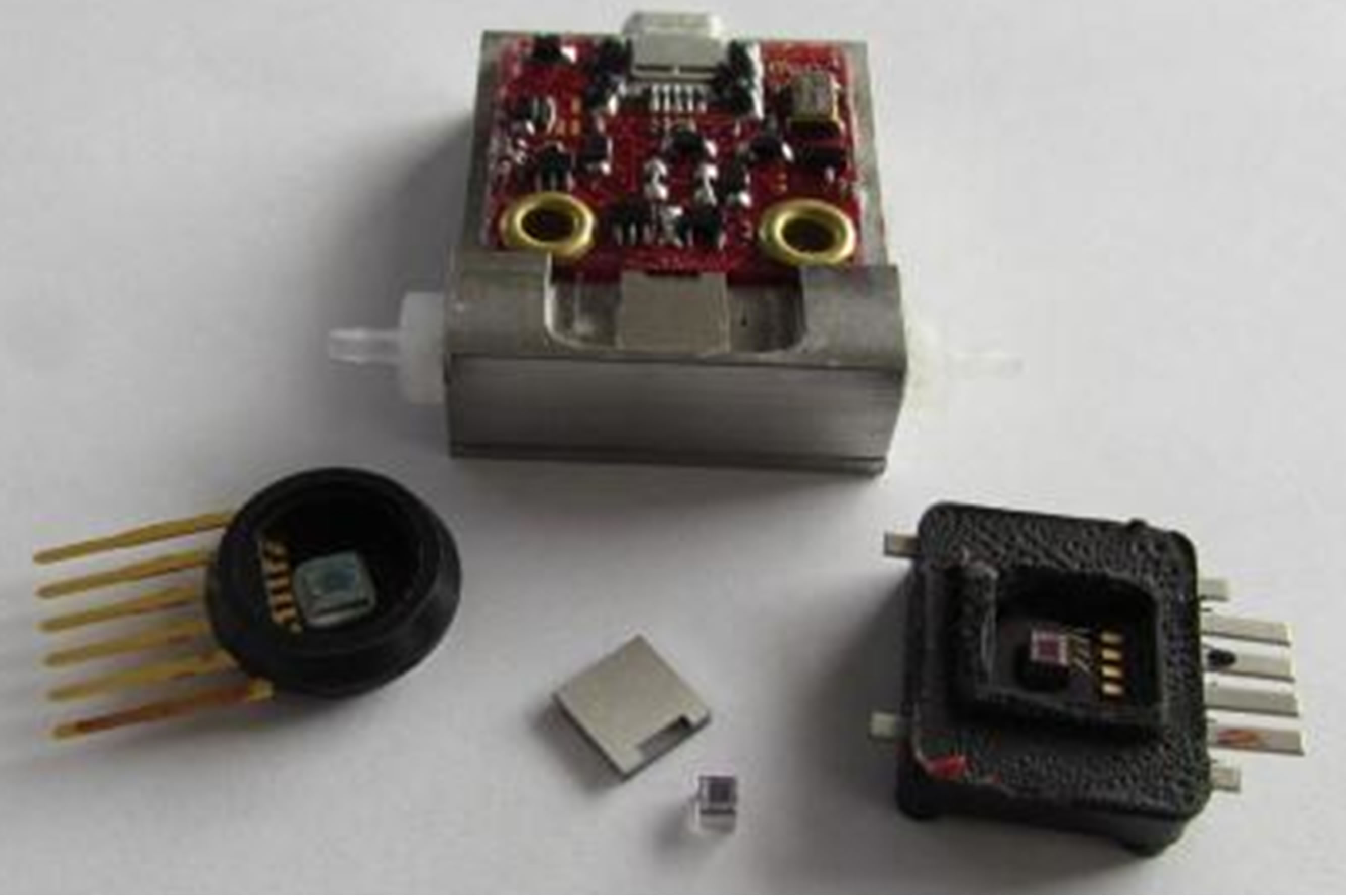
Figure 1. The commercially available pressure sensors and microfluidic resonator.
to obtain low initial, cavity pressures (1 mTorr). The metal getter film coated the entire top inner surface of the silicon cavity. To investigate potential helium related effects on pressure sensors, three different pressure sensors were also tested in this study; a Freescale manifold absolute pressure sensor, MPX4200A (round left) in Figure 1 that is made using two silicon wafers bonded with reflowed glass [5], a Delphi manifold absolute pressure sensor (square right) that forms its vacuum reference using silicon to glass anodic bonding [8], and finally a Delphi differential silicon on glass pressure sensor. The glass thickness in the Delphi chip is 1500 microns, while the silicon diaphragm is only 12 microns thick. The Delphi pressure sensors are just Wheatstone bridges with no amplification. The Freescale pressure sensor gives an amplified output, not just a Wheatstone bridge offset. It should also be noted that the Freescale diaphragms were coated with a silicone gel while the Delphi diaphragms in this study were not coated.
MEMS pirani gauges [12,13] were also tested under helium exposure. As shown in Figure 2 the experimental pirani gauges were chip scaled packaged (CSP) using gold-silicon eutectic wafer bonding (bottom) as well as vacuum packaged in ceramic combo packages using goldtin solder reflow to a gold plated Kovar lid (left) and with welded round Kovar lid to a Kovar TO-type package (right). Kovar is a Fe/Ni/Co alloy with a low thermal expansion coefficient, commonly used for packaging silicon. The round Kovar lids were 250 microns thick as were the square lids used with the ceramic packages. A solder preform made of eutectic gold-tin was used to join the Kovar lid to the gold metallized ceramic package. The bottom portion of the ceramic package was 500 microns thick. The 1625 micron thick base of the metal package has four wires that use reflowed glass for wire feedthrough insulation. The packaged pirani gauges did not employ wafer bonded capping, while the chips scale pirani devices had a 500 micron thick silicon capping layer attached with a gold-silicon eutectic seal using a silicon nitride insulating layer around the feedthroughs, see Figure 3(d). The chips scale and ceramic package employed thin film getters while the welded metal package did not. The pirani gauge wafers were fabricated in the University of Michigan cleanroom. Figure 3 illustrates the various chip-scale package sealing methods and seals examined in this study, and Figure 4 illustrates how the discrete ceramic and metal packages vacuum seal the MEMS pirani gauges.
High pressure helium exposure was done using a gas cylinder and brass pressure container as shown in Figure 5. For this study resonator Q, pressure diaphragm deflec-
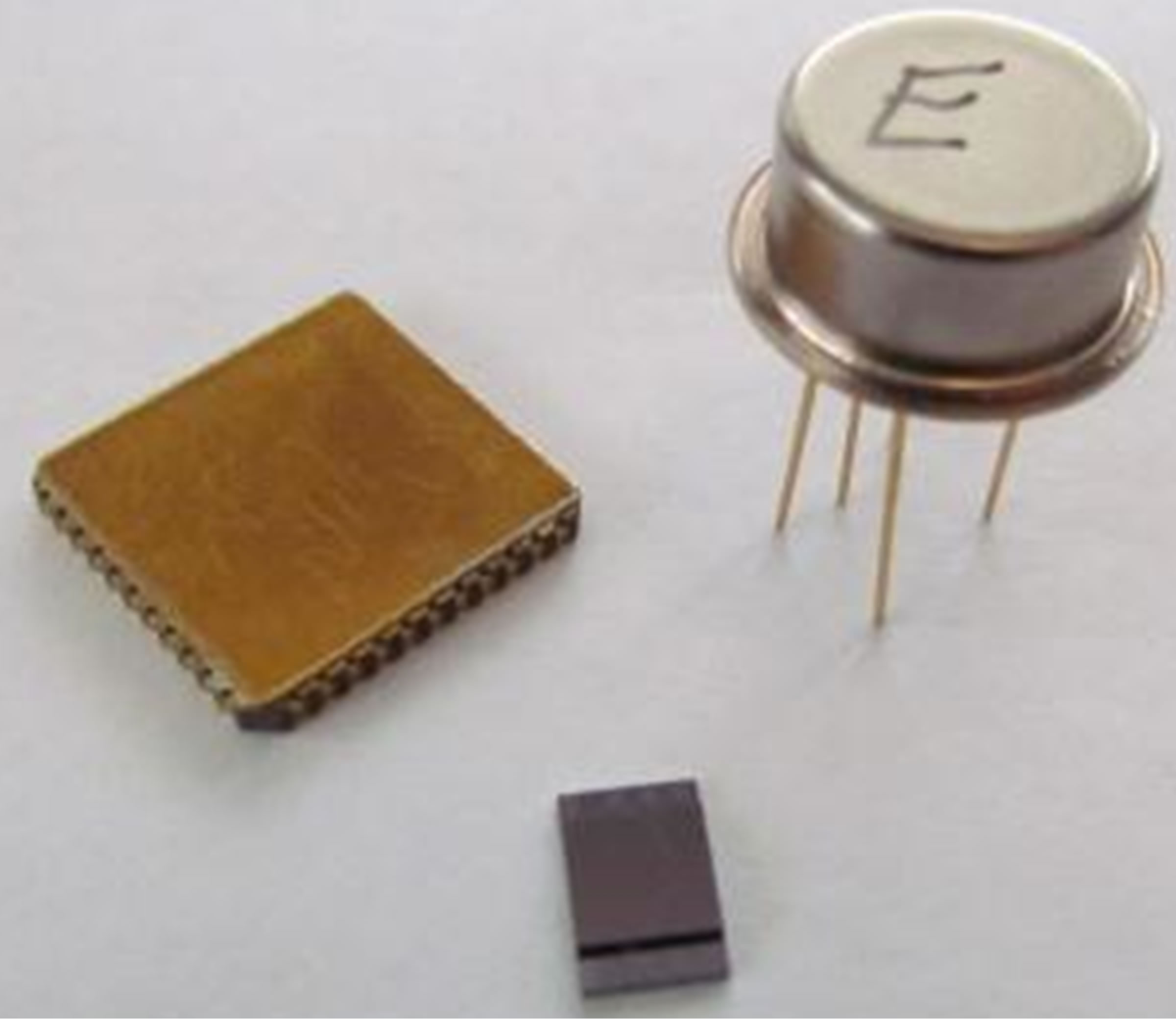
Figure 2. The experimental pirani gauges tested in this paper.
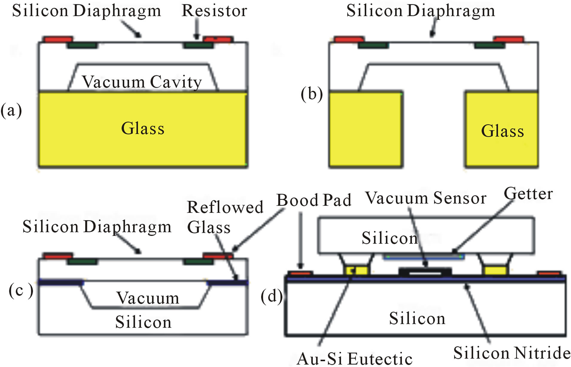
Figure 3. The wafer-level chip sealing methods used in this study: anodically bonded (a) absolute pressure sensor and (b) differential pressure sensor, (c) frit reflowed glass sealed pressure sensor and the (d) Au-Si eutectic bonded pirani gauge.
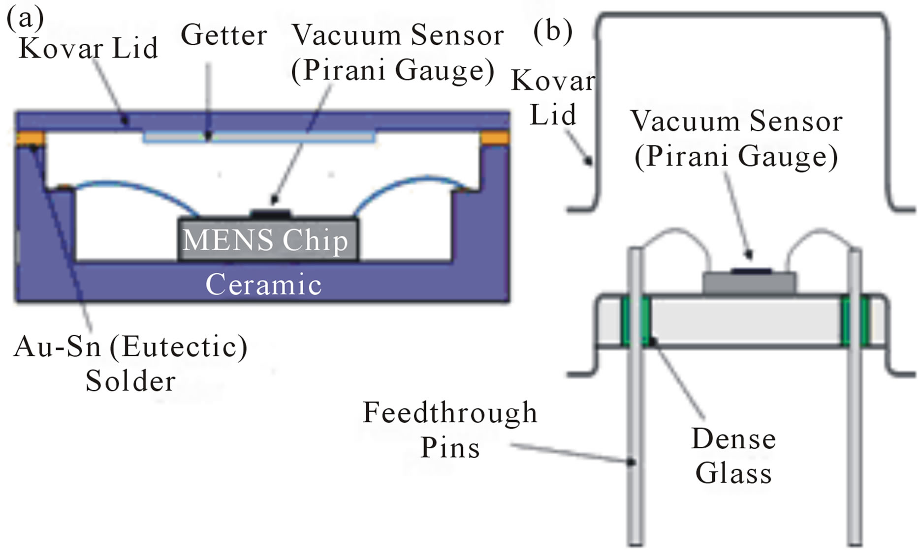
Figure 4. Ceramic (a) and TO-Metal (b) MEMS packages.
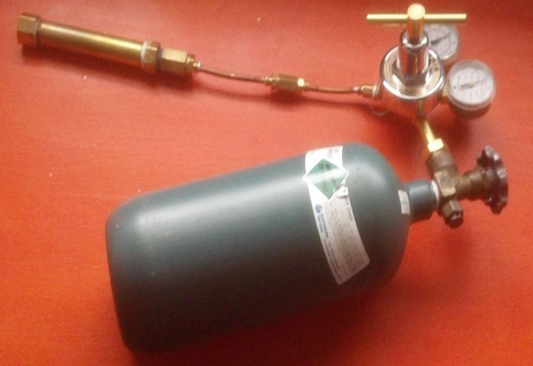
Figure 5. The helium pressurization system.
tion measured via piezoresistive bridge offset and thermal impedance of the pirani gauge were used to monitor pressure changes of the different MEMS devices.
All MEMS devices, except the silicon direct bonded resonant tubes, were pressurized in pure helium using the system shown in Figure 5. When testing the hermeticity of the resonating silicon tube, sealed using silicon direct bonding, the interior of the silicon tubes were pressurized by attaching the packaged device (top center of Figure 1) to the helium using tubing as illustrated in Figure 6.
3. Experimental Results
3.1. Resonators
Both solid resonators and silicon tube resonators exhibited a loss of vacuum during exposure to helium, a total of 22 resonator parts all showed a rapid reduction in Q after exposure to pressurized helium. Figure 7 shows how the Q value decreased from continued helium exposure at 380 KPa at room temperature. The silicon direct bonded tubes were pressurized, while for the solid resonator the entire MEMS chip was immersed in helium. A Q value was measured over time to generate each data point in Figure 7, after which the MEMS chips were re pressurized with helium. This Q change corresponds to a pressure increase from 1 mTorr to over 100 Torr [14] after just 48 hours of helium exposure. The buildup of helium also caused a frequency drift with helium exposure time in the resonator as shown in Figure 8. A maximum frequency change of 83 Hz was observed due to helium exposure at 380 KPa. Of the 22 resonators tested in helium in this study at various pressures, 100% of resonators exposed to pressurized helium exhibited a Q decrease.
The final resonator experiment involved determining how sensitive these resonators were to lower helium concentrations. Since diffusion is enhanced by temperature the resonators were exposed to helium nitrogen mixtures and compressed air at 85˚C, which are at the high end of most operating conditions for MEMS products. A gas
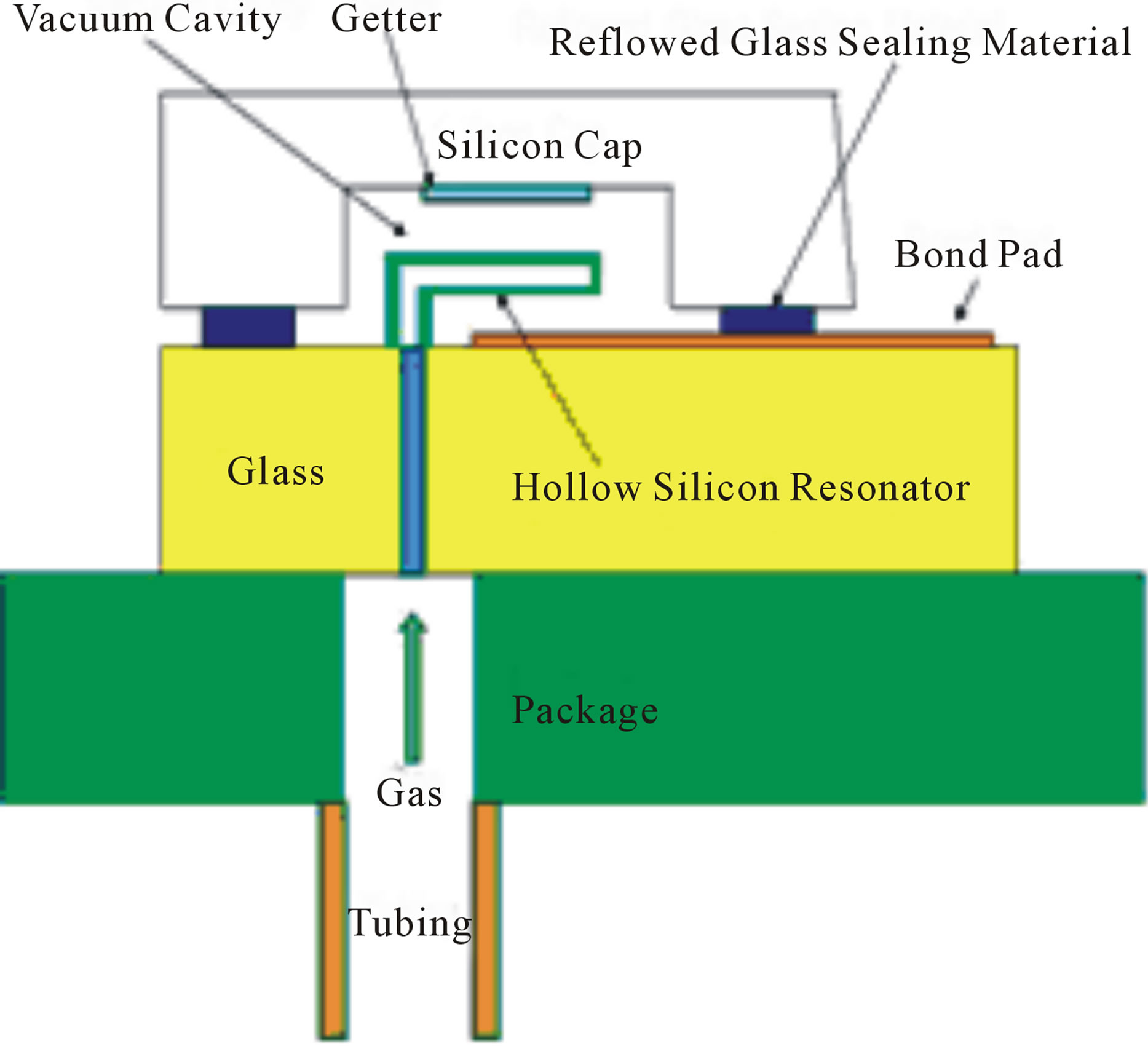
Figure 6. An illustration of how the direct silicon fusion bond of the packaged resonating tube was helium pressurized via the package tubing fitting.
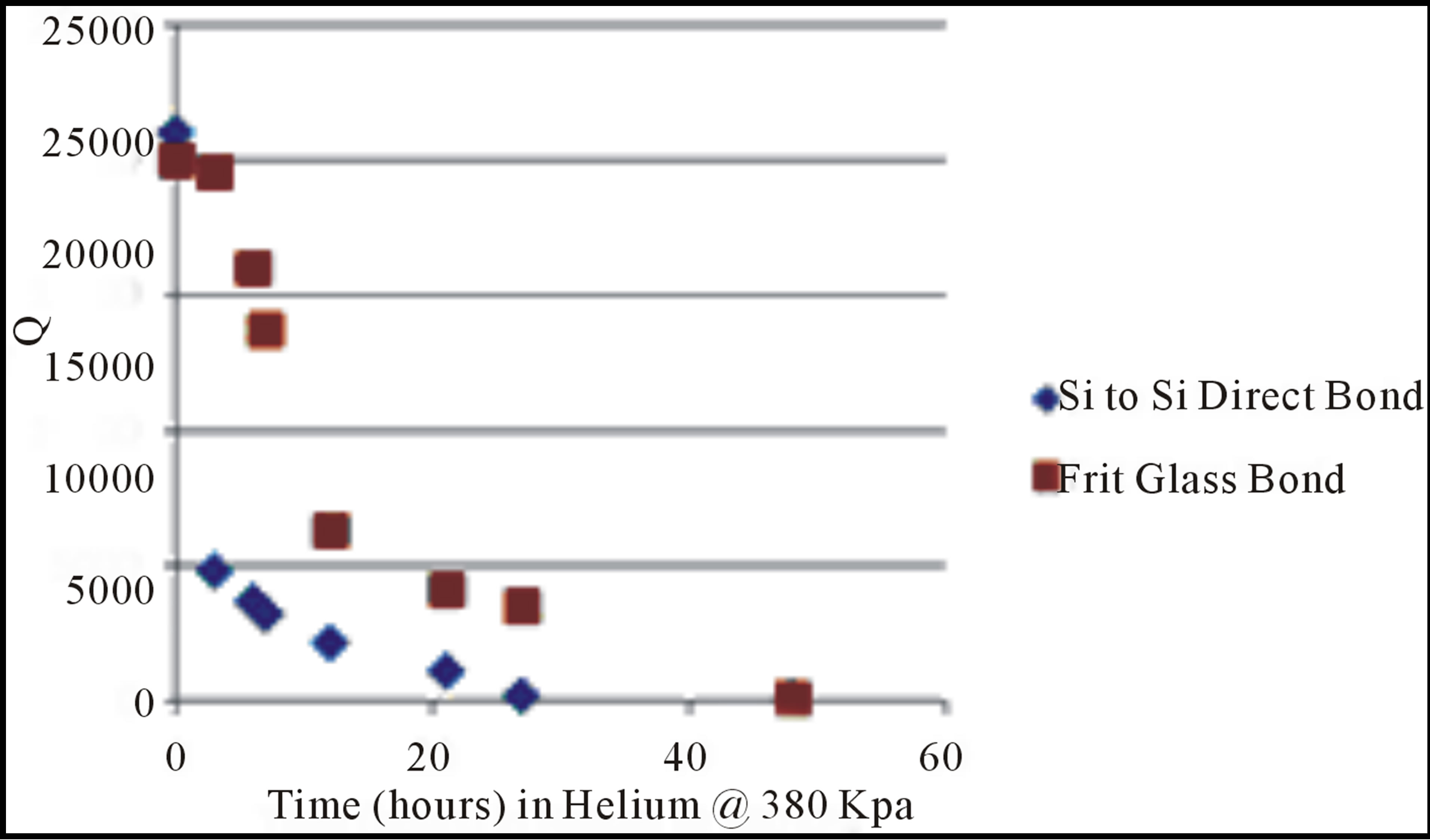
Figure 7. The change in resonator Q due to helium exposure at 380 KPa of the reflowed glass seal and direct silicon fusion bond seal of the resonating tube.
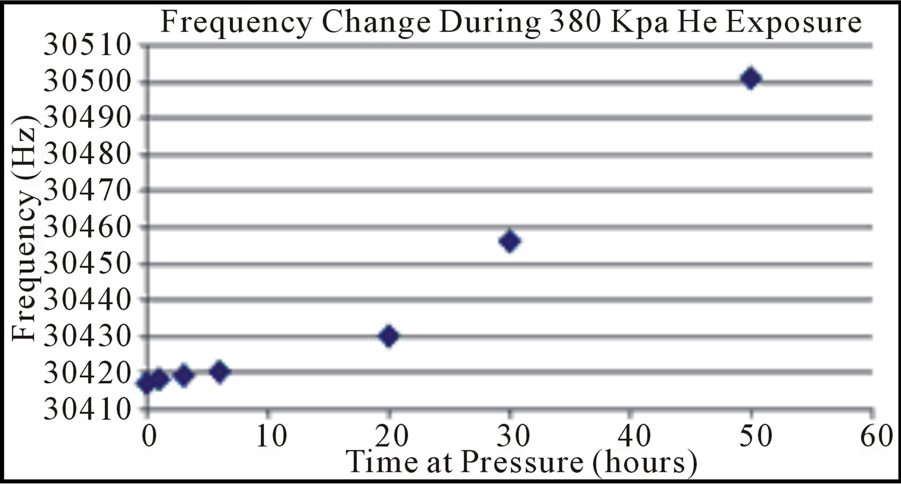
Figure 8. The change in resonant frequency form room temperature helium exposure.
mixture with just 100 ppm helium in nitrogen was used to pressurize only the interiors of the thin silicon tubes by using the package fluid connector fittings shown in the top middle of Figure 1 and in Figure 6. After one week at 85˚C and 380 KPa, the Q values began to gradually decrease for these resonators. No Q change was noted after more than one month for the same types of parts using compressed air at 85˚C, 380 KPa, which has 5 ppm of residual helium.
3.2. Pressure Sensors
The next set of experiments involved pressure sensors. The zero pressure bridge offset of an absolute pressure sensor is a measure of diaphragm deflection and hence cavity pressure [6,7]. An example of this is that the bridge offset shifts down by 40 to 50 mV after vacuum anodic bonding for the Delphi Wheatstone bridge absolute pressure sensors. The helium testing began at 380 KPa, for 24 hours, a condition that caused a shift in the resonators. Unlike the resonators, no change in zero pressure offset of the pressure sensors were noted for this helium pressure and soak time. For the next test the helium pressure was then increased to 415 KPa. Figure 9 shows that a drift over time in the zero pressure sensor output for the helium immersed parts, at 415 KPa, versus that of the control group was observed. Each point uses the average for 5 pressure sensors. The zero pressure offset shift is the difference between the average bridge or sensor output of the helium immersed parts and the controls that were left in air at atmospheric pressure and room temperature. The standard deviation of the controls ranged from 0.006 to 0.007 V, while the standard deviations of the helium immersed samples ranged from 0.033 to 0.05 V. The Freescale, frit glass bonded pressure sensor outputs ranged from 2.299 to 2.315 V at room temperature and pressure prior to helium exposure. At the end of the helium soak the Freescale pressure sensors zero pressure outputs range from 1.905 to 2.003 V. Both the Freescale monolithic absolute pressure sensor and Delphi Wheatstone bridge absolute pressure sensor showed a gradual linear drift in the zero pressure offset over helium exposure time. This denotes an increase in the cavity pressure of the vacuum reference which causes a change
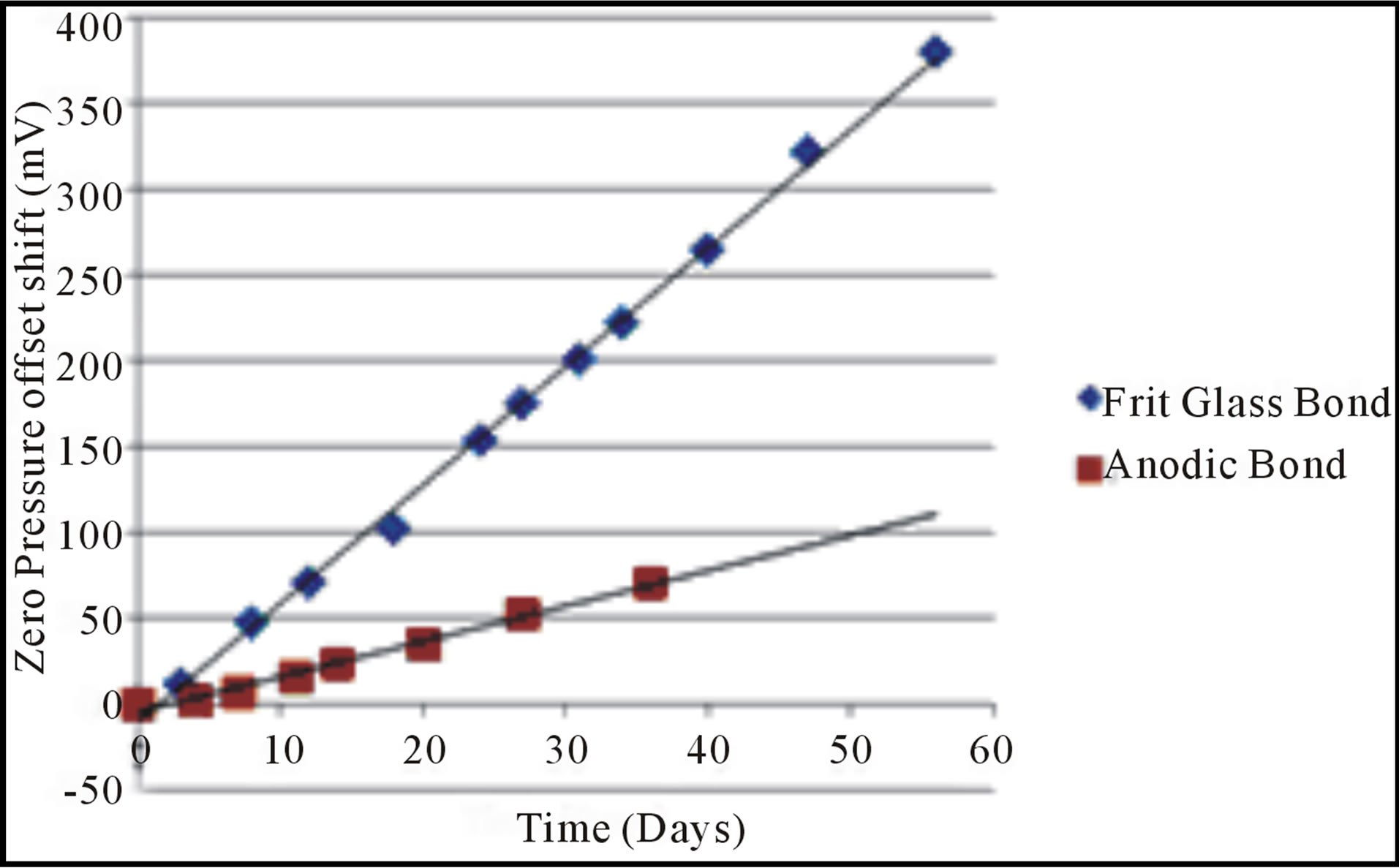
Figure 9. The absolute pressure sensor output change due to prolonged room temperature helium exposure at 415 KPa.
in the deflection of the piezoresistors in the bridge [6,7]. Control absolute pressure sensors stored in air at the same pressure showed no change in the zero pressure offset. The differential Delphi pressure sensors showed no change due to the same helium exposure. The anodically bonded Delphi absolute pressure sensor is of most interest since there is no sealing material, only the relatively wide 300 micron, glass-silicon interface around the vacuum reference cavity.
Figure 10 shows that a gradual recovery of the Wheatstone bridge offset was noted at the completion of the helium testing. The offset difference of an anodically bonded Delphi absolute pressure sensor sample, held in room temperature air, began to slowly return to the original pre-helium soak values. After 227 days in room air, the bridge offset difference of the anodically bonded pressure sensors had reversed the shift by 60 mV, going from 73 mV to just 13 mV offset from the starting bridge offset voltage, or 82% of the helium induced change.
3.3. Pirani Gauges
To examine other means of packaging MEMS sensors, pirani gauges were packaged with three different methods, wafer-level, chip scale packaging, welded metal TO lids, and ceramic packages with soldered lids were first pressurized with helium. The pressure starting point for this test was 275 KPa of helium for 11 hours. As shown in Table 1 no change in thermal impedance and hence cavity pressure was noted after this. Additional CSP and metal packaged parts were added and the pressure and helium soak time was increased to 415 KPa for 90 hours. No change in cavity pressure for all three types of packages was noted under this testing condition. The thicker 500 μm silicon caps with the gold-silicon eutectic seal was an effective barrier for the chip scale packages at helium pressures of 275 - 415 KPa at room temperature. Finally the pressure and helium soak time was increased to 690 KPa for 408 hours. The average cavity pressure of the chip scale packaged pirani gauges increased by 1.471 Torr after this treatment, while the ceramic and metal packages showed no significant change in thermal im-
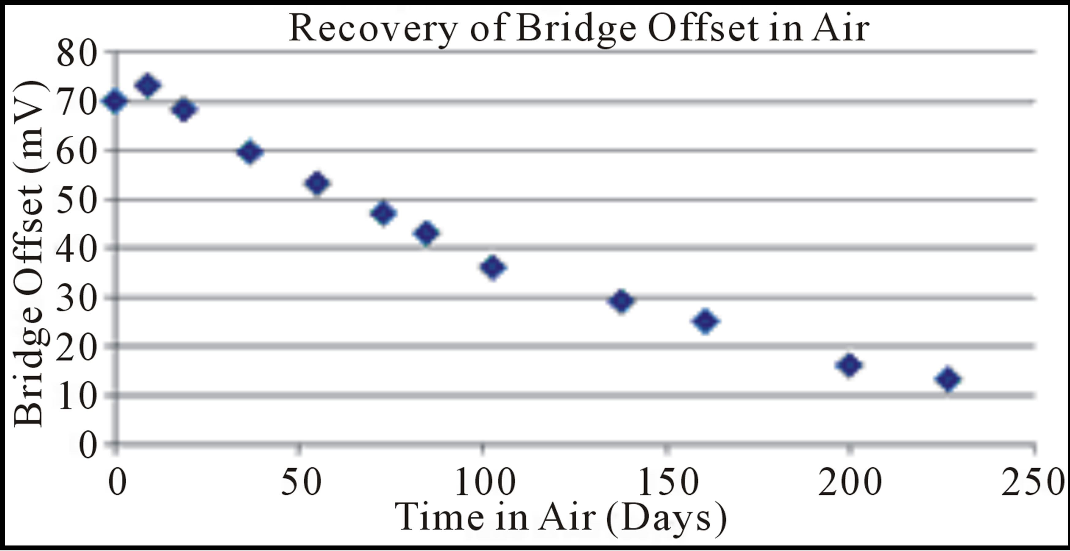
Figure 10. The change in the bridge offset between the helium exposed sensors and controls after the conclusion of the helium testing at room temperature in air.
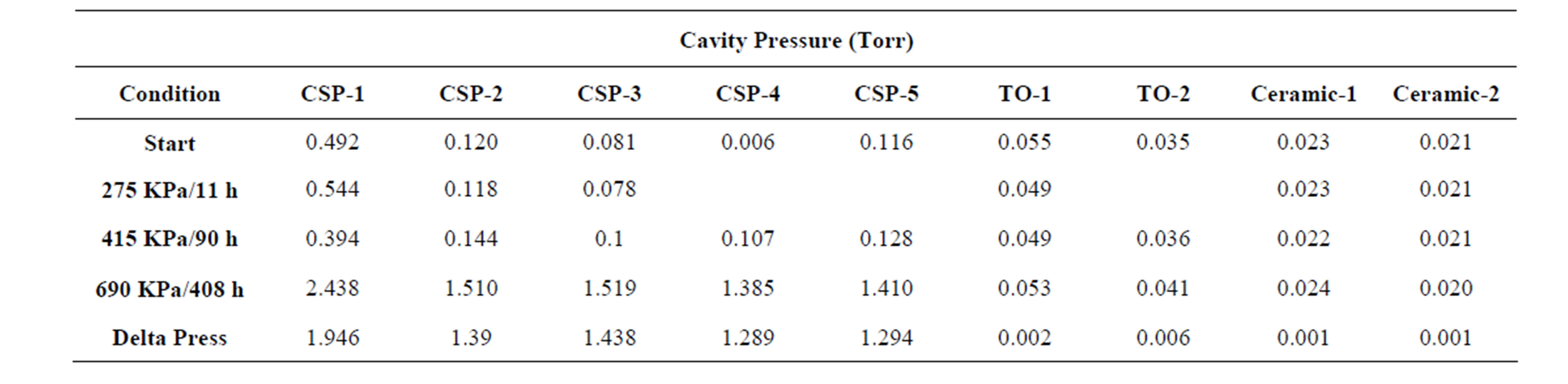
Table 1. Pirani gauge output in pressure, before and after room temperature helium exposure.
pedance and hence internal pressure, as shown in Table 1.
4. Discussion
The MEMS devices used in this study to investigate room temperature permeation had differences in materials and sealing methods as well as helium sensitive functional elements. The resonators needed only 0.5 to 2 hours of exposure to helium at 140 to 380 KPa to exhibit a lower Q. The absolute pressure sensors required several days of helium pressures of 415 KPa for a noticeable shift in the zero pressure bridge offset. The wafer-level packaged pirani gauges needed many days of helium immersion at 690 KPa to exhibit a thermal impedance change indicating an increase of pressure in the silicon microcavity. Ceramic and steel vacuum packaged pirani gauges did not showed an indication of helium permeation under these test conditions.
Figure 10 indicates that this helium effect is reversible for the absolute pressure sensors, the output of the sensors can shift in both directions depending on the helium exposure duration. The same reversible effect for Q was observed with the resonators in an earlier study [10].
Table 2 summarizes the different wafer and package level vacuum sealing materials used in this study, and Kim et al. [9], as well as the packaging methods and results with regard to helium permeation. All chip-scale vacuum packaging methods eventually had a helium ingress problem while the two discrete packaging methods using ceramic and metal packages did not. Even wafer level bonding methods with no sealing material, direct fusion bond and anodic bonding, were not hermetic in the presence of pressurized helium at room temperature. Silicon is the common material (12 μm to 500 μm thick) for the leaking parts both the anodically bonded pressure sensor and all silicon direct fusion bonded microtube both allowed helium to pass into the microcavity and do not utilized sealing layers during wafer bonding.
4.1. Sensor Output Drift
For resonant tube density meters, the density of a fluid ρ in a vibrating tube is given by the expression:
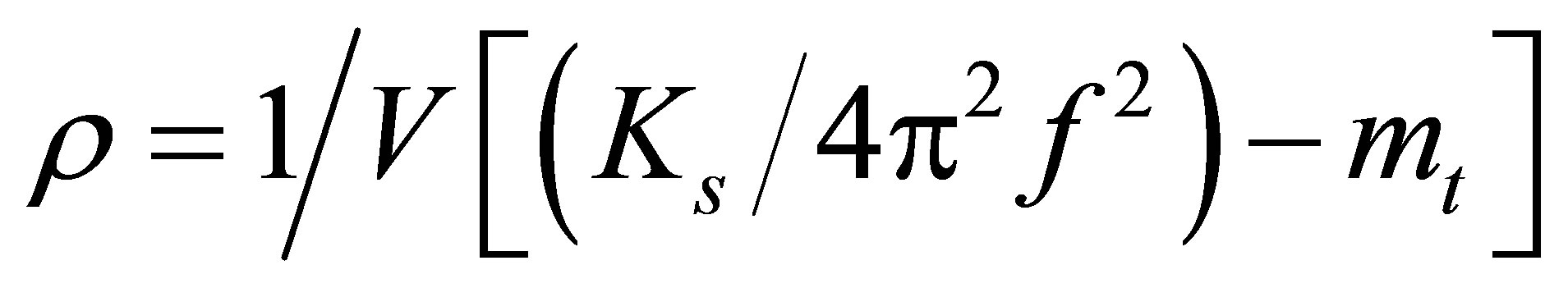 (1)
(1)
where V is the internal volume of the resonant tube, mt is tube mass, Ks is the spring constant of the tube and f is the resonance frequency of the tube. As can be seen by the expression above, the density is inversely proportional to the square of the resonance frequency. A frequency shift of 83 Hz, as was observed due to 48 hours of helium exposure at 380 KPa, results in a large density measurement error. Just a short 1 hour exposure to helium at 380 KPa resulted in a 1 Hz shift and which corresponds to a density meter output shift of 0.143 kg/m3. Chemical concentration of binary solutions can be measured using this mass-based approach. Any shift in resonator frequency due to helium permeation causes a density and concentration error in these sensors. Twenty hours of exposure to 380 KPa of helium caused a 13 Hz frequency shift resulting in a density error of 1.86 kg/m3, which is greater than what is found going from 100% nitrogen to 100% hydrogen at 101 KPa. This illustrates the type of concentration error that helium exposure can induce in this resonating sensor. While MEMS density meters can be used with many gases [4], applications with helium mixtures or impurities like some welding cover gases, deep sea diving and natural gas monitors [15] should be avoided.
Resonant Coriolis mass flow sensors [1,2] also use frequency to arrive at a mass flow rate. The basic function of an ideal resonating Coriolis mass flow sensor can be expressed by Equation (2). The mass flow rate q is given by:
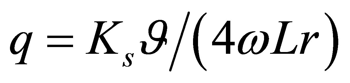 (2)
(2)
where, Ks angular spring constant of the flow tube, ![]() is the twisting angle of the tube,
is the twisting angle of the tube, ![]() is the resonance frequency, L is the length of the tube and r is the radius of the U-bend of the tube. Therefore, the mass flow rate is directly proportional to the twisting angle and inversely proportional to the resonance frequency. Any shift in frequency due to helium permeation into the vacuum cavity leads to a mass flow error. As Figure 7 showed the resonator Q can drop from 20,000 to below 100 after helium exposure. For both flow and density sensors the reduction
is the resonance frequency, L is the length of the tube and r is the radius of the U-bend of the tube. Therefore, the mass flow rate is directly proportional to the twisting angle and inversely proportional to the resonance frequency. Any shift in frequency due to helium permeation into the vacuum cavity leads to a mass flow error. As Figure 7 showed the resonator Q can drop from 20,000 to below 100 after helium exposure. For both flow and density sensors the reduction
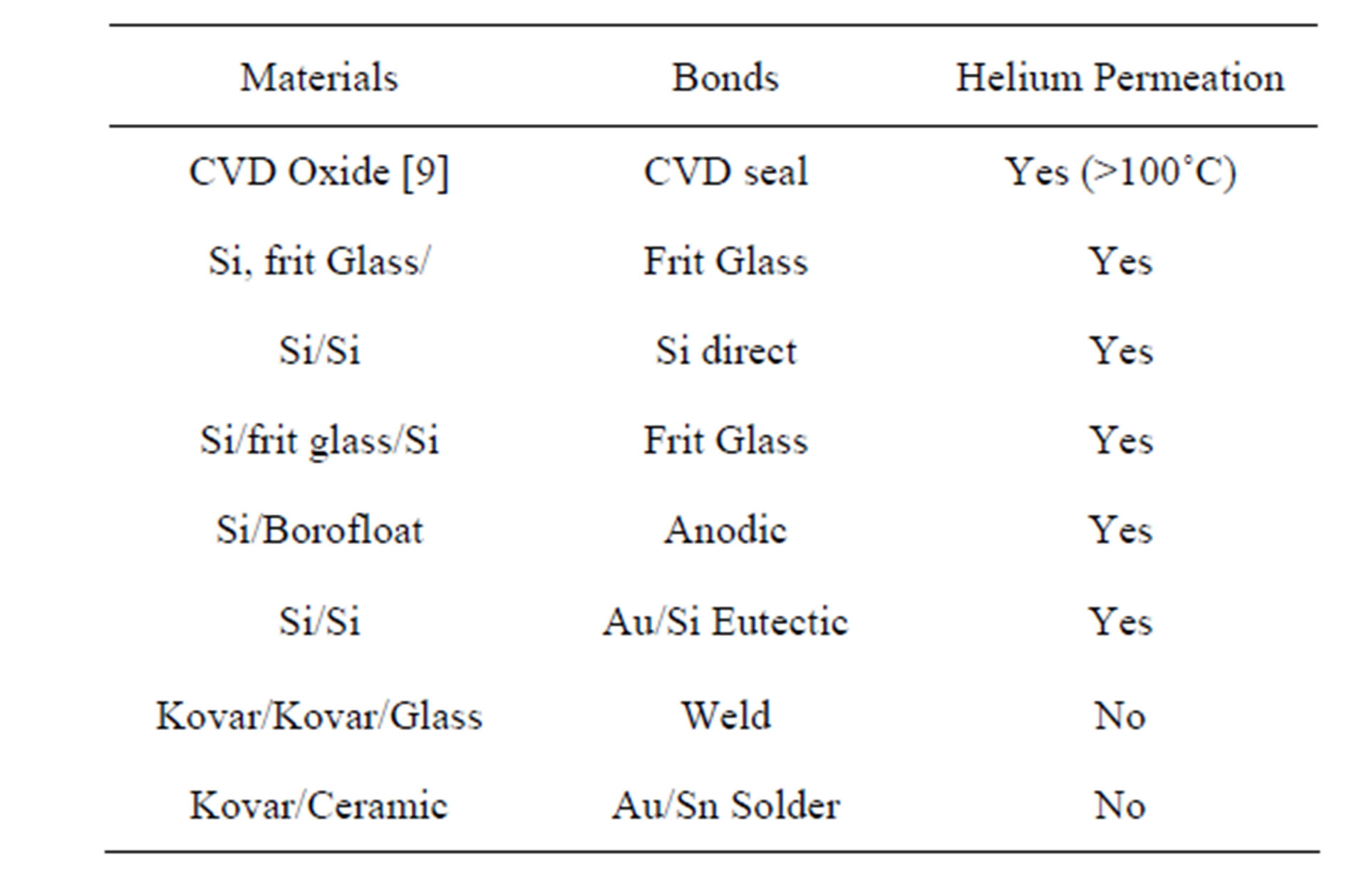
Table 2. Helium permeation with respect to the various sealing methods and materials.
in the Q can eventually lead to an inability of the circuitry to track the resonator output signal peak resulting in another failure mode for these devices due to helium ingress into the vacuum sealed cavity.
The results observed for the two types of absolute pressure sensor clearly indicate that these types of MEMS devices, sealed with reflowed glass and anodic bonding, cannot be used in helium containing gases without a helium impermeable corrugated metal diaphragm. Figure 11 shows how the diaphragm deflection, indicated in Figure 9 caused a pressure error over time due to helium exposure at 415 KPa. Backside sense absolute pressure sensors with their reference vacuum cavity on the topside of the diaphragm may also have the same problem. The observation that both the Kovar welded and soldered lids did not allow helium to enter into the vacuum cavity at (100 psi) indicates that a helium compatible metal diaphragm is a possible solution for absolute pressure sensors. Differential or gauge pressure sensors are not affected by the presence of high pressure helium, although other factors like burst pressure precautions should still be taken into account. The negative results from the differential pressure sensors indicates that pn junction or dielectric layer leakage currents due to helium exposure are not responsible for the sensor output shift observed with the absolute pressure sensors.
In addition to the MEMS devices tested in this study, other MEMS sensors and actuators, fabricated with wafer level packaging techniques and materials may be sensitive to helium hermeticity problems. As Kim et al. showed [9], CVD vacuum sealed MEMS devices, used for voltage controlled oscillators, can have a problem with the 5 ppm helium present in the atmosphere at the high end of the device operating temperature which can range from 85˚C to 150˚C for automotive, industrial and aerospace devices. This was due to the ingress of helium and hydrogen through CVD oxide plugs although both hydrogen and helium could diffuse through the epi/poly silicon CVD layer at higher temperatures as well.
Infrared sensors like bolometers, thermopiles and chemical sensors are vacuum packaged using germanium and silicon lids and could be subject to helium performance degradation. Infrared (IR) imaging and chemical sensors are being packaged at the wafer level using silicon [16]. Silicon capping wafers are being attached to sensing array wafers with low temperature metal joining methods like solder and eutectic bonding [12,13,16,17]. Helium diffusion due to sensor exposure to natural gas or even air could over time lead to an accumulation of helium in the vacuum sealed microcavity. This will result in interference at the helium absorption wavelengths shown in Table 3 [18]. If helium is diffusing through silicon at room temperature then even ceramic packages that use polished silicon lids may present an absorption problem. Further tests with silicon, germanium and various glasses will be needed to find out if helium, neon or hydrogen can diffuse through these window materials.
Vacuum packaged resonating MEMS gyroscopes and voltage controlled oscillators may also have a long-term drift problem when operated in air if chip-scale packaging methods are employed. This has been demonstrated by Kim with CVD sealed devices [9]. Enclosing these devices in ceramic or metal packages with Kovar lids, like those shown in Figure 2, can be used to prevent this long-term reliability issue.
Care must be taken when applying MEMS technology to applications dealing with helium and mixtures containing helium. Helium is used as welding cover gases, diving gases, airships, and semiconductor processing including MEMS wafer processing. MEMS devices have been proposed for space exploration, including Jupiter and Saturn with helium containing atmospheres [19].
Sensing pressure, density, composition and flow rates of natural gas could lead to device output drift due to low concentration of helium, up to 7%, in natural gas [15].
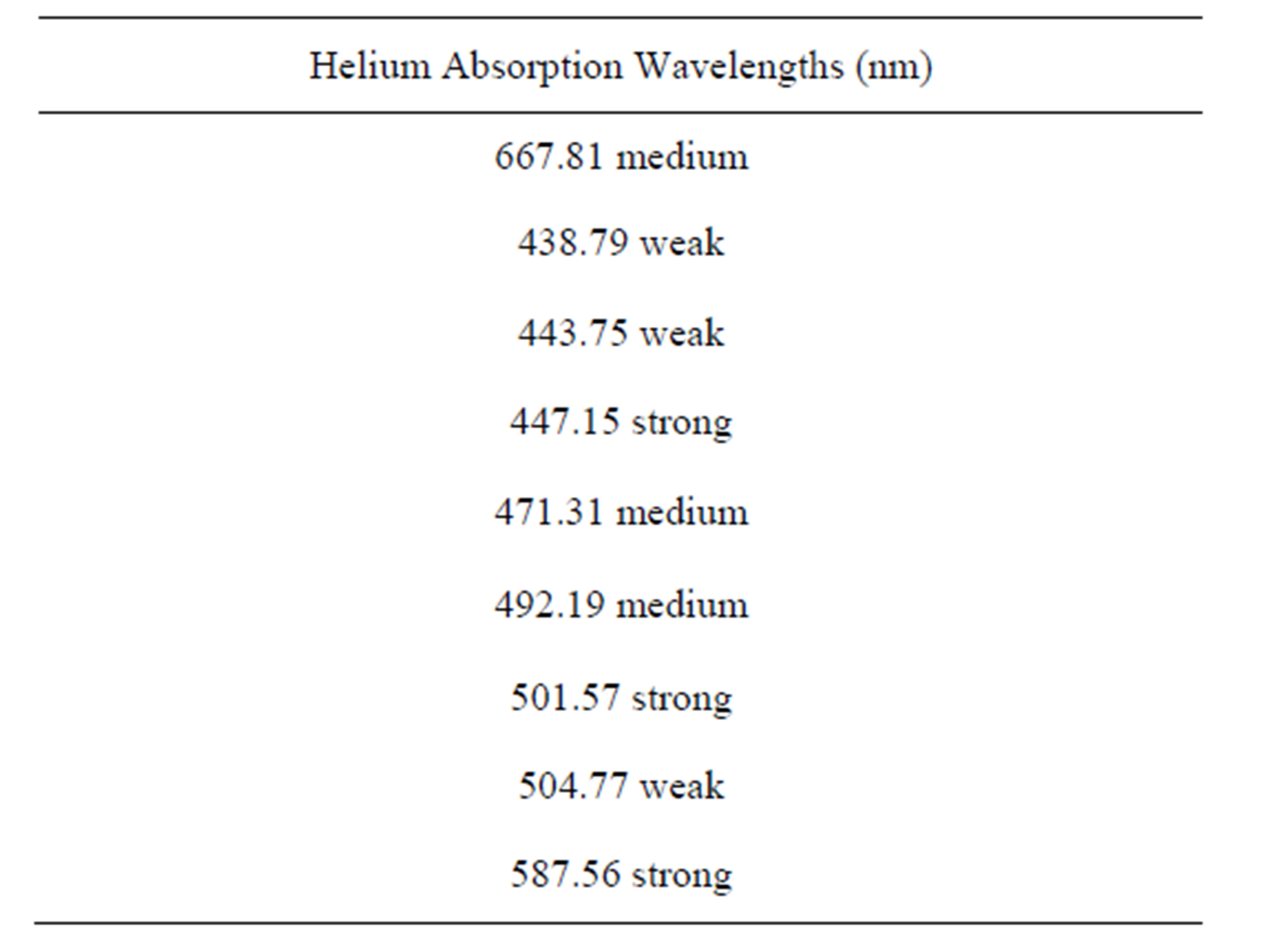
Table 3. Helium absorption peaks.
Finally helium bomb leak testing [20] could result in a long term drifting of devices that may have passed the initial leak test. Helium exposure can adversely affect unprotected vacuum sealed MEMS device, while differential pressure sensors and air or argon damped devices like accelerometers and RF switches should not be impacted by a light gas ambient.
4.2. Causes of Helium Permeation
Helium permeation can be caused by leakage through the wafer bonding interface due to defects and nonplanar surfaces as well as potentially by diffusion through the thin walls on the MEMS chip. While hermeticity problems due to particle related defects and voids can lead to leaks, this would not be an expected cause in four different wafer fabs with all four wafer level bonding methods. The permeation of helium has also been observed with three different MEMS devices: resonators, absolute pressure sensors and pirani gauges. Reflowed glass voids and wafer surface roughness [21,22] could be a path of helium migration for the anodic and direct bonded surfaces. One would expect that the glass reflow and eutectic bonded wafers would not present a helium migration path due to surface roughness since the sealing material would conform to the wafer surface irregularities.
Effusion rates were first measured by Thomas Graham back in 1829. He noted that the effusion rate of various gases is inversely proportional to the square root of the molecular masses of the gases. Graham’s law of effusion explains why a narrow channel or relatively tight seal may be leak proof to air or argon, and yet fail to hold lighter gases like hydrogen or helium. Table 4 lists the molecular mass and Van der Waal radii of various gases. Based on molecular weight both helium and hydrogen should effuse through wafer bond interface defects and gaps. Perhaps the Van der Wall radii is more critical for effusion through nanometer sized gaps, in which case helium would effuse through chip scale packages interfaces with more ease than hydrogen.
The resonators and pirani gauges have shown no sign of pressure change after years of storage in air (101 KPa) at room and elevated temperatures [10,13]. An earlier resonator study [10] found that the Q of the CSP resonators
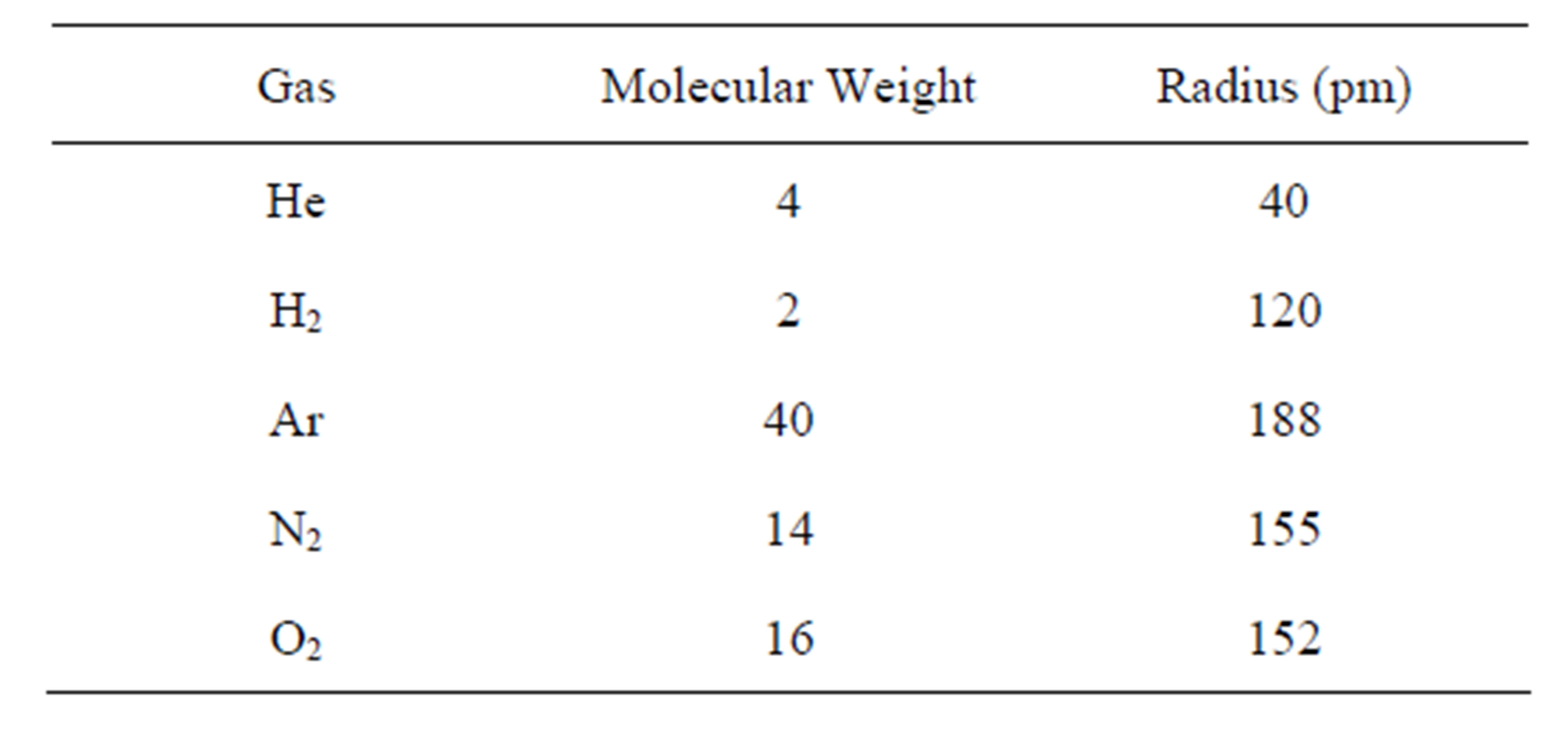
Table 4. Gas molecule comparison.
shown in Figures 1 and 6 could be degraded by 1 hour of helium exposure at 300 KPa but did not changed after 500 hours of exposure to 300 KPa hydrogen or immersion in argon and forming gas (4% H2 96% N2) at 790 KPa for 48 hours. These differences in Q impact suggests that classical effusion through an leakage path is not at work in this case. It is possible that the hydrogen is reacting with water vapor or hydroxyl molecules on the silicon, glass or oxide surfaces of these bonding interface imperfections, while helium does not react with this surface, and that the effusion path through these surface or seal imperfections is too small for argon, nitrogen and oxygen.
Diffusion of hydrogen through metal has led to pressure sensor output changes over time. Swanson [23] observed that MEMS-based pressure transmitters using corrosion resistant 25 to 50 micron thick, metal diaphragms failed in hydrogen after 30 - 60 hr when the diaphragms were made of high nickel content Hastelloy and Monel. Hydrogen diffused through the metal diaphragm and gas pressure build up lead to bubble formation in the silicone oil surrounding the MEMS pressure sensor which causes output errors. He noted that the hydrogen permeation effect increased exponentially with temperature, as a square root factor with pressure and inversely decreased with the thickness of the diaphragm. A passivation chromium oxide layer and plated gold layer on the surface of the metal diaphragm greatly improved the resistance to hydrogen permeation. No hydrogen permeation failures were seen after much longer exposure times with 316 stainless steel diaphragms under the same conditions. A change in diaphragm material solved this hydrogen diffusion related pressure sensing problem.
This study shows that diffusion of helium through single crystal silicon is a potential alternative to effusion through an interface defect. The metal TO packages employ glass feedthroughs between the wires and metal base, as seen in Figure 12 and illustrated in Figure 4. These glass feedthroughs as well as the ceramic package walls did not prove to be a path for room temperature helium effusion or diffusion even at relatively high pressure. Dense glass, Kovar and ceramics of some compositions and thickness can provide an effective barrier to room temperature helium. However it is still possible that diffusion through silicon could be a cause for helium penetration into the MEMS vacuum cavities. Further experimentation is needed to assign a root cause to helium permeation in wafer-level packaged devices.
5. Conclusion
Exposure to helium at room temperature resulted in a gradual shift in output of absolute pressure sensors, resonant microtube density and binary concentration sensors and chip-scale vacuum packaged pirani gauges. No
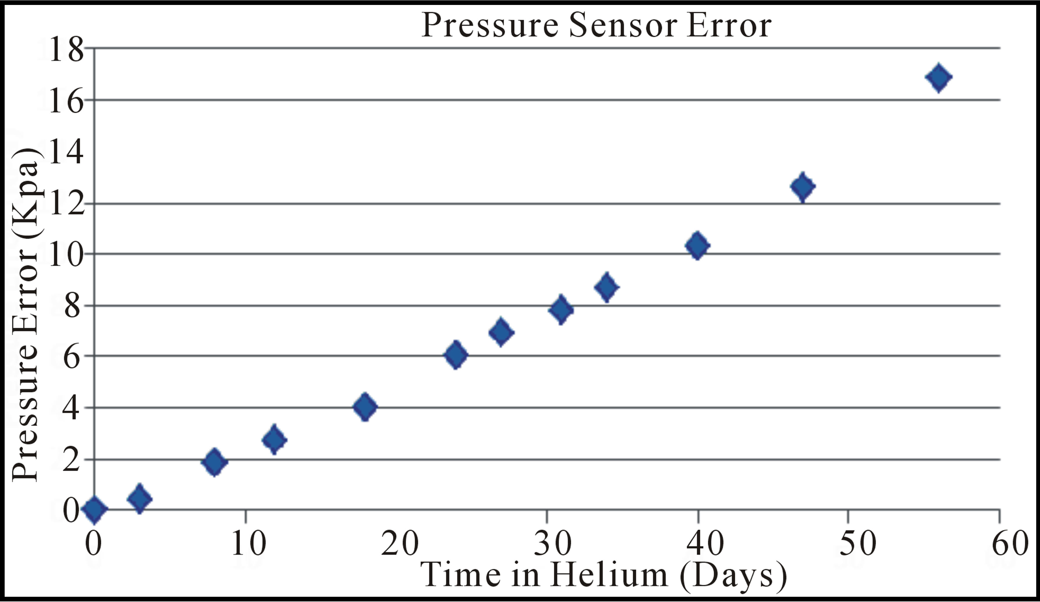
Figure 11. The Freescale pressure sensor error due to 415 KPa helium immersion at room temperature.
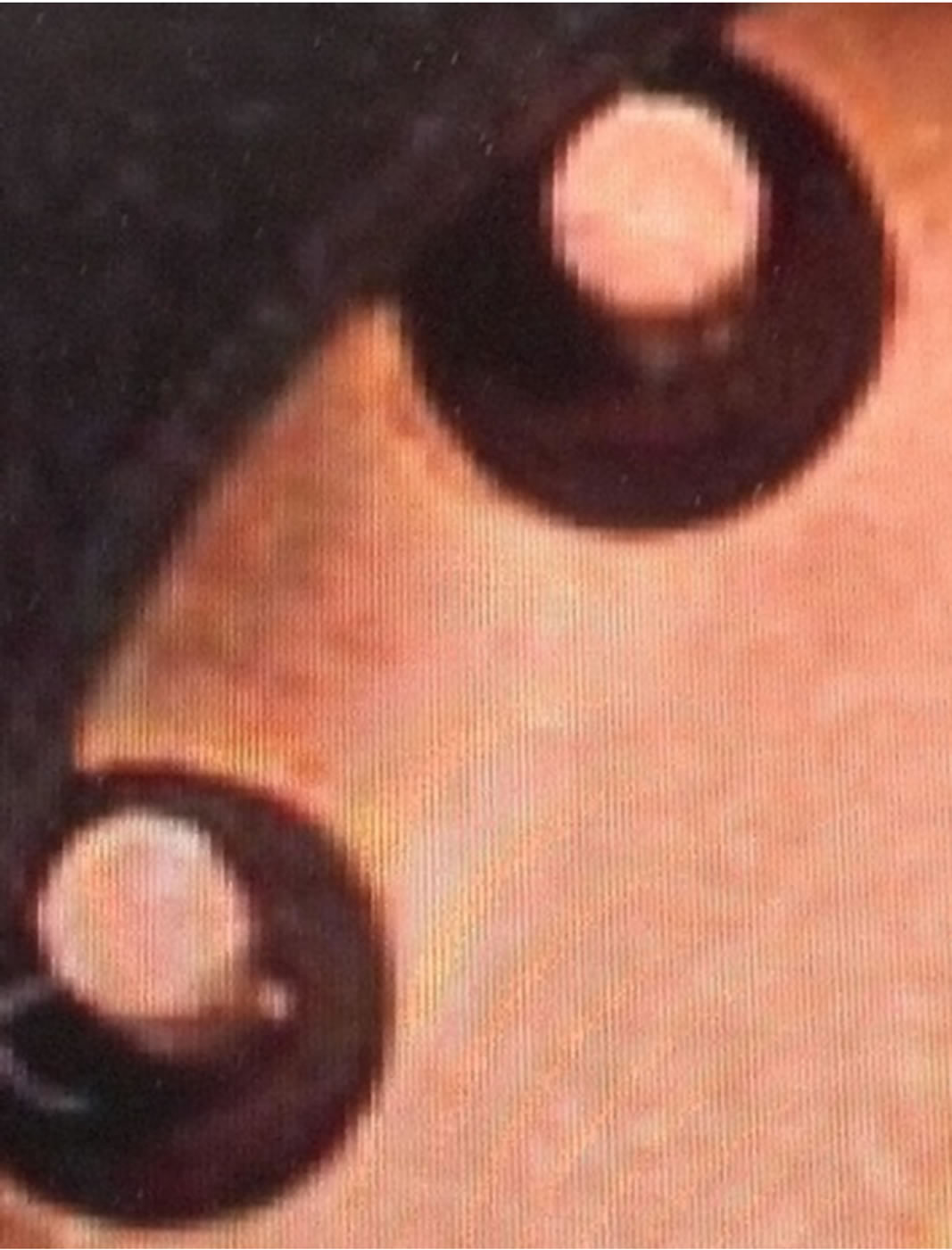
Figure 12. The glass feedthroughs of the metal TO package.
effect was found for differential pressure sensors and pirani gauges vacuum packaged with ceramic or metal packages. The observed results apply to other MEMS devices such as gyroscopes, voltage controlled oscillators, infrared and Coriolis mass flow sensors. Further research and development is needed to investigate the effusion or diffusion of helium in silicon, glass and germanium microstructures in order to develop a chip-scale MEMS vacuum package that can be used in helium or helium gas mixtures.
REFERENCES
- P. Enoksson, G. Stemme and E. Stemme, “A Silicon Resonant Sensor Structure for Coriolis Mass-Flow Measurements,” Journal of MEMS, Vol. 6, 1997, pp. 119-125. http://dx.doi.org/10.1109/84.585789
- R. Smith, D. Sparks, D. Riley and N. Najafi, “A MEMSBased Coriolis Mass Flow Sensor for Industrial Applications,” IEEE Transactions on Industrial Electronics, Vol. 56, No. 4, 2009, pp. 1066-1071. http://dx.doi.org/10.1109/TIE.2008.926703
- H. Toda and T. Kobayakawa, “High-Speed Gas Concentration Measurement Using Ultrasound,” Sensors and Actuators A, Vol. 144, 2008, pp. 1-6. http://dx.doi.org/10.1016/j.sna.2007.12.025
- D. Sparks R. Smith, J. Patel and N. Najafi, “A MEMSBased Low Pressure, Light Gas Density and Binary Concentration Sensor,” Sensors & Actuators A, Vol. 171, 2011, pp. 159-162. http://dx.doi.org/10.1016/j.sna.2011.08.011
- J. Gragg, “Silicon Pressure Sensor,” US Patent 4317126, 1982.
- H. Henmi, S. Shoji, Y. Shoji, K. Yoshimi and M. Esashi, “Vacuum Packaging for Microsensors by Glass-Silicon Anodic Bonding,” Sensors and Actuators A, Vol. 43, 1994, pp. 243-250. http://dx.doi.org/10.1016/0924-4247(94)80003-0
- H. Elgamel, “Closed-Form Expressions for the Relationships between Stress, Diaphragm Deflection, and Resistance Change with Pressure in Silicon Piezoresistive Pressure Sensors,” Sensors and Actuators A, Vol. 50, 1995, pp. 17-12. http://dx.doi.org/10.1016/0924-4247(95)01037-2
- W. Baney, D. Chilcott, X. Huang, S. Long, J. Siekkinen, D. Sparks and S. Staller, “A Comparison between Micromachined Piezoresistive and Capacitive Pressure Sensors, Proceedings of the Fall SAE Conference, 1997, pp. 61- 66.
- B. Kim, R. Candler, R. Melamud, M. Hopcraft, S. Yoneoka, H. Lee, M. Agarwal, S. Chanorkar, G. Yama and T. Kenny, “Hermeticity and Diffusion Investigation in Polysilicon Film Encapsulation for MEMS,” Journal of Applied Physics, Vol. 105, 2009, Article ID: 013514. http://dx.doi.org/10.1063/1.3054366
- D. Sparks, “The Hermeticity of Sealed Microstructures under Low Temperature Helium and Hydrogen Exposure,” Journal of Micromechanics and Microengineering, Vol. 23, 2013, Article ID: 015016. http://dx.doi.org/10.1088/0960-1317/23/1/015016
- D. Sparks, K. Kawaguchi, M. Yasuda, D. Riley, V. Cruz, N. Tran, A. Chimbayo and N. Najafi, “Embedded MEMSBased Concentration Sensor for Fuel Cell and Biofuel Applications,” Sensors and Actuators A, Vol. 145-146, 2008, pp. 9-13. http://dx.doi.org/10.1016/j.sna.2007.10.015
- J. Mitchell, G. Lahiji and K. Najafi, “An Improved Performance Poly-Si Pirani Vacuum Gauge Using Heat-Distributed Structural Supports,” Journal of MEMS, Vol. 17, 2008, pp. 93-102. http://dx.doi.org/10.1109/JMEMS.2007.912711
- J. Mitchell and K. Najafi, “A Detailed Study of Yield and Reliability for Vacuum Packages Fabricated in a WaferLevel Au-Si Eutectic Bonding Process,” Denver, Transducers, 2009, Article ID: T2E.004.
- D. Sparks, S. Massoud-Ansari and N. Najafi, “Long-Term Evaluation of Hermetically Glass Frit Sealed Silicon to Pyrex Wafers with Feedthroughs,” Journal of Micromechanics and Microengineering, Vol. 15, 2005, pp. 1560- 1564. http://dx.doi.org/10.1088/0960-1317/15/8/026
- H. Cady and D. McFarland, “Helium in Natural Gas,” Science, Vol. 24, 1906, pp. 344-347. http://dx.doi.org/10.1126/science.24.611.344
- S. García-Blanco, P. Topart, Y. Desroches, J. Caron, F. Williamson, C. Alain and H. Jerominek, “Low Temperature Hermetic Wafer-Level Package for Uncooled Microbolometer FPAs,” Proceedings of SPIE 6884, 2008, Article ID: 68840P-1.
- D. Sparks, G. Queen, R. Weston, G. Woodward, M. Putty, L. Jordan, S. Zarabadi and K. Jayakar, “Wafer-to-Wafer Bonding of Nonplanarized MEMS Surfaces Using Solder,” Journal of Micromechanics and Microengineering, Vol. 11, No. 6, 2011, pp. 630-634. http://dx.doi.org/10.1088/0960-1317/11/6/303
- J. Vinti, “The Dispersion and Absorption of Helium,” Physical Reviews, Vol. 42, 1932, pp. 632-640. http://dx.doi.org/10.1103/PhysRev.42.632
- R. Osiander and A. Darrin, “MEMS for Automotive and Aerospace Applications,” Woodhead Publishing, Oxford, 2013, p. 324.
- Y. Tao and A. Malsha, “Theoretical Investigation on Hermeticity Testing of MEMS Packages Based on MILSTD-883E,” Microelectronics and Reliability, Vol. 45, 2005, pp. 559-566. http://dx.doi.org/10.1016/j.microrel.2004.08.004
- T. Anthony, “Anodic Bonding of Imperfect Surfaces,” Journal of Applied Physics, Vol. 58, No. 5, 1983, pp. 2419-2424. http://dx.doi.org/10.1063/1.332357
- Q.-Y. Tong and U. Gösele, “Semiconductor Wafer Bonding: Science and Technology,” Wiley Interscience, New York, 1999.
- R. Swanson, “Electronic Pressure Transmitters: The Hydrogen Problem,” Sensors, Vol. 10, 1993, pp. 33-40.