Advances in Chemical Engineering and Science
Vol.4 No.4(2014), Article
ID:49786,7
pages
DOI:10.4236/aces.2014.44042
Room Temperature and Reduced Pressure Chemical Vapor Deposition of Silicon Carbide on Various Materials Surface
Hitoshi Habuka*, Asumi Hirooka, Kohei Shioda, Masaki Tsuji
Department of Chemical and Energy Engineering, Yokohama National University, Yokohama, Japan
Email: *habuka1@ynu.ac.jp
Copyright © 2014 by authors and Scientific Research Publishing Inc.
This work is licensed under the Creative Commons Attribution International License (CC BY).
http://creativecommons.org/licenses/by/4.0/


Received 20 August 2014; revised 31 August 2014; accepted 10 September 2014
ABSTRACT
At room temperature, 300 K, silicon carbide film was formed using monomethylsilane gas on the reactive surface prepared using argon plasma. Entire process was performed at reduced pressure of 10 Pa in the argon plasma etcher, without a substrate transfer operation. By this process, the several-nanometer-thick amorphous thin film containing silicon-carbon bonds was obtained on various substrates, such as semiconductor silicon, aluminum and stainless steel. It is concluded that the room temperature silicon carbide thin film formation is possible even at significantly low pressure, when the substrate surface is reactive.
Keywords:Silicon Carbide, Monomethylsilane, Chemical Vapor Deposition, Room Temperature, Reduce Pressure

1. Introduction
Silicon carbide (SiC) is a suitable coating material for protecting various materials surface from a harsh and high-temperature environment [1] , because of its chemical and mechanical stability. One of the well-known applications is the carbon susceptor surface coating film for a chemical vapor deposition (CVD) reactor. The CVD reactor very often uses hydrogen chloride gas at high concentrations and high temperatures for the reactor cleaning [2] . Such the suitable nature should be applied extensively for coating various kinds of materials having high and low melting points. However, because the ordinary temperature for silicon carbide film formation by the CVD [3] -[5] is very often higher than the melting points of many useful metals, an alternative CVD technique possible at low temperatures is necessary. Thus, the room temperature technique has been developed using monomethylsilane (MMS) gas [6] .
The room temperature silicon carbide CVD process [6] consisted of the two room-temperature steps, that is, (A) the reactive surface preparation using argon plasma etching, and (B) the silicon carbide film formation from monomethylsilane gas. The atmospheric pressure has been used for the film deposition in order to supply the monomethylsilane gas at the significantly high concentrations, often 100%. By this technique, the silicon carbide film could be formed at the surface of semiconductor silicon and the aluminum. But it accompanied slight oxidation at the interface between the substrate and the silicon carbide film. Because the previously-used process had the substrate transfer operation from the plasma etcher to the CVD reactor via air ambient, the reactive sites, such as dangling bonds produced by the argon plasma etching, might become inactive by oxidation.
In order to effectively maintain the reactive sites, the entire process should be performed without exposure to air, by means of deleting a substrate transfer operation. The easiest way is to introduce the monomethylsilane gas into the chamber of plasma etcher. In such the condition, the partial pressure of monomethylsilane gas must become significantly lower than that by the atmospheric pressure process [6] , because the reduced pressure is necessary for assuring the safety operation. Thus, the possibility of room temperature film formation at such the reduced pressure should be experimentally evaluated.
In this study, the silicon carbide film formation process was developed for the surface of various materials, such as semiconductor silicon, aluminum and stainless steel. The entire process was performed at room temperature and reduced pressure.
2. Experimental Procedures
The surface chemical process designed in this study is shown in Figure 1. The substrate surface is usually oxidized and has an airborne contamination, as shown in Figure 1(a). The argon plasma physically removes the atoms of the material surface to produce the dangling bonds, as shown in Figure 1(b). The dangling bonds capture the monomethylsilane molecule, as shown in Figure 1(c). Figure 1(d) shows that the silicon-carbon pair remains on the substrate surface after the hydrogen desorption.
The substrates used in this study were the plates of silicon, aluminum and stainless steel (SUS430). The silicon plate was cut from the 200 mm-diameter (100) semiconductor silicon wafer. The aluminum and stainless steel plates used in this study were low cost materials manufactured for a handicraft use. Because they have been exposed to air for sufficiently long period, their surfaces were covered with a native oxide film. The substrates having the dimensions of 10 mm wide and 10 mm long were cut from these plates and were cleaned by ethanol
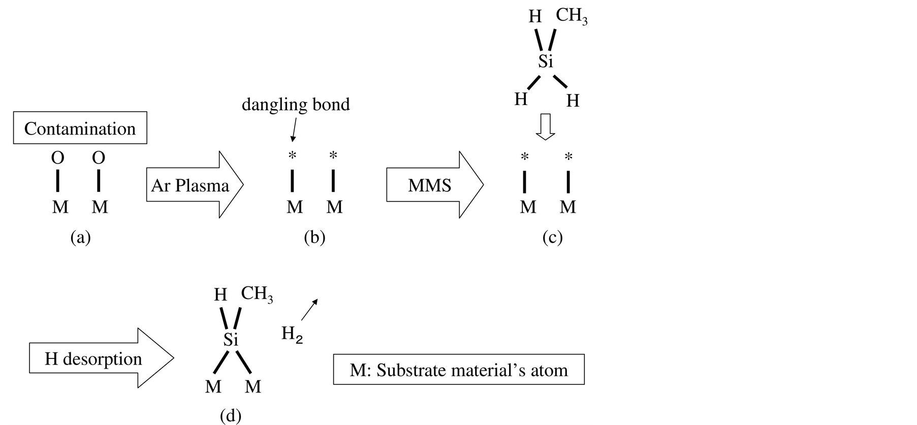
Figure 1. Steps for silicon carbide film deposition. Step (A): dangling bond formation using argon plasma at 10 Pa for 20 min at room temperature; Step (B): silicon carbide film formation at room temperature using monomethylsilane gas at 1% and 10 Pa for 10 min.
without any additional wet cleaning.
The reactive substrate surface was prepared by argon plasma etching, following the mechanism shown in Figure 2. This process consisted of Steps (A) and (B), as shown in Figure 2. Step (A) is the plasma etching using a parallel plate plasma etcher (Soft Plasma Etcher-SE, Meiwafosis Co., Ltd., Tokyo, Japan). Step (A) prepared the reactive surface by the etching for 20 min in argon plasma at 10 Pa and room temperature without any additional heating. After Step (A), the pressure was decreased to less than 1 Pa in order to reduce unnecessary gas species. Next, in Step (B), the substrate was exposed to monomethylsilane gas, the concentration of which was 1%, at 10 Pa for 10 min at room temperature without any plasma assistance. The partial pressure of monomethylsilane gas was 0.1 Pa. The monomethylsilane concentration of 1% proves the safety operation because it was less than the flammable lowest limit in air, that is, 1.3% [7] . In this study, the substrates could be prevented from the oxidation, because of no exposure to air achieved by no transfer operation.
The surface morphology was evaluated using a scanning electron microscope (SEM) (VE-8800, Keyence, Tokyo). In order to obtain information about the chemical bonds in the very thin film formed on the substrate surface, a Time-of-Flight Secondary Ion Mass Spectrometer (ToF-SIMS) (TOF-SIMS300, ION-TOF GmbH, Munster, Germany) was used. The ToF-SIMS was ex situ performed at the Foundation of Promotion of Material Science and Technology of Japan (Tokyo). The ToF-SIMS profiles obtained in this study were compared with those by the previous study [6] .
3. Results and Discussion
3.1. Film Formation on Silicon Surface
Figure 3 shows the depth profiles of SiC, SiC2, C3, C6, Si4 and Si2O5 in the film obtained on silicon substrate. These profiles were measured by ToF-SIMS. Figure 3(a) shows the silicon carbide film formed at atmospheric pressure accompanying the substrate transfer operation in air ambient [6] . In the region from the surface to 5 nm depth, SiC and SiC2 were detected at very high concentrations. These profiles showed the existence of silicon carbide film. Simultaneously, the C3 concentration was very high; its profile resembled to those of SiC and SiC2. In contrast, the Si4 concentration increased with the increasing depth, particularly from the surface to the 5 nm depth. The SiC, SiC2, C3 and Si4 profiles indicates that the layer switched from silicon to silicon carbide at the position near 5 nm depth. This conclusion was consistent with the Si2O5 profile. The Si2O5 profile had two peaks at the surface and 5nm depth. The former shows the oxidation of the intermediate species of monomethylsilane remained at the obtained film surface. The latter indicates the oxidation of silicon substrate surface due to the exposure to air ambient during the substrate transfer from the plasma etcher to the CVD reactor. Thus, the all profiles in Figure 3(a) indicate the existence of 5-nm-thick silicon carbide film at the silicon substrate surface.
Figure 3(b) is the SiC2, C3, C6, Si2O5 and Si4 depth profiles of the film obtained at reduced pressure without
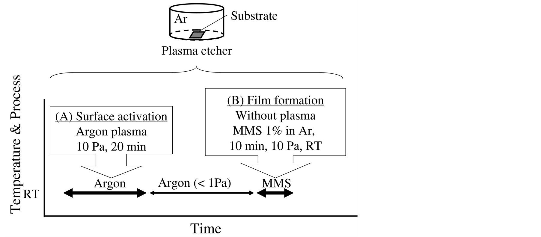
Figure 2. Silicon carbide film deposition process linked with the reactive surface preparation by means of the argon plasma etching.
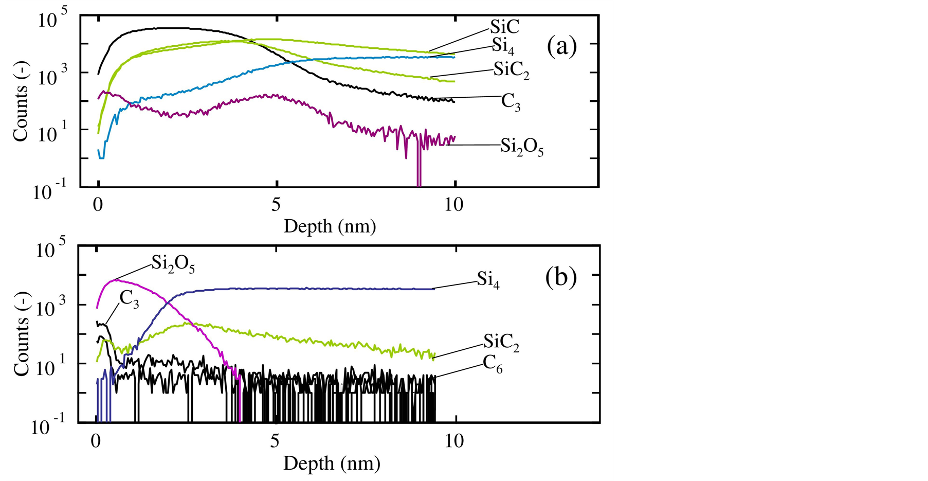
Figure 3. Depth profiles of SiC, SiC2, C3, C6, Si4 and Si2O5 in the film obtained on silicon substrates, measured by ToF-SIMS. The CVD process was performed (a) with and (b) without a substrate transfer operation in air ambient.
the substrate transfer. This figure shows the broad peak of SiC2 at the depth around 3 nm. The Si2O5 was formed at the film surface similar to Figure 3(a), because of the oxidation of the remained intermediate species of monomethylsilane. The Si2O5 decreased from 0.5 nm to 4 nm depth, while SiC2 increased and showed a peak in the same region. Additionally, Si4 significantly increased from the surface to the region near 3 nm. These profiles indicate that there existed three layers from the top surface, such as silicon oxide, silicon carbide and silicon. Additionally, at the interface between the silicon carbide film and the silicon substrate surface, there was no or quite less silicon oxide. At least, the interface had no silicon oxide peak.
In Figure 3(b), the profiles of C3 and C6 was localized near the surface, such as in the region shallower than 0.5 nm depth, while those in Figure 3(a) distributed over the silicon carbide film. Thus, the process without the substrate transfer could produce the silicon carbide film with the low concentration of carbon-carbon bonds.
Because the obtained films were very thin, that is, several nm thick, the silicon substrate surface before and after the film formation showed similarly mirror appearance, by the SEM.
3.2. Aluminum Surface
Figure 4(a-1) and Figure 4(a-2) show the aluminum substrate surface morphology before and after the film formation, respectively, observed by the SEM. Figure 4(a-1) showed that there were many scratches in a horizontal direction, with some small round-shaped pits having a diameter of less than 10 μm. After the film formation, there were many sharp linear scratches in a horizontal direction, as shown in Figure 4(a-2). Some scratches were jig-sag shaped. The surface appearance had no obvious difference from Figure 4(a-1).
Figure 5 shows the depth profiles of SiC2, C3, C6, Al4 and Al2O3 in the film obtained on aluminum substrates. Figure 5(a) shows the silicon carbide film formed accompanying the substrate transfer operation in air ambient [6] . There was a broad peak of SiC2 in the range from the surface to 5 nm depth. The C3 peak was observed at about 1 nm depth, at which the concentration of Si2O5 were slightly large. This is considered to be produced by the oxidation of monomethylsilane intermediate species. Although the concentration of Al2O3 was entirely large, it tended to decrease with approaching the film surface in a range shallower than 1 nm. The information in Figure 5(a) entirely indicated that the silicon-carbon bonds existed in the obtained film in the range from the surface to 5 nm depth.
Figure 5(b) is the depth profile of SiC2, C3, C6, Al4 and Al2O3 in the silicon carbide film obtained in this study. This figure shows the existence of SiC2 in the range from the surface to the depth of 5 nm accompanying
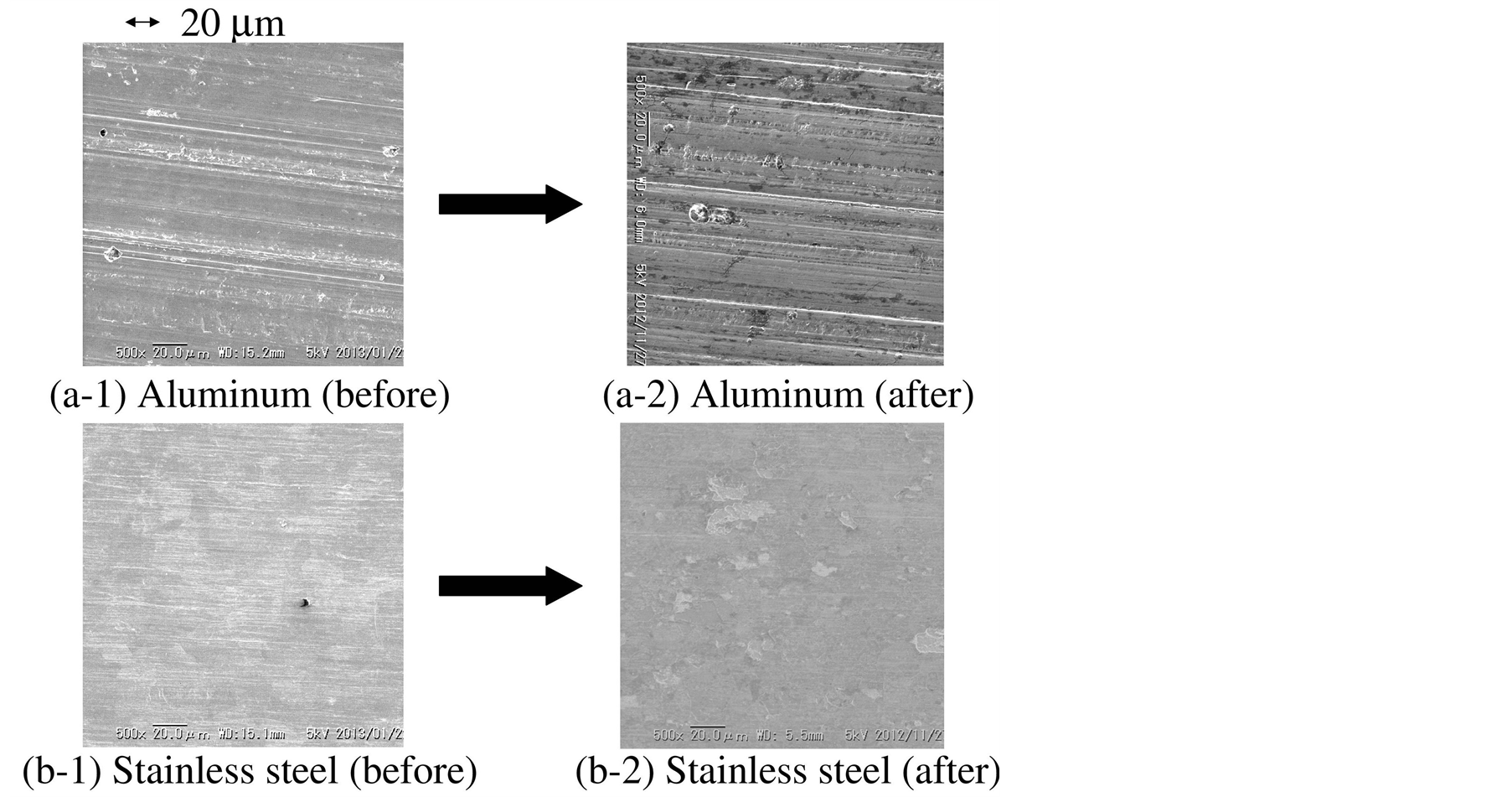
Figure 4. SEM image of aluminum substrate surface (a-1) before and (a-2) after the deposition. That of stainless steel substrate surface (b-1) before and (b-2) after the deposition.
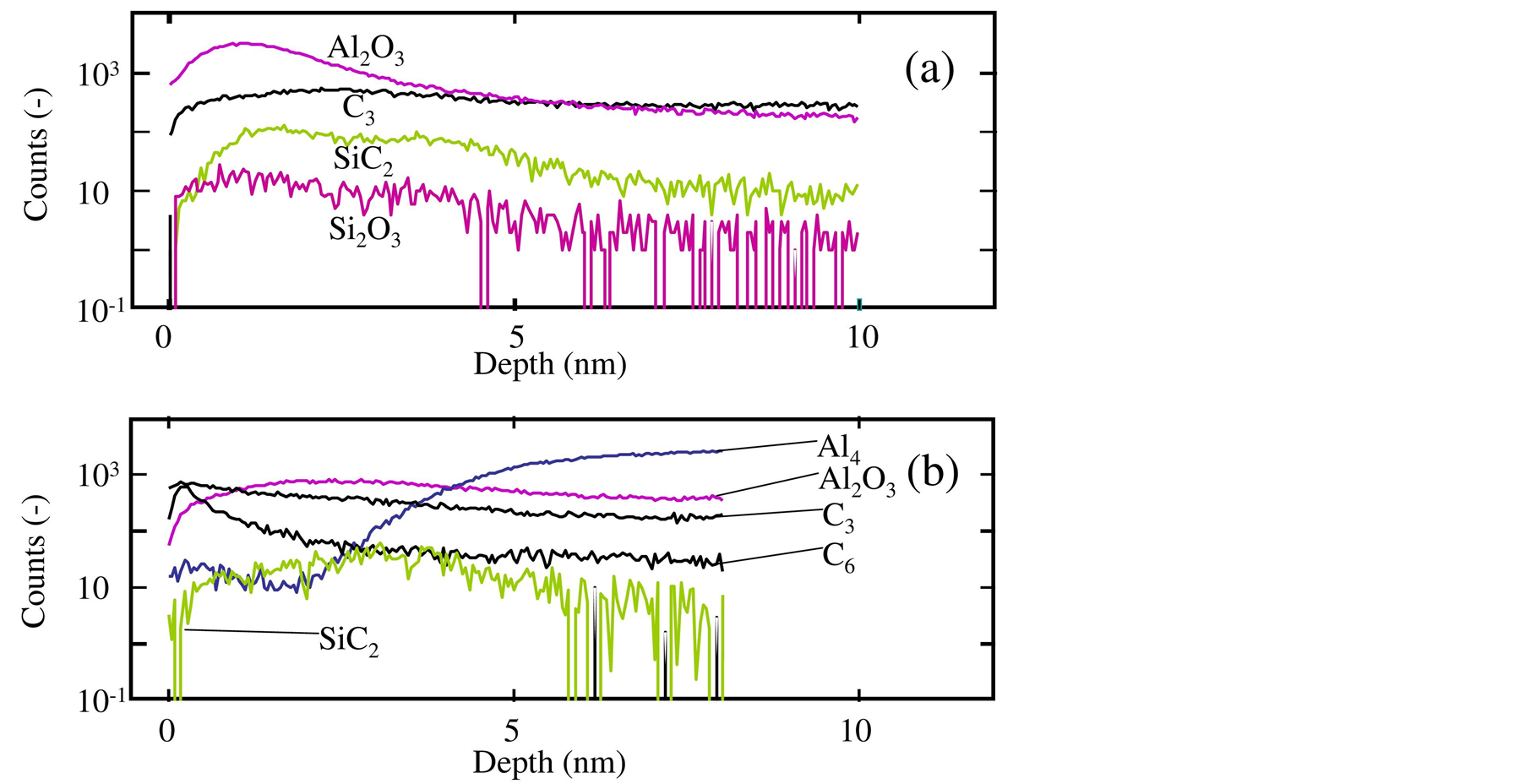
Figure 5. Depth profiles of SiC, SiC2, C3, C6, Al4 and Al2O3 in the film obtained on aluminum substrates, measured by ToF-SIMS. The CVD process was performed (a) with and (b) without a substrate transfer operation in air ambient.
a broad peak near 3 nm. Consistently, the Al4 concentration significantly increased from 3 nm to 6 nm depth, indicating the existence of bulk aluminum. Because the Al2O3 widely distributed, a considerable amount of aluminum oxide remained after the plasma etching. This figure simultaneously showed that the C3 and C6 widely distributed. Because the aluminum surface initially had no carbon film before the film formation, these profiles also indicated that the chemical reaction of monomethylsilane gas could occur.
In order to further evaluate the film formation and the crystalline quality, the high resolution TEM image was taken, as shown in Figure 6, which was the silicon carbide film formed on the aluminum substrate surface. Each dot in this figure showed an atom; the dark contrast layer at the mid height of this figure showed the interface between the substrate and the obtained film. The lower layer in this figure showed aluminum substrate; the upper layer was silicon carbide. The thickness of silicon carbide layer was about 5 nm, which agreed with the ToF-SIMS profile shown in Figure 5(b). Because the dot pattern in the upper layer was not periodically, the obtained silicon carbide film was determined to be amorphous.
3.3. Stainless Steel Surface
Figure 4(b-1) and Figure 4(b-2) show the surface morphology of the stainless steel substrate surface before and after the deposition, respectively. Figure 4(b-1) showed that there were many shallow and thin scratches in a horizontal direction before the film formation. After the film formation, the surface still had many shallow scratches, as shown in Figure 4(b-1). Entirely, the surface morphology did not have obvious change by the film formation.
Figure 7 shows the depth profiles of SiC2, Si2O3, C3, C6, Fe2 and FeO2 in the film obtained on stainless steel substrates. Figure 7(a) shows the SiC2, Si2O3, C3 and FeO2 profiles from the surface after the film formation
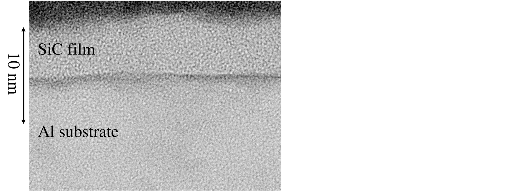
Figure 6. Cross sectional TEM image of silicon carbide film formed on aluminum substrate. Upper layer is amorphous silicon carbide; lower layer is aluminum oxide.
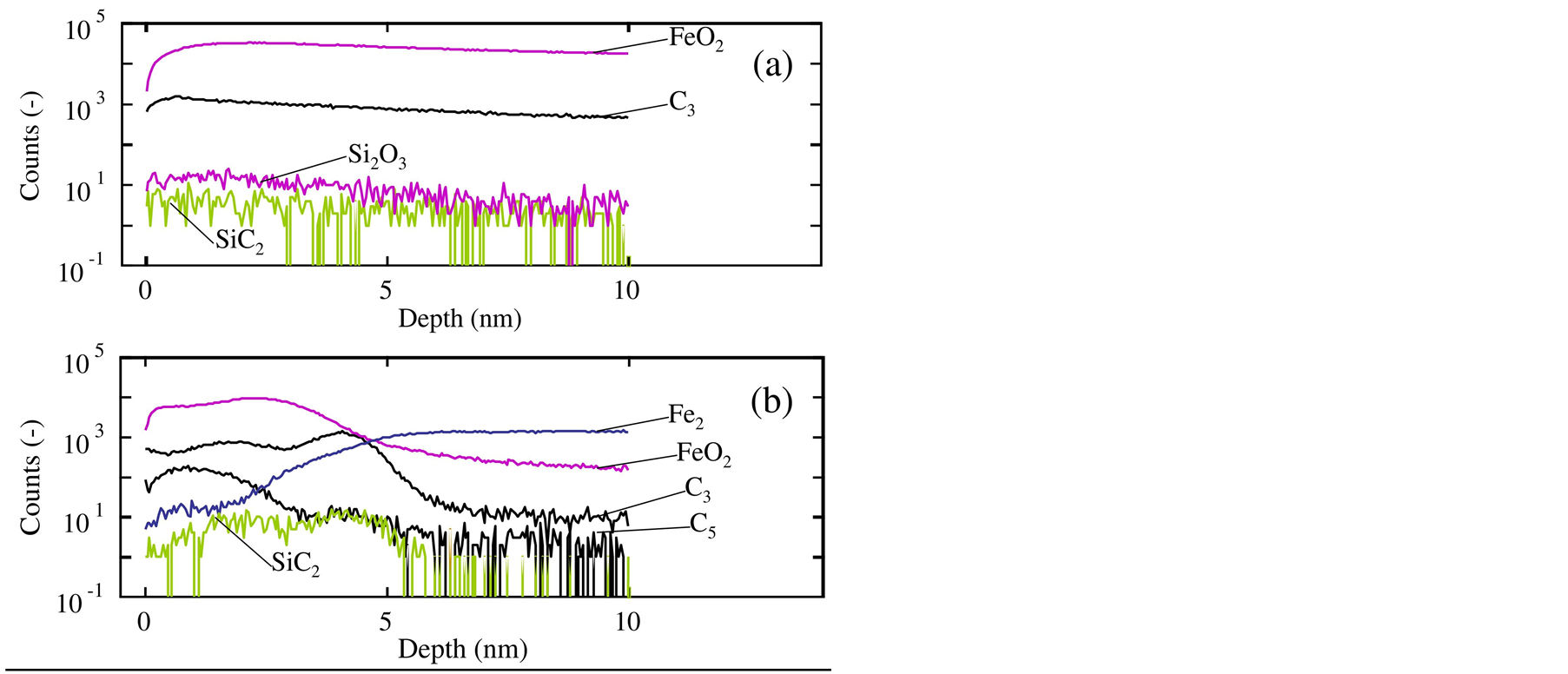
Figure 7. Depth profiles of SiC, SiC2, C3, C6, Al4 and Al2O3 in the film obtained on stainless steel substrates, measured by ToF-SIMS. The CVD process was performed (a) with and (b) without a substrate transfer operation in air ambient.
accompanying the substrate transfer operation in air ambient [6] . In this figure, only very small C3 peak existed very near the surface. The Si2O3 concentration in a range shallower than 3 nm was very slightly larger than that in a deep position; the C3 and Si2O3 existed at the stainless steel surface. However, the SiC2 concentration was unfortunately and significantly low and flat from the surface to the deep position. This concluded that the recognizable amount of silicon-carbon bond did not remain at the stainless steel substrate surface.
Figure 7(b) is the depth profile of SiC2, C3, C5, Fe2 and FeO2 in the film obtained without an exposure to air. This figure shows the existence of SiC2 from the surface to the depth of 5 nm. Although the amount of SiC2 in this range was not significant, it was larger than that in the deep position such as at 10 nm, and was rather flat from 2 nm to 5 nm depth. The low concentration might indicate that the coverage by the silicon carbide was partial. In this range, the Fe2 concentration became larger, while the FeO2 decreased. Thus, the stainless steel substrate surface had about 3 - 4 nm-thick iron oxide film. This figure simultaneously showed that C3 and C5 peaks existed at the depth of 4 nm and 1 nm, respectively.
From the profiles of SiC2, C3 and C5, the silicon-carbon bonds were concluded to be formed at the stainless steel surface. However, Figure 7(b) showed the entire coexistence of silicon carbide and iron oxide in the film. Because the stainless steel substrate surface was not completely covered with the silicon carbide film, the substrate surface was partially oxidized after the film formation till the ToF-SIMS measurement.
Entirely, the silicon-carbon bond concentration was significantly low. This will be able to be increased by increasing the monomethylsilane partial pressure for the film formation.
4. Conclusions
Silicon carbide thin film formation at room temperature and reduced pressure was performed on three kinds of substrates, such as semiconductor silicon, aluminum and stainless steel, using monomethylsilane gas. First, the reactive surface having dangling bonds was prepared by means of the argon plasma etching at room temperature. Next, the silicon carbide thin film was formed at room temperature and reduced pressure using monomethylsilane gas without exposing the substrate surface to air. Because the silicon-carbon bonds were detected in the several nanometer-thick films, the silicon carbide thin film could be formed on various materials surface even at the significantly low concentration of monomethylsilane gas.
References
- Greenwood, N.N. and Earnshaw, A. (1997) Chemistry of the Elements. 2nd Edition, Butterworth-Heinemann, Oxford.
- Rinaldi, A.M. and Crippa, D. (2001) Silicon Epitaxy. In: Crippa, D., Rode, D.L. and Masi, M., Eds., Academic Press, San Diego.
- Kimoto, T. and Matsunami, H. (1994) Surface Kinetics of Adatoms in Vapor Phase Epitaxial Growth of SiC on 6H-SiC{0001}Vicinal Surfaces. Journal of Applied Physics, 75, 850-859.
http://dx.doi.org/+10.1063/1.356439 - Myers, R.L., Shishkin, Y., Kordina, O. and Saddow, S.E. (2005) High Growth Rates (>30 μm/h) of 4H-SiC Epitaxial Layers Using a Horizontal Hot-Wall CVD Reactor. Journal of Crystal Growth, 285, 486-490. http://dx.doi.org/10.1016/j.jcrysgro.2005.09.037
- Kotamraju, S., Krishnan, B., Melnychuk, G. and Koshka, Y. (2010) Low-Temperature Homoepitaxial Growth of 4H-SiC with CH3Cl and SiCl4 Precursors. Journal of Crystal Growth, 312, 645-650. http://dx.doi.org/10.1016/j.jcrysgro.2009.12.017
- Habuka, H. and Tsuji, M. (2013) Amorphous Silicon Carbide Chemical Vapor Deposition on Metal Surface Using Monomethylsilane Gas at Low Temperatures. Surface and Coatings Technology, 217, 88-93. http://dx.doi.org/10.1016/j.surfcoat.2012.11.078
- Praxair Material Safety Data Sheet, MSDS Plaxair, December 2009.
NOTES

*Corresponding author.