Graphene
Vol.3 No.3(2014), Article
ID:48096,11
pages
DOI:10.4236/graphene.2014.33005
Transferring Few-Layer Graphene Sheets on Hexagonal Boron Nitride Substrates for Fabrication of Graphene Devices
J. A. Leon1*, N. C. Mamani2, A. Rahim1, L. E. Gomez3, M. A. P. da Silva2,4, G. M. Gusev1
1Departamento de Física dos Materiais e Mecânica, Instituto de Física da Universidade de São Paulo, São Paulo, Brazil
2Instituto de Física de São Carlos, Universidade de São Paulo, São Carlos, Brazil
3Grupo de Óptica, Micro e Nanofabricação de Dispositivos (GOMNDI), Universidade Federal do Pampa, Rio Grande do Sul, Brazil
4Centro Universitário Central Paulista (UNICEP), São Carlos, Brazil
Email: *jleoner@gmail.com
Copyright © 2014 by authors and Scientific Research Publishing Inc.
This work is licensed under the Creative Commons Attribution International License (CC BY).
http://creativecommons.org/licenses/by/4.0/


Received 11 April 2014; revised 20 May 2014; accepted 27 June 2014
ABSTRACT
We have developed a dry transfer method that allows graphene to be transferred from polymerthyl-methacrylate (PMMA)/Si (silicon) substrates on commercially available hexagonal boron nitride (hBN) crystals. With this method we are able to fabricate graphene devices with little wrinkles and bubbles in graphene sheets, but that do not degrade the electronic quality more than the SiO2 substrate does. For hBN to perform the function described above substrate cleanliness is critical to get high quality graphene devices. Using hBN as a substrate, graphene exhibits enhanced mobility, reduced carrier inhomogeneity, and reduced intrinsic doping compared to graphene on SiO2 substrate.
Keywords:Graphene, Boron Nitride, Transfer Method, Raman Spectroscopy

1. Introduction
The search for new substrates that improve graphene properties has been an intense focus of research since graphene was first isolate in 2004 [1] . In the case of SiO2, the most commonly used substrate for graphene devices, it has been shown that the presence of trapped charges [2] , roughness [3] and surface phonons [4] limits the mobility of charge carries in devices. These impurity-induced charge traps tend to cause the graphene to electronically break up into electron-and hole doped regions at low charge density, which both limit device performance and make the Dirac point physics inaccessible [5] . Suspension of graphene membranes has been successfully used to remove the unwanted effects of SiO2 substrates and mobilities as high as 230,000 cm2∙V−1∙s−1 at charge carrier densities of n = 2 ´ 1011 cm−2 and T = 4 K has been obtained this way [6] [7] . However, the freely-suspended monolayers are very delicate, leading to fabrication difficulties and making impossible to access high carrier densities in suspended devices as well as strain [8] . Therefore alternative substrates are required to overcome these limitations.
The quality of substrate-supported graphene devices has not improved since the first observation of the anomalous quantum Hall effect in graphene and its bilayer [9] [10] . Recently, hexagonal boron nitride (hBN) has received a great deal attention as a substrate material for high performance graphene electronic [11] because it has an atomically smooth surface, lattice constant similar to that of graphene, large optical phonon modes, and a large electrical band gap. Using hBN as a substrate, graphene exhibits reduced carrier inhomogeneity, reduce intrinsic doping compared to graphene [12] , and enhanced mobilities of 140,000 cm2∙V−1∙s−1 near the charge neutrality point. It has been demonstrated by scanning tunneling microscopy that graphene on hBN significantly reduce electron-hole puddles as compared to SiO2 [13] . Furthermore, by reducing the charge fluctuations, the low density regime and the Dirac point can be more readily accessed. Consequently new physics was found such as fractional quantum hall states [14] , broken SU(4) symmetry at very low fields [15] in single layer graphene, unconventional quantum Hall effect in tri-layer graphene [16] , and ballistic transport at room temperature [17] .
In this work, we address a mechanical transfer method to deposit graphene on boron nitride substrates in order to fabricate graphene based devices. The hBN crystals were commercially available (Momentive, Polarthem grade PT110) that are smaller size of order of ~45 µm than non-commercial ultrapure hBN. Different manners of exfoliation of both hBN and graphene were developed, aiming to optimize the best way of exfoliation. Finally we will characterize the graphene transferred using Raman microscopy, atomic force microscopy and electronic transport measurements in fabricated graphene devices.
2. Experimental
We first deposit thin hBN crystals (Momentive, Polartherm grade PT110) on a Si wafer with 285 nm of SiO2 by mechanical exfoliation of hBN powder using a Blue Medium Tape P/N 18074 (Semiconductor Equipment Corp.) keeping the substrate and tape for 4 minute. By optical microscopy few layer hBN flakes were initially identified. The surface of every hBN flake is characterized by atomic force microscopy (AFM) (BRUCKER-Icon) to ensure it is free of contaminants or step edges, and also to measure its thickness. Number of layers in a hBN flake can be confirmed by measuring their thickness. Since 0.35 nm is the lattice constant for hBN in C direction, therefore, AFM may be useful for this purpose. It has been deduced from AFM images that a thickness of 20 - 30 nm corresponds to light blue flakes of hBN, as shown in Figure 1(a). After exfoliating the hBN, the samples were annealed using a ~1 inch quartz tube furnace (Linderg Blue M) to remove any excess tape residue. Gas pressure was kept at ambient, and gas flow rate were 500 sccm Ar and 50 sccm O2. The temperature is set to 500˚C with an up-rate of 7˚C/min and typically thermal annealing lasted 2 - 3 h [18] . Graphene is exfoliated separately onto a Si substrate coated with a polymer bi-layer consisting of a water-soluble layer (Polyvinyl alcohol) PVA and PMMA using the Scotch Magic tape. We first spin PVA at 6000 rpm for 60 s and bake the chip at 160˚C for 5 min. We then spin PMMA 950K A7 on top of PVA at 2400 rpm for 60 s and heat at 160˚C for 5 minutes. The source of materials was natural graphite from National of Graphite (www.grafite.com Brazil). These crystals produce large area of graphene, approximately 30 µm length. We start deposition by sticking a relatively large piece of graphite on the tape (~1.7 mm in diameter). Then we fold the tape and stick it together, followed by slowly tearing the tape apart. We repeat this stick-and-tear process on different areas of the tape and thereby we spread the graphite over its surface. We continue until the peace of tape is covered with graphite. Then we stick the tape to the target substrate, rub it with a light plastic object and wait for 4 minute before removing from the substrate by simple peeling it back. After exfoliation, the graphene flake is identified using an optical microscope. Different optical filters were used in the microscope to enhanced the visibility of graphene on the substrate [19] . For this particular sample, the red filter (620 nm) gave maximum contrast. Raman spectroscopy has been used to identify and select individual single layer, bilayer and few-layer graphene that is
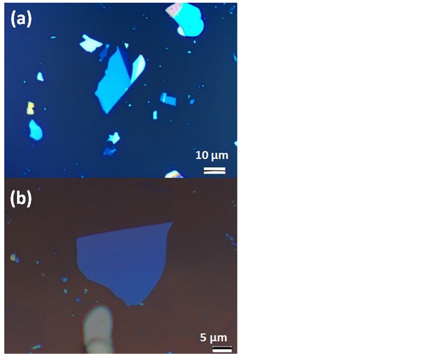
Figure 1. (Color online) Optical image of two suitable hBN flakes exfoliated on Si/SiO2 substrate with thickness of (a) ≈22 nm and (b) ≈13 nm.
deposited on bi-layer PVA/PMMA. The Raman data are recorded by using a micro-Raman spectrometer (Renishaw InVia) setup with a laser excitation of 632.8 nm (EL = 1.96 eV), using a 100´ objective, with a laser spot size ≈ 1 µm. We used a laser power about 10 mW such that heating effects can be neglected [20] .
A crucial breakthrough in this paper is the development of a special method to transfer graphene from one substrate to an exact location on another substrate (in this case an hBN flake). In this method extreme care is taken to reduce water residues and this is named “dry transfer method”. We adapted the dry transfer method to our needs. A dry transfer method consists mainly of four steps as illustrated in Figure 2. In step A the PMMA (carrying the graphene) is suspended in a plastic window which has been attached to the chip by using doubleside tape to the PMMA side, illustrated in Figure 2(a). Next in the step B the sacrificial PVA film is dissolved in DI water to release the PMMA film from its substrate. The graphene is on top of the PMMA so it will never be in contact with water. The result is shown in Figure 2(b). In step C we adhered the PMMA membrane to an aluminum transfer slide, which is clamped to mask aligner (Karl Suss MBJ-3) modified. During the transfer process, we fix the hBN containing substrate on the holder (Figure 2(c)). In step D, using the optical mask micro-manipulators, we align the graphene flake to the hBN crystal and lower the polymer side onto the substrate, as shown in Figure 2(d). When the polymer touches the substrate, it makes strong contact with the SiO2 substrate. Then, we turn off the nitrogen valve of the mask aligner and down the holder substrate along with the PMMA polymer attached to it. We finally put the substrate with target hBN flake on a custom made heater that we set to 110˚C to enhance adhesion between graphene and hBN for at least 10 minute. Next the sample is allowed to cool down and the PMMA is removed with acetone and isopropanol (IPA). As chemical cleaning with organic solvents always leaves some residues we anneal the samples as well. At this stage we heat the samples
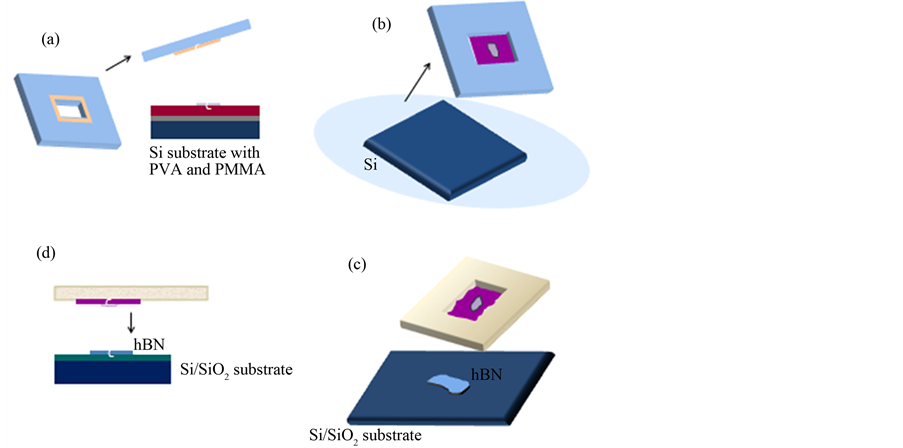
Figure 2. (Color online) Schematic illustration of the dry transfer method to fabricate graphene-on-hBN devices. (a) PVA/PMMA film with graphene is glued in the plastic window; (b) Next the bi-layer is put in water, in order to dissolve the PVA film, releasing the PMMA with graphene from the Si substrate; (c) The plastic window is attached to aluminum slide with a hole and the hBN flake is exfoliated on Si/SiO2; (d) The aluminum slide is mounted to a micromanipulator from a mask aligner that allows us to align graphene with the hBN flake.
slowly to 400˚C in a tube oven (1" Lindberg Blue M) in forming gas environment and anneal them there for ∼3 hours before slowly cooling down to room temperature. This treatment is very effective in removing polymer residues from the transfer.
After transfer process, we fabricate the electronic device using standard beam lithography (Raithe_Plus) and deposit chromium/gold (5 nm/60 nm) contact material using e-gun evaporation system. The polymer mask used for processing was PMMA 950K dissolved in anisole (7%). Lift-off was done in acetone, followed by isopropanol rising.
3. Results and Discussion
3.1. Characterization of Graphene Flakes
We made approximately 40 exfoliations on SiO2/Si substrates and with helping of the optical microscopy, with good resolution; they were observed different sizes and colors. They were chosen flakes of light and dark blue colors and 20 - 40 µm size. These flakes are also thick enough to compensate for the SiO2 roughness, and thin enough to allow good backgate functionally, when are used as electronic devices. After finding suitable flakes AFM, images of the hBN were made to check surface roughness and possible contaminants. Approximately 1 out of 10 flakes have the correct thickness; appear clean and flat under the AFM. The relatively low chance of having a flat and clean flake could possibly explained by the fact that the hBN crystal will likely break at the weak spots in the crystal during mechanical exfoliation. These weak spots could be made out of misaligned crystal planes or places where dirt is located inside the crystal. See Figure 3(a) and Figure 3(b) for a comparison of dirty versus clean flake. From our observations we can deduce that selecting flakes with uniform thickness and regular edges have cleaner and smoother surfaces (no folds and terraces). However, by annealing the flakes at 500 C in Ar:O2 environment it is necessary to remove the remaining residues, as shown in Figure 3(c).
Graphene layer number deposited on bilayer PMMA/PVA film is confirmed by Raman spectroscopy. Raman spectra show clear difference between samples of different layer thicknesses. In particular, the intensity ratio of 2D band peak over G band peak, I2D/IG, is used to identify single layer graphene from bilayer and few layer graphene. As shown in Figure 4(a) and Figure 4(b), the ratio of I2D/IG decreases as the layer thickness increases
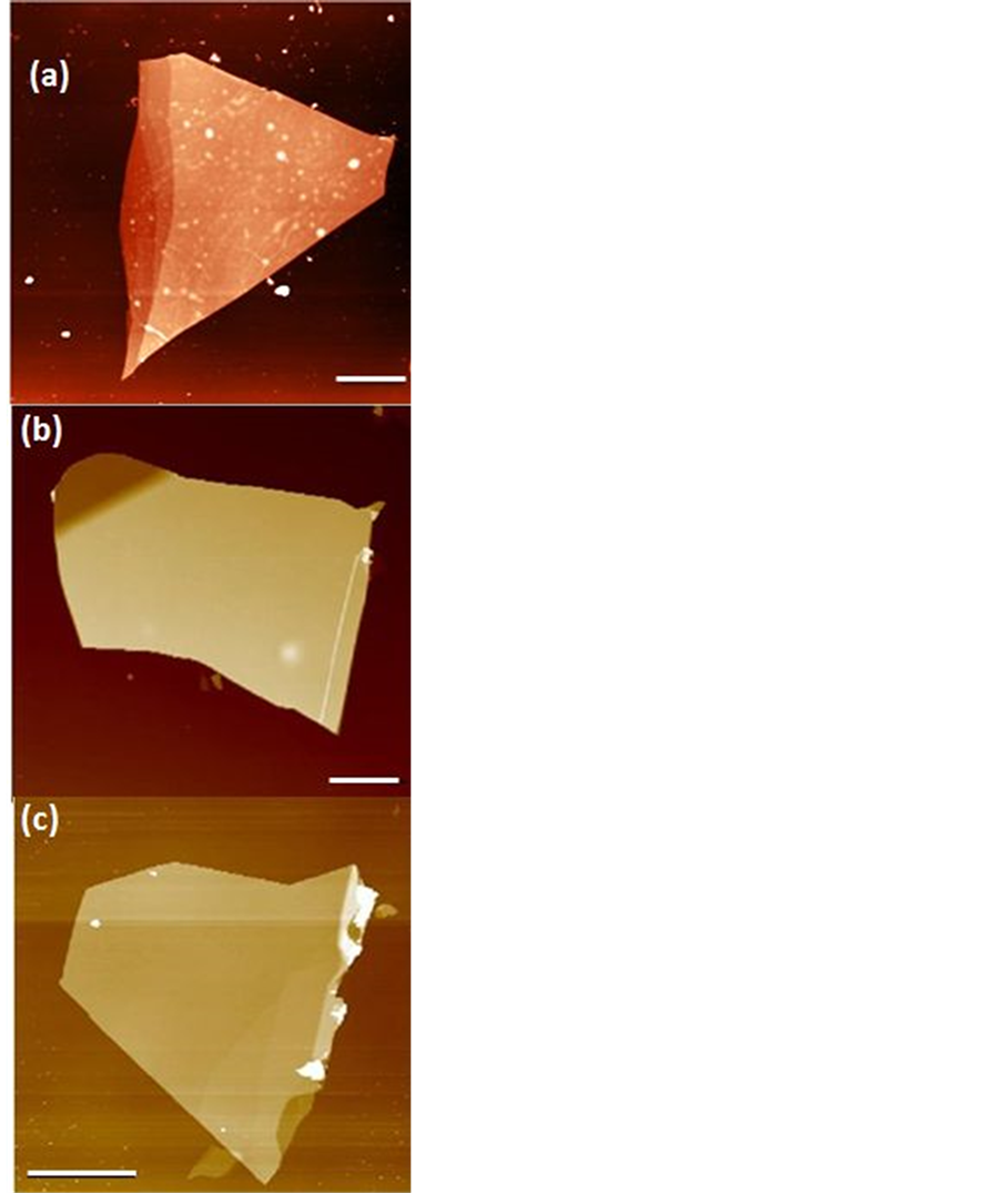
Figure 3. (Color online) AFM images show a comparison between a dirty (a) and a clean (b) hBN flake. (c) Image AFM of a hBN flake after thermal annealing in Ar/O2 atmosphere. Scale bar is 5 µm.
indicating that graphene flake in (a) has no more 4 layers and graphene sheet in (b) must have more than 3 layers. Moreover, FWHM (Full width half maximum) of 2D band increases as the layer thickness increases, which is associated with the electronic band structure near the K and K’ points. It is important to observe that the D mode (defect related mode) do not appear in these spectra, indicating the good quality of our exfoliated graphene sheets. It is also observed that the background signal due to PVA/PMMA film is absent in these spectra.
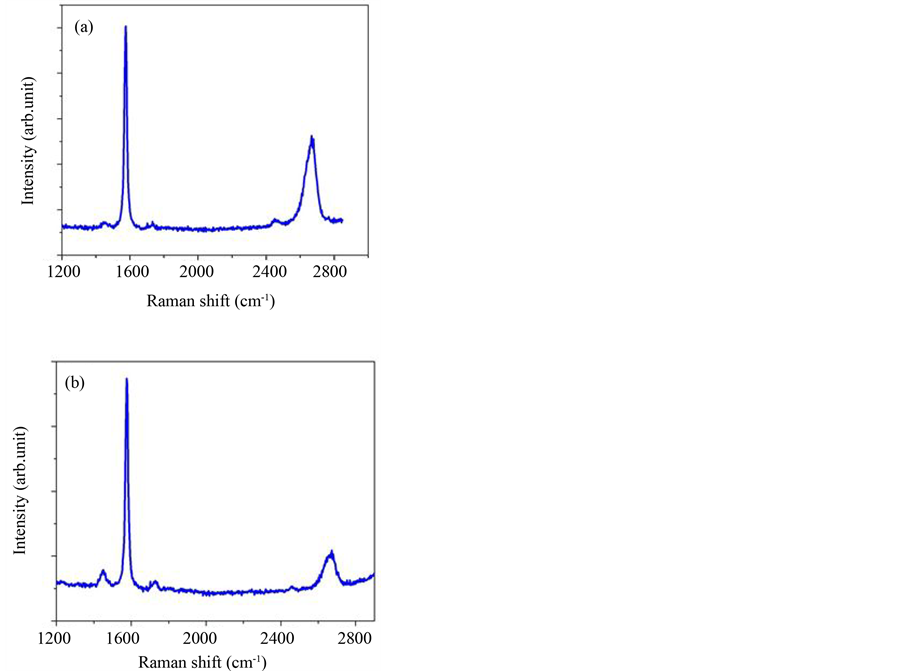
Figure 4. (Color online) Raman spectrum of two graphene flakes showing the G band peak and the 2D band peak. In (a) no more than 4 layers and (b) more than 4 layers.
Graphene that is transferred onto hBN before annealing show typical wrinkling as show in Figure 5(a) and Figure 5(b). Wrinkles and bubbles appear in somewhat different shapes and on the flat areas a rougher surface than usual is measured (0.9 nm rms roughness). This suggests that residues are likely to be present underneath. To prevent or minimize contamination from residues, we anneal at 400C in an Ar/H2 environment. The result is shown in Figure 5(c). The AFM image shows wrinkling on the hBN surface but, however the hBN had undergone a similar annealing treatment as shown in Figure 3(c). After transfer (at room temperature) the deposited graphene flake has many wrinkles and bubbles of up to 30 nm tall. After annealing some bubbles have disappeared and the size of the remaining bubbles increased or inflated. We observed that three clean surfaces of graphene and hBN still yield wrinkles and bubbles after transfer as indicated in Figure 5(c). However, the graphene sheet now has large flat areas where the graphene can be easily patterned in long Hall bars (1 µm wide and 10 µm long). Some bubbles coalescing into large bubbles were observed in graphene on SiOx. Samples with intentionally created bubbles [21] [22] have revealed that energy dispersive X-ray (EDX) and electron energy loss spectroscopy (LEEE) measurements in a cross section of a bubble mainly consist of hydrocarbons. The source of hydrocarbons is not clear. One explanation is that during transfer once the polymer scaffold is in close contact with target substrate polymer residues diffuse onto graphene due to mild heating of 110˚C. Another possibility could be a strong friction force between thermal expansion coefficients of graphene and hBN [23] , as claimed by Pan et al. [24] .
The Raman spectrum of this graphene flake taken after transfer is very similar to that taken before transfer (pristine) which provided evidence that the Ar/H2 process successfully removed all organic contaminants. These Raman spectra are composed of the known spectra of hBN and graphene (Figure 6(a)). A prominent and sharp peak arises around 1365 cm−1 in hBN spectra, which can be attributed to the Raman active LO-phonon in hBN [25] . It is important to distinguish this peak from the defect induced D-line appearing at around 1350 cm−1 [26] .
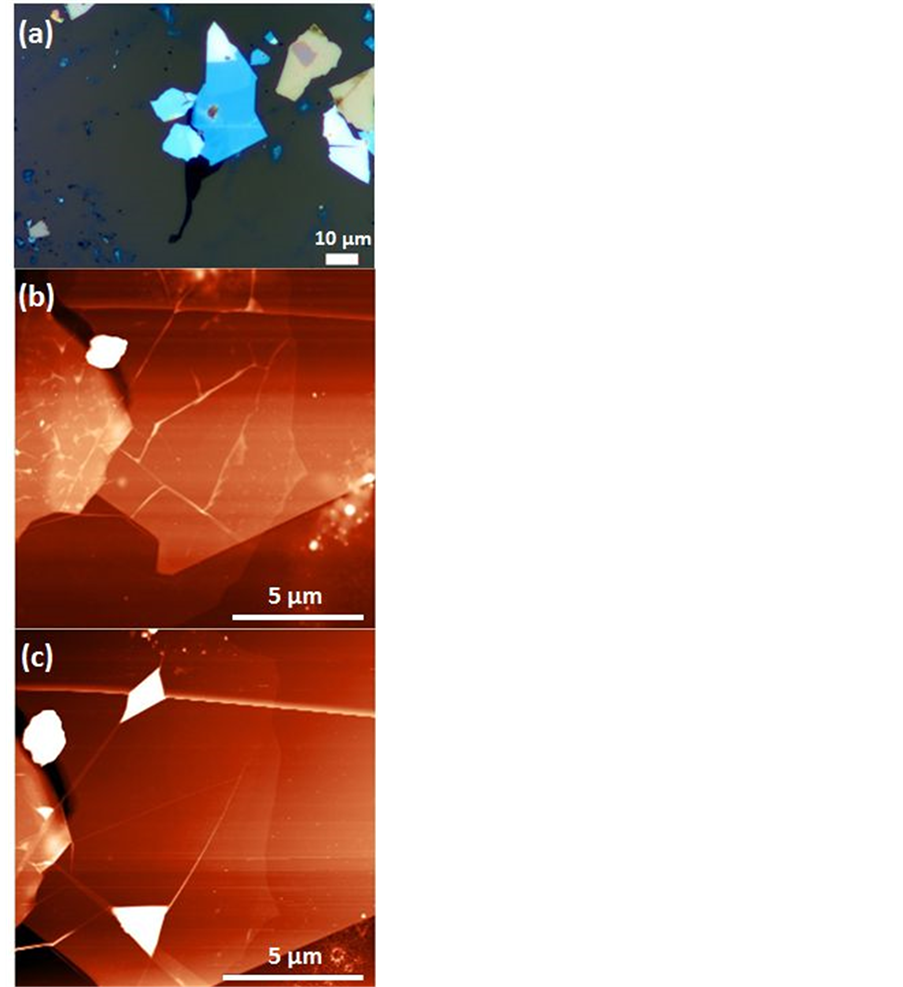
Figure 5. (Color online) (a) Optical image of dry transferred graphene before annealing; (b) An AFM image that shows wrinkles already present on the graphene surface; (c) After annealing treatment both wrinkles and bubbles have still appeared.
In order to show the substrate dependence of the Raman lines of graphene, we compare in Figure 6(a) and Figure 6(b) the lines of a flake that rest on hBN and another flake exfoliated on 300 nm SiO2. The G peak of graphene on hBN and the one on SiO2 differ significantly in their position. The G peak of graphene on SiO2 is centered at 1586.0 cm−1 while the one on hBN is centered at 1582.5 cm−1. The downshift can be attributed to reduced doping, which is also consistent with the decrease of the full width at half maximum (FWHM) of the G peak of graphene on hBN [27] . The FWHM is 14.2 cm−1 on SiO2 and 11.6 cm−1 on hBN. Also the 2D peak shows a substrate dependence of the position which is 2690 cm−1 on SiO2 and 2677 cm−1 on hBN, as illustrated in Figure 6(b). The graphene Raman spectra seems to be characteristic of three layer graphene, and there is no
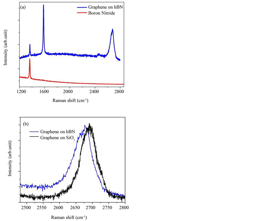
Figure 6. (Color online) (a) Measured Raman spectra of graphene trilayer transferred on hBN/SiO2 (blue color) and the spectrum of hBN/SiO2 alone (red color). This sample was heat treated in Ar/H2 at 400˚C after transferred. For comparison in (b) shows the 2D band Raman spectra of graphene trilayer on hBN and on SiO2 substrate.
detectable defect-related D band, suggesting that this thermal annealing not damage graphene, and raising the possibility that our cleaning procedure can be applied on hBN and graphene, and facility the preparation of devices involving multiple layers [28] .
3.2. Electrical Characterization of Graphene Devices
We found that anneal step in Ar/H2 flow degrades our contacts so we omitted this step here. Also no other annealing steps have been used; keeping the fabrication process the same as for SiO2-based devices. Typically the resistance between two contacts is in order of ~1.0 - 2.5 KΩ. Next we performed electrical transport measurements in order to estimate the charge mobility. We contacted Cr/Au electrodes to five wrinkled MLG flakes. A typical device is shown in the inset of Figure 7. Electrical measurements are performed using standard lock-in techniques with excitation current up to 1µA. We will show only results concerning the fabrication of the device with three layer graphene. In a four-point field effect transistor (FET) geometry we measure the resistance as a function of applied back gate, Figure 7. We extract the gate induced charge density in the graphene flake n = Cg/e(Vg – VD), where Vg is the applied gate voltage, VD is the gate voltage at which the charge neutrality point is found (VD = 10 V), and Cg = 100 µF∙m−2 is the geometric gate capacitance for 285 nm SiO2 and 20 nm hBN. The
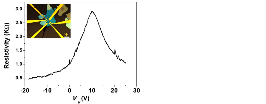
Figure 7. (Color online) Resistance as a function of the backgate voltage for graphene trilayer on h-BN after thermal annealing. Inset shows the graphene flake fabricated by e-beam lithography in a Hall bar geometry. Scale bar is 10 µm.
mobility is determined as µ = 1/neρ, where ρ is the resistivity of the flake. The field-effect mobility of this devices reaches 7200 cm2/V∙s at 4 K at high density of carries of 18.5 ´ 1011 cm−2. This mobility is about one order of magnitude higher than previously reported values for supported values [29] and [30] and the reduction in full width at half maximum of the Dirac peak indicates smaller fluctuation in charge-carrier density for the hBN supported graphene flake. We find that despite omitting cleaning steps after fabrication of devices; the charge transport quality was improved compared with that of SiO2-based graphene devices.
4. Conclusion
A methodology for fabricating graphene electronic devices on commercially obtained hBN is presented. We show that commercially obtained hBN, which is available in large amounts, offers a good alternative to noncommercial ultrapure hBN. We described a mechanical transfer method to deposit graphene on hBN substrates in order to fabricate graphene devices employing a mechanical co-lamination and transfer process. Additionally, since the fabrication recipe we developed requires only one cleaning step, it allows for fast device preparation of graphene on hBN with a little bubbles and wrinkles. Electrical transport measurements of the graphene devices on hBN have mobilities and carrier inhomogeneity that are almost an order of magnitude better than devices on SiO2. We think that this work can contribute in performing of atomic engineering of graphene on hBN, and sheds light on fundamental research as well as electronic applications based graphene/hBN heter-structures in the route of continual investigations of single-layer, bilayer and few-layer graphene.
Acknowledgements
The authors would like to acknowledge to Professor R. Ando and Professor Y. Pusep for their valuable supports to this research. CNPq and FAPESP (Brazilian agencies) for financial support.
References
- Novosolev, K.S., Geim, A.K., Morosov, S.V., Jiang, D., Zhang, Y., Dubonos, S.V., Grigorieva, I.V. and Firsov, A. (2004) Electrical Field Effect in Atomically Thin Carbon Films. Science, 306, 666-669. http://dx.doi.org/10.1126/science.1102896
- Ando, T. (2006) Screening Effect and Impurity Scattering in Monolayer Graphene. Journal of Physics Society of Japan, 75, Article ID: 074716. http://dx.doi.org/10.1143/JPSJ.75.074716
- Ishigami, M., Chen, J.H., Cullen, W.G., Fuhrer, M.S. and Williams, E.D. (2007) Atomic Structure of Graphene on SiO2. Nano Letters, 7, 1643-1648. http://dx.doi.org/10.1021/nl070613a
- Chen, J.H., Jang, C., Xiao, S., Ishigami, M. and Fuhrer, M.S. (2008) Intrinsic and Extrinsic Performance of Graphene Devices on SiO2. Nature Nanotechnology, 3, 206-209. http://dx.doi.org/10.1038/nnano.2008.58
- Deshpande, A., Bao, W., Miao, M., Lau, C.N. and LeRoy, B.J. (2009) Spatially Resolved Spectroscopy of Monolayer Graphene on SiO2. Physics Review B, 79, Article ID: 205411. http://dx.doi.org/10.1103/PhysRevB.79.205411
- Bolotin, K.I., Sikes, K.J., Jiang, Z., Klima, M., Fudenberg, G., Hone, J., Kim, P. and Stomer, H.L. (2008) Ultrahigh Electron Mobility in Suspended Graphene. Solid State Communications, 146, 351-355. http://dx.doi.org/10.1016/j.ssc.2008.02.024
- Trombos, N., Veligura, A., Junesch, J. and Berg, J.J.V.D. (2011) Large Yield Production of High Mobility Freely Suspended Graphene Electronic Devices on a Polydimethylglutaramide Based Organic Polymer. Journal of Applied Physics, 109, Article ID: 093702. http://dx.doi.org/10.1063/1.3579997
- Bao, W., Miao, F., Chen, Z., Zheng, H., Jang, W., Dames, C. and Lau, C.N. (2009) Controlled Ripple Texturing of Suspended Graphene and Ultrathin Graphite Membranes. Nature Nanotechnology, 4, 562-566. http://dx.doi.org/10.1038/nnano.2009.191
- Zhang, Y., Tan, Y.-W., Stomer, H.L. and Kim, P. (2005) Experimental Observation of the Quantum Hall Effect and Berry’s in Graphene. Nature, 438, 201-204. http://dx.doi.org/10.1038/nature04235
- Novoselov, K.S., McCann, E., Morosov, S.V., Fal’ko, V.I., Katsnelson, M.I., Zeitler, U., Jian, D., Schedin, F. and Geim, A.K. (2006) Unconventional Quantum Hall Effect and Berry’s Phase of 2π in Bilayer Graphene. Nature Physics, 2, 177-180. http://dx.doi.org/10.1038/nphys245
- Dean, C.R., Young, A.F., Meric, I., Lee, C., Wang, L., Sorgenfrei, S., Watanabe, K., Taniguchi, T., Kim, P., Shepard, K.L. and Hones, J. (2010) Boron Nitride Substrates for High-quality Graphene Electronics. Nature Nanotechnology, 5, 722-726. http://dx.doi.org/10.1038/nnano.2010.172
- Zomer, P., Dash, S.P., Tombros, N. and van Wees, B.J. (2011) A Transfer Technique for High Mobility Graphene on Commercially Available Hexagonal Boron Nitride. Applied Physics Letters, 99, Article ID: 232104. http://dx.doi.org/10.1063/1.3665405
- Xue, J., Sanchez-Yamagishi, J., Bulmash, D., Jacquod, P., Deshpande, A., Watanabe, K., Tanigushi, T., Jarillo-Herrero, P. and LeRoy, B.J. (2011) Scanning Tunnelling Microscopy and Spectroscopy Ultra-Flat Graphene on Hexagonal Boron Nitride. Nature Materials, 10, 282-285.
- Dean, C.R., Young, A.F., Cadden-Zimansky, P., Wang, L., Ren, H., Watanabe, K., Tanigushi, T., Kim, P., Hone, J. and Shepard, K.L. (2011) Multicomponent Fractional Quantum Hall Effect in Graphene. Nature Physics, 7, 1-4. http://dx.doi.org/10.1038/nphys2007
- Amet, F., Williams, J.R., Watanabe, K., Taniguchi, T. and Goldhaber-Gordon, D. (2011) Insulator Behavior at the Charge Neutrality Point in Single-Layer Graphene. Physics Review Letters, 110, Article ID: 216601. http://dx.doi.org/10.1103/PhysRevLett.110.216601
- Taychatanapat, T., Watanabe, K., Taniguchi, T. and Jarillo-Herrero, P. (2011) Quantum Hall Effect and Landau-Level Crossing of Dirac Fermions in Trilayer Graphene. Nature Physics, 7, 621-625. http://dx.doi.org/10.1038/nphys2008
- Mayorov, A.S., Gorbachev, R.V., Morozov, S.V., Britnell, L., Jalil, R., Ponomarenko, L.A., Blake, P., Novoselov, K.S. Watanabe, K., Tanigushi, T. and Geim, A.K. (2011) Micrometer-Scale Ballistic Transport in Encapsulated Graphene at Room Temperature. Nano Letters, 11, 2396-2399. http://dx.doi.org/10.1021/nl200758b
- Garcia, A.G.F., Neumann, M., Amet, F., Williams, J.R., Watanabe, K., Taniguchi, T. and Goldhaber-Gordon, D. (2012) Effective Cleaning of hexagonal Boron Nitride for Graphene Devices. Nano Letters, 12, 4449-4454. http://dx.doi.org/10.1021/nl3011726
- Blake, P., Hill, E.W., Castro Neto, A.H., Novoselov, K.S., Jiang, D., Yang, R., Booth, T.J. and Geim, A.K. (2007) Making Graphene Visible. Applied Physics Letters, 91, Article ID: 063124. http://dx.doi.org/10.1063/1.2768624
- Jungen, A., Popov, V.N., Stampfer, C., Durrer, L., Stoll, S. and Hierold, C. (2007) Raman Intensity Mapping of Singled-Walled Carbon Nanotubes. Physics Review B, 75, Article ID: 041405(R). http://dx.doi.org/10.1103/PhysRevB.75.041405
- Stolyarova, E., Stolyarov, D., Bolotin, K., Ryu, S., Liu, L., Rim, K.T., Klima, M., Hybertsen, M., Pogorelsky, I., Pavlishin, I. Kusche, K. Hone, J., Kim, P., Stomer, H.L., Yakimenko, V. and Flynn, G. (2009) Observation of Graphene Bubbles and Effective Mass Transport under Graphene Films. Nano Letters, 9, 332-337. http://dx.doi.org/10.1021/nl803087x
- Haigh, S.J., Gholinia, A., Jalil, R., Romani, S., Britnell, S., Elias, D.C., Novoselov, K.S., Ponomarenko, L.A., Geim, A.K. and Gorbachev, R.V. (2012) Cross-Sectional Imaging of Individual Layer and Buried Interfaces of GrapheneBased Heterostructures and Superlattices. Nature Materials, 11, 764-767. http://dx.doi.org/10.1038/nmat3386
- Geim, A.K. and Novoselov, K.S. (2007) The Rise of Graphene. Nature Materials, 6, 183-191. http://dx.doi.org/10.1038/nmat1849
- Pan, W., Xiao, J., Zhu, J., Yu, C., Zhang, G., Ni, Z., Watanabe, K., Taniguchi, T., Shi, Y. and Wang, X. (2012) Biaxial Compressive Strain in Graphene/Boron Nitride Heterostructures. Scientific Reports, 2, Article Number: 893. http://dx.doi.org/10.1038/srep00893
- Geick, R., Perry, C. and Rupprecht, G. (2006) Normal Modes in Hexagonal Boron Nitride. Physics Review, 146, 543. http://dx.doi.org/10.1103/PhysRev.146.543
- Graf, D., Molitor, F., Ensslin, K., Stampfer, C., Jungen, A., Hierold, C. and Wirtz, L. (2007) Spatially Resolved Raman Spectroscopy of Singleand Few-Layer Graphene. Nano Letters, 7, 238-242. http://dx.doi.org/10.1021/nl061702a
- Yan, J., Zhan, Y., Kim, P. and Pinczuk, A. (2007) Electrical Field Effect Tuning of Electron-Phonon Coupling in Graphene. Physics Review Letters, 98, Article ID: 166802. http://dx.doi.org/10.1103/PhysRevLett.98.166802
- Britnell, L., Gorbachev, R.V., Jalil, R., Belle, B.D., Shedin, F., Mishchenko, A., Georgiou, T., Katsnelson, M.I., Eaves, L., Morosov, S.V., Peres, N.M.R., Leist, J., Geim, A.K., Novoselov, K.S. and Ponomarenko, L.A. (2012) Field-Effect Tunneling Transistor Based on Vertical Graphene Heterostructures. Science, 335, 947-950. http://dx.doi.org/10.1126/science.1218461
- Kumar, A., Escoffier, W., Poumirol, J.M., Fangeras, C., Arovas, D.P., Fogler, M.M., Guinea, F., Roche, S., Goiran, M. and Raquet, B. (2011) Integer Quantum Hall Effect in Trilayer Graphene. Physics Review Letters, 107, Article ID: 126806. http://dx.doi.org/10.1103/PhysRevLett.107.126806
- Zhu, W., Perebeinos, V., Freitag, M. and Avouris, P. (2009) Carrier Scattering, Mobilities, and Electrostatic Potential in Monolayer, Bilayer, and Trilayer Graphene. Physics Review B, 80, Article ID: 235402. http://dx.doi.org/10.1103/PhysRevB.80.235402
NOTES

*Corresponding author.