Advances in Nanoparticles
Vol.3 No.1(2014), Article ID:42714,4 pages DOI:10.4236/anp.2014.31001
Synthesis of Ag/Ag2S Nanoclusters Resistive Switches for Memory Cells
National Research University of Electronic Technology, Zelenograd, Russia
Email: msomeone@gmail.com
Copyright © 2014 Aleksey Nikolaevich Belov et al. This is an open access article distributed under the Creative Commons Attribution License, which permits unrestricted use, distribution, and reproduction in any medium, provided the original work is properly cited. In accordance of the Creative Commons Attribution License all Copyrights © 2014 are reserved for SCIRP and the owner of the intellectual property Aleksey Nikolaevich Belov et al. All Copyright © 2014 are guarded by law and by SCIRP as a guardian.
Received November 28, 2013; revised December 21, 2013; accepted January 9, 2014
KEYWORDS
Silver Sulphide Clusters; Memory Cells; Sulphidation; Deal-Grove Model
ABSTRACT
Resistive switching Ag/Ag2S nanoclusters were formed by sulphidation of melting-dispersed thin and continuous Ag films. The morphology, structure and electrical properties of the prepared clusters were characterized by scanning (SEM), transmitting electron (TEM), scanning resistance microscopes (SRM) and Raman scattering. Hysteretic resistive switching behavior was observed in the samples that were studied with ON/OFF switching voltage equal to 8 - 10 V respectively. Simple empirical numerical simulation model, based on Deal-Grove model assumptions and mechanisms, for silver nanoclusters sulphidation process, was proposed.
1. Introduction
Nonvolatile memory unit is an important component of microelectronic/nanoelectronic devices and has aroused scientific and commercial interest [1-5]. A lot of ongoing researches concern a very promising field: resistive switches based on structures containing solid-state electrolyte encased between two metal electrodes.
Switching time in those structures depends on the choice of transition layer type greatly, where primarily the choice between insulating or solid electrolyte materials has to be made.
The state of the art in resistive memory switching latency that was currently reached comes out just too few nanoseconds compared to other memory types where it is larger by two magnitudes. The storage duration for resistive switches can reach up to ten years in 70˚C - 130˚C range [6].
Electronic components still tend to decrease in size during this decade, including resistive memory devices. It provides a way to produce resistive switches with nanometer scale. Application of self-organization phenomena to resistive switch arrays’ production has been widely studied during the last years as a promising alternative to classic methods. Thus, authors suggested that silver/silver sulphide nanowhiskers formed in porouse alumina membrane as a material for resistive switches’ arrays [3,5,7]. But high mechanical and thermal instabilities of the structure mentioned above make its use impractical for full production cycle of resistive memory devices. This problem is addressed in [6] using arrays of Ag/Ag2S nanoclusters synthesized with vacuum deposition on wafer through porous alumina membrane used as a mask. But this method is hardly reproducible due to membrane fragility and the isotropy of the sputtering process.
A simple and reproducible silver thin film meltingdispersion for initial silver nanoclusters formation was suggested in this paper. Full-scale study of silver nanocluster arrays’ sulphidation process was presented. Composition and electrical measurements of obtained Ag/ Ag2S samples were taken. The statistical properties of obtained samples that were derived were used to introduce simple numerical simulation model of sulphidation process.
2. Experiment
All samples were prepared on pre-cleaned polished surface of monocrystal boron doped 75 mm silicon wafers (Si (100), ρ = 0.85 - 1.15 Ohm·cm). Wafer’s pre-cleaning process was done as follows: washing in Caro's acid solution (H2SO4:H2O2 = 1:4), cleaning in deionized water (ρ = 17 Ohm·cm) and drying in isopropyl alcohol vapors. Amorphous carbon and copper films were deposited with magnetron sputtering (using sputter deposition equipment AXXIS Kurt Lesker) on working wafer surface of 10 nm and 1 um respectively. Vacuum thermal evaporation was used to obtain 10 nm silver thin films using SI 500 PPD, SENTECH.
Silver nanocluster arrays were formed by thermal annealing of 10 nm thick silver films at a temperature of 230˚C during 40 minutes in SI 500 PPD, SENTECH right after vacuum thermal evaporation. Melting-dispersion theory predicts that thin films split to separate clusters during annealing, which was observed during experiments on silver film annealing. Low-temperature sulphidation in hydrogen sulphide atmosphere in airtight chamber was used to obtain Ag2S particles. In this work, chemical reaction of 5 ml strong chlorohydric acid solution with 0.01 M sodium sulphide solution was used as a source of hydrogen sulphide as suggested in [8]. Sulphidation process time varied from 5 minutes to 16 hours. Obtained samples were annealed again at a temperature of 150˚C to remove free sulphur and water in SI 500 PPD, SENTECH.
Electrical properties of prepared samples were studied using Solver P-47 SRM (NT-MDT). Fabricated solid state Ag2S electrolyte formulation was studied using Raman scattering on Cantaur I HR complex (Nanoscantech). Same method was used for studying Ag2S powder spectrum used as a reference. Ag2S powder was synthesized by slowly mixing 0.1 M Na2S and 0.01 M AgNO3 solutions until getting solid black solution which was then filtered through blotting paper. Sample surfaces were studied using SEM and TEM.
3. Results and Discussion
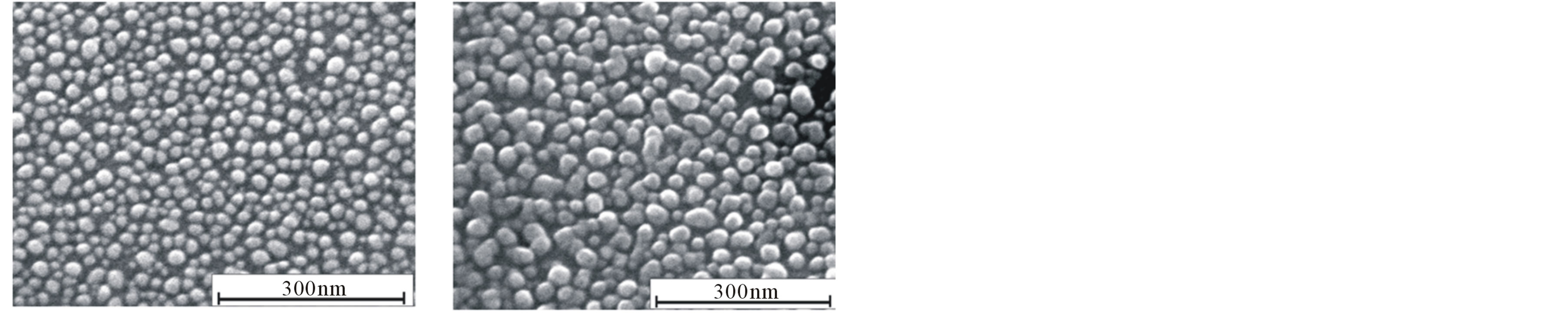
Ag and Ag/Ag2S SEM images are shown in Figures 1(a) and (b) respectively. Ag/Ag2S clusters and Ag2S powder Raman spectras are presented in Figure 1(c). Comparison of spectras in Figure 1(c) confirms that silver sulphide appears on sample’s surface. TEM image (Figure 2) analysis reveals that silver sulphide formation occurs on silver clusters surface.
Figure 3 shows Ag/Ag2S nanoclusters array I-V characteristics, measured by SRM, which correspond to typical I-V characteristic of Resistive Switching materials. Thus, obtained silver sulphide nanoclusters could be considered as resistive switching material. Array of the Ag/Ag2S structure exhibits repeated ON/OFF states under voltage sweeps.
Thus, obtained silver sulphide clusters could poten tially be used as resistive switching material. Ag2S for-
 (a)
(a)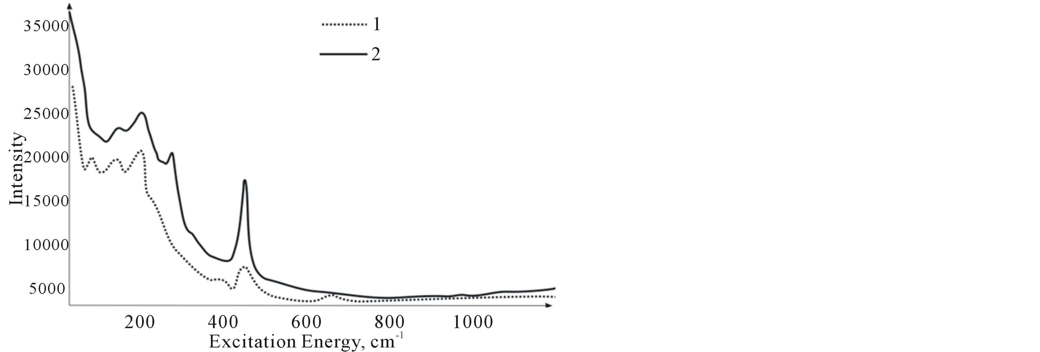 (b)
(b)
Figure 1. Silver nanoclusters formed on Cu/C surface of silicon wafer SEM image (а), silver sulphide nanoclusters after 16 hours SEM image (b), Raman spectra of Ag/Ag2S nanoclusters (1) compared to powder (2) spectra.
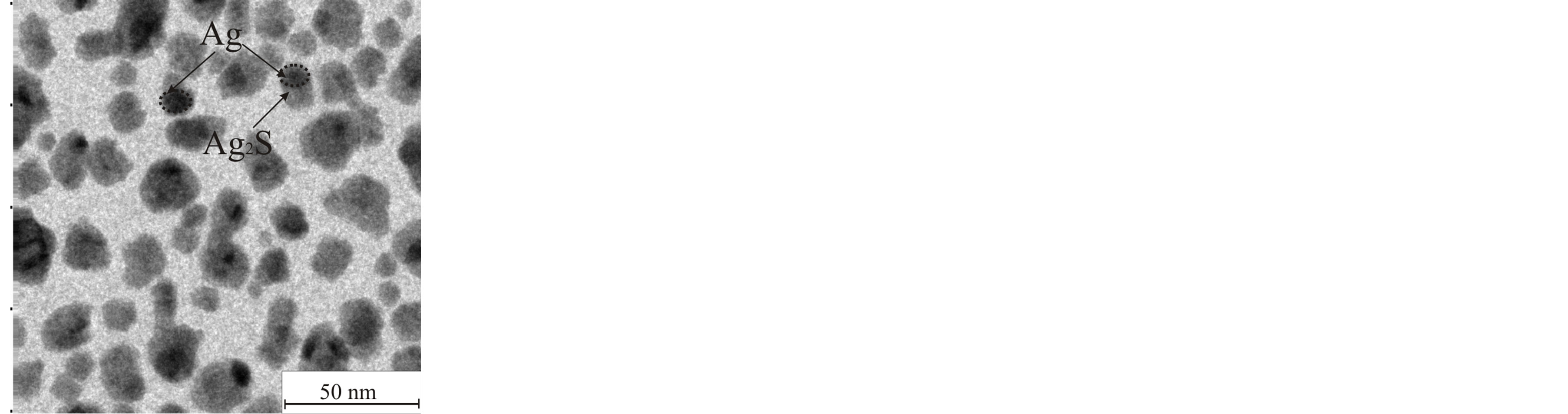
Figure 2. TEM image of sulphidized silver nanoclusters array.
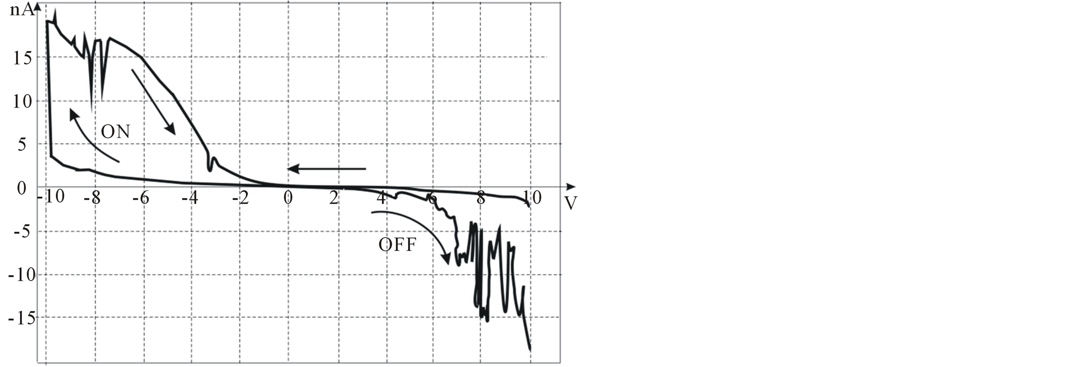
Figure 3. Volt-amps for Ag2S synthesized on samples, measured by SRM.
mation during sulphidation process may be described with a chemical reaction:
 (1)
(1)
According to Equation (1) it is possible to calculate volume ratio between silver sulphide and silver. It was established that this ratio is 1.65. During experiments a total of 60 wafer samples were obtained (10 samples for each of 6 exposure durations), all with different sulphidation times, which were later used to gather statistical distributions for cluster diameters. Cluster diameters and their distributions were measured by AXIO Vision software using AutoMeasure Plus module (which provides histograms for any image-based quantities). Those distributions were close to Gaussian. Averages of each 10 means corresponding to the same H2S exposure times (5, 100, 195, 240, 370, 480, 620 and 900 minutes) were used to study how cluster diameter depends on time presented in Figure 4. It was observed that sulphide thickness is directly proportional to sulphidation time and could be described using linear-parabolic law. This behavior is similar to the one observed during silicon oxidation in dry or wet oxygen atmosphere which could be described using Deal-Grove model [9].
Cluster diameter dependence plot was used to calculate linear and parabolic constants for Deal-Grove model. These constants were used for numerical simulations that will be described later on.
We introduce empirical simulation model describing silver nanoclusters arrays’ sulphidation process which has been used in the later experiments to predict parameters of forming structures: clusters’ diameters and silver sulphide’s thickness. It is assumed that sulphidation reaction occurs at the sulphide–metal interface rather than at gas-sulphide interface because the probability of silver atoms’ diffusion to gas-sulphide interface at room temperature is about zero. When sulphidation process starts, it is assumed that silver clusters’ surfaces are free from silver sulphide, silver oxide, or their concentration could be neglected, and adsorbed water which evaporates during melt-dispersion. Thus, on the initial stage sulphidation process could be described as following:
• hydrogen sulphide and oxygen from reactor’s atmosphere adsorption appears on silver clusters’ surface;
• sulphidation reaction with silver atoms on free silver cluster surface appears.
It should be noted that during initial stage reactants adsorb at sulphidized parts of clusters’ surface, and sulphidation occurs in the same way as the one described below for later stages of sulphidation. Initial stage of sulphidation finishes when silver cluster surface is fully covered by silver sulphide layer. After that sulphidation process goes as following:
• hydrogen sulphide and oxygen from reactor’s atmos-
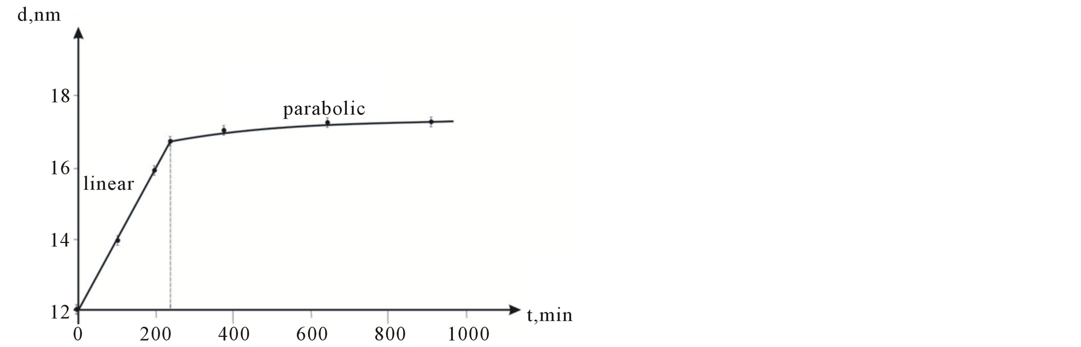
Figure 4. The dependence of sulphide clusters diameter on sulphidation time.
phere adsorption appear on silver sulphide clusters’ surface;
• reactants diffuse to sulphide-metal interface through sulphide layer;
• finally, sulphidation reaction with silver appears on silver sulphide-silver interface.
It is also assumed that described processes occur in steady state conditions. Usually, hydrogen sulphide gas is produced in significant quantity compared to the quantity of silver on reactive substrate. Thus, it can be assumed that ambient gases do not limit sulphidation reaction rate.
Numerical simulation of described empirical model was done on coupled lattice grid using Monte Carlo method. Custom software was developed using NVIDIA CUDA SDK running on Quadro K5000 GPU grid. Each cell of simulated coupled lattice grid has assigned quantities of each modeled chemical compound in described system: hydrogen sulphide, oxygen, silver and silver sulphide, wafer substance (all kinds of dopants are neglected). Wafer surface assumed as locally flat in simulated region, and initial silver clusters are modeled as ellipses with uniformly random angles of rotation and normal distribution of axes’ radiuses. Distributions choice seems to be a valid assumption according to clusters’ geometry statistics that was gathered by analyzing 60 samples with silver clusters after the melting-dispersion process. Assuming excessive amount of oxygen and hydrogen suplhide diffusion processes in gaseous phase could be not considered, and concentrations in reactor could be considered constant during all the modeled time interval for both gases. Hydrogen sulphide and oxygen diffusion through silver sulphide are modeled with simple diffusion equations, with diffusivity coefficients calculated from linear and parabolic constants. Silver sulphidation on metal-sulphide interface in simulation appears with probability that is proportional to chemical reaction rate, and leads to volume expansion of clusters which is evident on SEM image of Figure 1. This volume expansion could be explained with the difference in lattice parameter for silver sulphide and silver. This effect is also taken into consideration in the numerical simulation model that was described earlier, which helps to make more precise predictions against resulting sulphidized clusters’ geometrical parameters at certain experiment time.
Numerical simulation results were then visualized as volume renderings (using ray marching in OpenGL shader) and are shown in Figure 5.
As seen in Figure 4, mean cluster diameter that is obtained by numerical simulation is 12 nm at 0 minutes of sulphidation (the beginning of the process), 14 nm at 100 minutes (the middle of the linear stage) and 16 nm at 240 minutes (the beginning of the parabolic process stage). These results correlate with averaged experimental data shown in Figure 4.
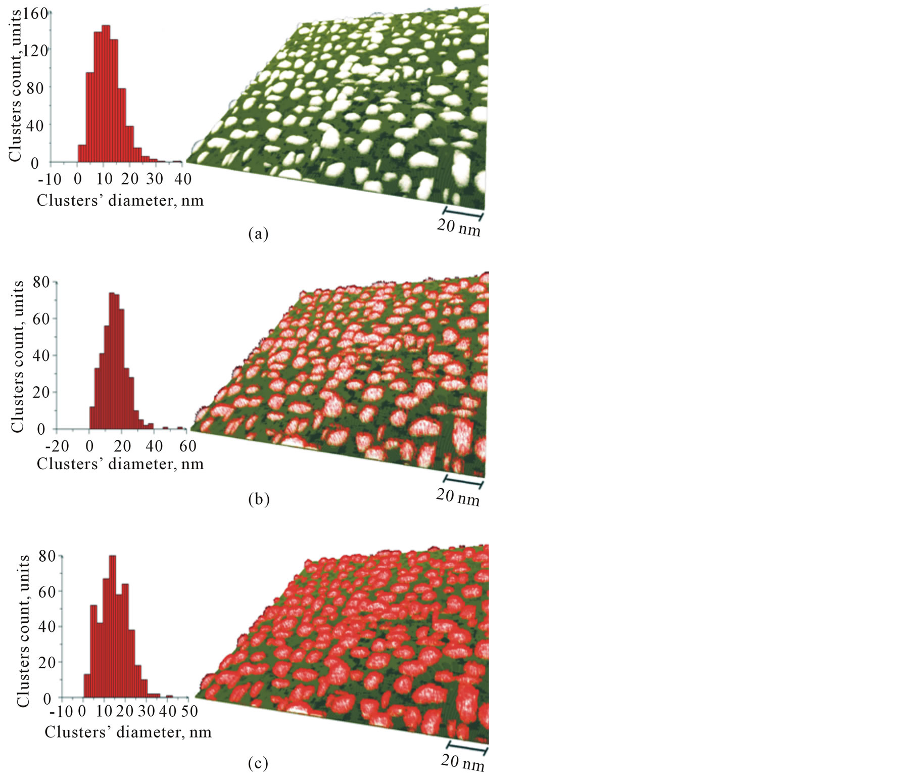
Figure 5. Silver nanoclusters sulphidation process simulation results that were obtained with volume rendering of coupled lattice grid (200 × 200 × 50 nm with 0.25 nm cell size) states at 0 (a), 100 (b) and 240 (c) minutes’ simulation time (colors legend: green—wafer, white—silver, red—silver sulphide).
4. Conclusions
In this study, the method for silver nanoclusters formation is proposed. It uses self-organization effects occurring in melting-dispersion process for silver thin film. This method allows increasing reproducibility and simplicity of the process, as opposed to sputtering through mask methods. The electrical properties and composition of the samples that were obtained by using the described process were studied. These studies reveal resistiveswitching behaviour of silver sulphide clusters that were obtained. Numerical simulation model of sulphide clusters growth based on Deal-Grove model and previous formation processes’ statistics was introduced to improve reproducibility and predict geometrical parameters of clusters’ formation processes that were carried out later.
Further intense research should be carried out to prove the stability of the obtained structure. The sulphide formation process should be studied in detail to specify the simulation model. The variety of samples’ characteristics at different process temperatures also generates interest.
REFERENCES
- M. Valentinova, “Memory and Electronic Semiconductor Elements,” Science, Technology, Business, Vol. 5, No. 10, 2003, pp. 10-15.
- R. Waser and M. Aono, “Resistively Switching Pt/Spin- On Glass/Ag Nanocells for Non-Volatile Memories Fabricated with UV Nanoimprint Lithography,” Nature Materials, Vol. 6, 2007, pp. 833-839.
- S. Thakoor, A. Moopenn, T. Daud and A. Thakoor, “Solid-State Thin-Film Memistor for Electronic Neural Networks,” Applied Physics, Vol. 67, No. 6, 1990, pp. 3132- 3135.
- N. Lee, B. An, A. Koo, H. Ji, J. Cho, Y. Choi, Y. Kim and C. Kang, “Resistive Switching Behavior in a Ni-Ag2Se-Ni Nanowire,” Applied Physics A, Vol. 102, No. 4, 2011, pp. 897-900. http://dx.doi.org/10.1007/s00339-011-6319-y
- S. Jou, B. Hwang and C. Li, “Resistance Switching Properties in Cu/Cu-SiO2/TaN Device,” Proceedings of the World Congress on Engineering, Vol. 1, 2011, pp. 1496- 1499.
- C. Hsiung, H. Liao, J. Gan, T. Wu, J. Hwang, F. Chen and M. Tsai, “Formation and Instability of Silver Nanofilament in Ag-Based Programmable Metallization Cells,” ACS Nano, Vol. 4, No. 9, 2010, pp. 5414-5420. http://dx.doi.org/10.1021/nn1010667
- B. Widrow, “RL Technical Report No. 1553-2 Electronics Research Laboratory,” Stanford University, 1960.
- D. Wang, L. Liu, Y. Kim, Z. Huang, D. Pantel, D. Hesse and M. Alexe, “Fabrication and Characterization of Extended Arrays of Ag2S/Ag Nanodot Resistive Switches,” Applied Physics Letters, Vol. 98, 2011, Article ID: 243109.
- C. Jaeger, “Richard Introduction to Microelectronic Fabrication,” Pearson Education, Inc., Upper Saddle River, 2002.