Advances in Nanoparticles
Vol. 1 No. 2 (2012) , Article ID: 21730 , 6 pages DOI:10.4236/anp.2012.12002
Nanoparticle Electromagnetic Properties for Sensing Applications
Department of Applied Electronics, Roma Tre University, Rome, Italy
Email: luigi.laspada@uniroma3.it, riovine@uniroma3.it, vegni@uniroma3.it
Received June 2, 2012; revised July 12, 2012; accepted August 5, 2012
Keywords: Nanoparticles; Analytical Models; Localized Surface Plasmon Resonance; Biomedical Applications
ABSTRACT
Nanoparticles play a crucial role in biomedical and sensing applications. In this paper the design of non-spherical gold nanoparticles, operating in the near infrared and visible regime, is proposed. The structures consist of metallic resonating inclusions of different shapes embedded in a dielectric environment. Different geometries, such as cube, elliptical cylinder and rod are considered. The main purpose of this study is to develop new analytical formulas useful in the nanoparticle design for specific biomedical and sensing applications. These analytical models are developed in order to describe the electromagnetic behavior of the nanoparticles in terms of resonant wavelength position, magnitude and amplitude width for absorption and scattering cross section. The obtained results are compared to the numerical ones, performed by full-wave simulations, and to the experimental values existing in literature. A good agreement among analytical, experimental and numerical results was obtained. Then, the structure is analyzed in terms of sensitivity properties. Exploiting the proposed analytical models, it is possible to design the nanostructures with the desired electromagnetic properties. The results show that these structures can be successfully applied for sensing applications.
1. Introduction
In the last few years there has been a huge interest in nanostructure fabrication, due to a wide variety of potential applications offered by their use. Nanoparticles are of great scientific interest as they possess particular properties, related to their size, shape, inclusion electromagnetic properties and to the refractive index of the surrounding dielectric environment [1].
When the nanoparticle is exposed to an electromagnetic source, the electromagnetic field response is highly localized near the nanostructure. In particular, the excitation of a Localized Surface Plasmon Resonance (LSPR), at the nanoparticle resonant frequency, results in a strong local enhancement of the electromagnetic field at the nanostructure surface. The interaction between the electromagnetic field and the surrounding dielectric environment is restricted to a small area, reaching a very high sensitivity.
Such phenomenon is the principle underlying several sensing applications and different lab-on-a-chip sensors. In fact, the optical properties derived from LSPR make gold nanoparticles suitable for several application areas, such as optics and photonics [2,3], biochemical sensing and detection [4,5], protein analysis [6,7], cell membrane function [8], biomedical applications [9,10], electron microscopy [11], electronics [12], nanotechnology [13] and materials science [14].
The main advantages in using nanoparticles as sensors are:
• A reduction in the structure size, without affecting sensitivity. Light intensity enhancement is a very important aspect in LSPR sensors, while the electromagnetic localization means that such structures have a very high spatial resolution, limited only by the size of nanoparticles. As a consequence, the sample volume required for sensing applications is reduced by several orders of magnitude.
• The possibility of arranging nanoparticles in an array configuration and tuning their resonance to coincide with spectral characteristics of a selected in/organic chemical group. This can turn out to be useful for molecules detection.
• Increasing bio-sensing system performances: due to the small structure size, different arrays of resonators can be implemented on a single sensing platform to detect different biological samples simultaneously.
Thus, it stands to reason that such structures are expected to become crucial for a wide range of applications: although many academic researches have realized and experimentally demonstrated their capability, little is known about the nanostructure analytical models, useful to describe their resonant behavior. To solve the electromagnetic problem for any inclusion geometry it is necessary to understand their electromagnetic behavior and develop design formulas useful for their implementation. The possibility of predicting, by proper analytical models, the electromagnetic behavior of different kinds of structures is of considerable interest in order to build up inclusions that satisfy certain requirements.
Starting from this background, this research attempts to present a design method for a selected group of nanoparticles with desired electromagnetic properties.
Thus, the paper mean objectives are:
• Developing new analytical models for the nanoparticles considered, in order to describe their resonant behavior;
• Studying the structures in terms of sensitivity, in order to verify their capability to be used as a sensing platform;
• Comparing the electromagnetic properties in order to choose the structure that best suits to specific applications.
The main advantage is the possibility to tune the nanoparticle resonance by changing its geometrical and electromagnetic properties.
The nanostructure proposed in this study consists of metallic resonating inclusions of different shape embedded in a dielectric environment. An electromagnetic source excites the nanostructure under study and the nanoparticle electromagnetic properties are revealed in terms of absorption and scattering cross section. In particular, the nanostructure has a specific resonant frequency in terms of position, magnitude and amplitude width, depending on its geometrical (shape, dimensions) and electromagnetic characteristics.
In this paper a comprehensive study of the electromagnetic properties of the following geometrical cases is proposed: cube, nanorod and elliptical cylinder.
The article is structured as follows: firstly, new analytical models describing the electromagnetic behavior of the considered nanostructures are presented, in order to correlate their geometrical and electromagnetic parameters with their resonant frequency properties (wavelength position, magnitude and amplitude width) in terms of absorption and scattering cross sections.
Secondly, the results obtained by the proposed models are compared to the ones performed by full-wave simulations and to the experimental values existing in literature. Then, the sensitivity properties of the structure are analyzed in order to optimize it, according to the specific application required.
2. Analytical Models and Electromagnetic Properties of Non-Spherical Nanoparticles
In this Section, new analytical models describing the nanoparticle electromagnetic behavior are presented. The target is to develop new analytical closed form formulas for the design of such nanostructures.
Let’s assume that the structure is excited by an impinging plane wave, having the electric field parallel and the propagation vector k perpendicular to the nanoparticle principal axis, as depicted in Figure 1, where the single particle is shown.
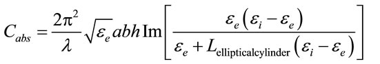
Specifically, the electromagnetic properties of gold cube, nanorod and elliptical cylinder in terms of absorption (Cabs) and scattering cross section (Csca), are quantified.
The geometrical parameters considered are shown in Figure 1. The cube length l, the elliptical cylinder semiaxes a and b, the rod thickness ar and the height of the whole structures h.
Let’s point out some relevant aspects concerning the carried out study:
• For gold nanoparticles, experimental values [15] of the complex permittivity function have been inserted;
• The surrounding dielectric medium is considered to be vacuum.
For gold nanostructure the electromagnetic absorption and scattering cross section are performed by using fullwave simulation code, through the integration commercial code CST Studio Suite [16]. In the following subsections a new electromagnetic study, for all the nanostructure considered, is proposed.
2.1. Nanoparticle Absorption and Scattering Cross-Section Design Formulas
In order to study the nanoparticle electromagnetic field distribution when an oscillating electromagnetic field interacts with a metallic nanoparticle, some assumptions must be done.
First of all, let’s assume that the particle size is much smaller than the wavelength in the surrounding medium [17]: under the limit of “electrically” small particles the electromagnetic field is approximately constant over the particle volume. Therefore the resonant behavior of the

Figure 1. Geometrical sketch of the nanostructures: (a) Cube; (b) Rod; (c) Elliptical cylinder. Geometrical parameters: l = cube side length; a,b = elliptical cylinder base semiaxes lengths; ar = rod thickness; h = height length of the whole structures.
individual structure can be studied in terms of a quasi-static approximation.
Secondly, the considered particle is homogeneous and isotropic and the surrounding material is a homogeneous, isotropic and non-absorbing medium: in such conditions we can relate the nanoparticle macroscopic dielectric function to its microscopic polarizability. Therefore, in order to develop an accurate analytical model it is crucial to find out the expression of the polarizability for the nanostructure considered. Typically the particle polarizability can be expressed as [18]:
 (1)
(1)
where V is the particle volume, εe is the electric permittivity of the surrounding dielectric environment, εi is the particle electric permittivity and L is the depolarization factor.
Following the same procedure [19], new depolarization factors for the selected particles have been developed. Starting from such factors, it is possible to develop new analytical closed-form formulas for the scattering and absorption cross-section of the aforementioned particles.
The general absorption (Cabs) and scattering (Csca) crosssection expressions read:
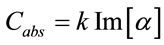 (2)
(2)
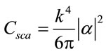 (3)
(3)
where  is the wave number, λ is the wave length and n is the refractive index of the surrounding dielectric environment. Considering such elements and the electric field polarization of the impinging plane wave, the absorption cross-section follows:
• Cube:
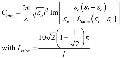 (4)
(4)
• Nanorod:
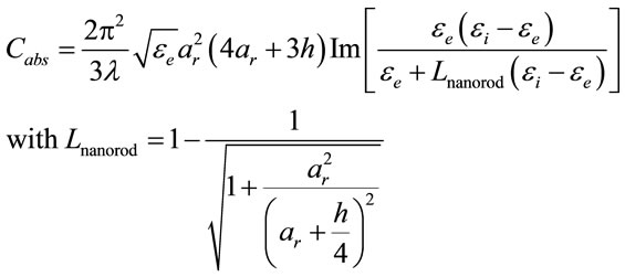 (5)
(5)
• Elliptical cylinder:
 (6)
(6)
where E is the Complete Elliptic Integral of the second kind, εe the surrounding medium electric permittivity, εi the inclusion permittivity, l the cube side length, a and b the elliptical cylinder base semi-axes lengths, ar the rod thickness, h the height length of the whole structures and .
.
It is worth noting that if the elliptical cylinder degenerates into a regular cylinder (a = b), the polarizability coincide with the classical formula existing in literature [19].
For the sake of brevity, only the absorption terms are shown here, but the same formulas can be obtained for the scattering one.
2.2. Comparison between Analytical Model, Numerical and Experimental Values
Using the analytical models reported in the previous section, it is possible to calculate analytically the inclusion resonant wavelengths. In this sub-section numerical results, performed by full-wave simulations, are compared to the theoretical ones, obtained from the proposed model, and to the experimental values [20-22], for different geometrical parameter configurations, as reported in Table 1. The surrounding dielectric medium is considered to be water with a complex refractive index n=1.33 + j0 at all wavelengths.
The relative analytical-numerical errors and analyticalexperimental ones have been calculated and reported in Table 1. Their expressions read, respectively:
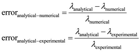 (7)
(7)
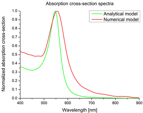
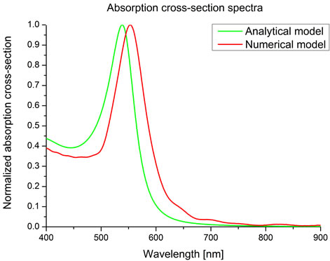
In Figure 2, an example of absorption cross-section spectra for the selected nanoparticles is presented.
3. Effect of Geometrical and Electromagnetic Parameters
From the obtained analytical models it is clear that a relation between the nanoparticle resonant frequency, its geometrical parameters (dimensions, particle volume), the
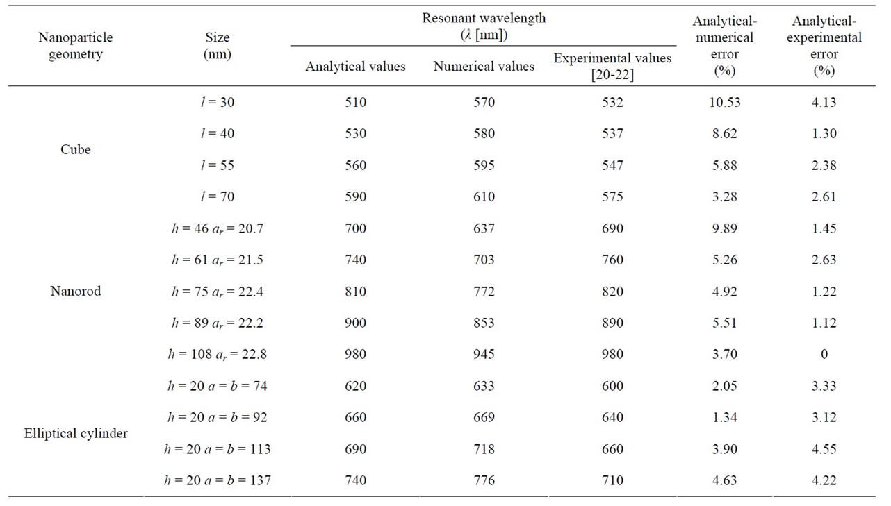
Table 1. Comparison of resonant wavelengths for the considered inclusions.
 (a) l = 80 nm
 (b) h = 40 nm, ar = 20 nm
 (c) h = 20 nm, a = 40 nm, b = 20 nm
Figure 2. Comparison among analytical and numerical models for: (a) Cube; (b) Nanorod; and (c) Elliptical cylinder.
metallic material electromagnetic properties (real permittivity εreal, losses εimm), and the surrounding dielectric environment permittivity εe does exist. As the inclusion permittivity can be expressed as εi = εreal + jεimm, the dipolar polarizability expression, in terms of real and imaginary part, reads (see Equation (8)):
It is worth noting that, in order to reach the resonant behavior, the denominator of (8) must go to zero in both its real and imaginary part. Starting from (8), the role of
![]()
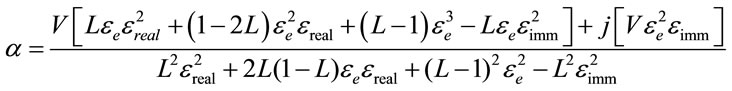 (8)
(8)
each term is studied and briefly reviewed in Table 2.
4. Sensitivity Analysis
In this Section we analyze the designed nanoparticle sensitivity properties in order to optimize the single inclusion for sensing applications.
Sensitivity is expressed in terms of the output variation (i.e., the wavelength shift Δλ) corresponding to a unit change of the input (i.e., the unit variation of either permittivity Δε or refractive index Δn). If the refractive index variation range is narrow enough, the input-output relation can be considered as a linear one. The sensitivity is commonly defined as:
 (9)
(9)
expressed in nm/RIU (Refractive Index Unit).
In Table 3, we report the sensitivity values for the individual inclusions considered in this paper. In particular, analytical, numerical and experimental values [23] of sensitivity are compared.
A test material surrounding the nanoparticle, with a varying refractive index n in the range 1 - 3, has been used.
5. Conclusions
This study investigated the potential role of non-spherical nanoparticles to be used for sensing applications. Different shapes of the nanostructure were considered, namely cube, nanorod and elliptic cylinder.
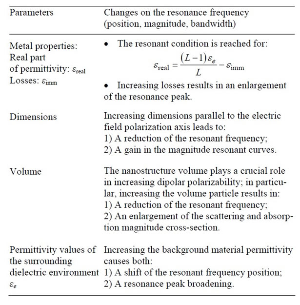
Table 2. The role of the geometrical parameters, metal properties and permittivity value of the dielectric environment on the nanoparticle resonant frequency.
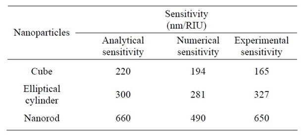
Table 3. Comparison of the sensitivity values for the inclusions considered.
In particular, new closed-form design formulas in order to describe the nanoparticle resonant behavior in terms of wavelength position, magnitude and bandwidth for absorption and scattering cross-section were developed. A good agreement among the proposed analytical model, the numerical values and the experimental ones present in literature was reached.
In addition, it was verified the possibility to use such nanoparticles as sensing platforms in the visible and infrared frequency regime. Exploiting the proposed analytical models, the effects of the geometrical and electromagnetic parameters on the particle resonant behavior were explored.
Analytical and full-wave results have validated and confirmed the high sensitivity properties of these structures.
Finally, the electromagnetic properties of the selected nanoparticles were compared with each other, in order to choose the structure that best suits specific sensing applications.
The employment of nanostructures grants for a reduction of the overall sensing platform size, and therefore, the biological volume required for sensing is reduced by several orders of magnitude.
REFERENCES
- A. Moores and F. Goettmann, “The Plasmon Band in Noble Metal Nanoparticles: An Introduction to Theory and Applications,” New Journal of Chemistry, Vol. 30, No. 8, 2006, pp. 1121-1132. doi:10.1039/b604038c
- J. B. Pendry, “Playing Tricks with Light,” Science, Vol. 285, No. 5434, 1999, pp. 1687-1688. doi:10.1126/science.285.5434.1687
- S. A. Maier, P. G. Kik, H. A. Atwater, S. Meltzer, E. Harel, B. E. Koel and A. G. Requicha, “Local Detection of Electromagnetic Energy Transport below the Diffraction Limit in Metal Nanoparticle Plasmon Waveguides,” Nature Materials, Vol. 2, No. 4, 2003, pp. 229-232. doi:10.1038/nmat852
- J. C. Riboh, A. J. Haes, A. D. McFarland, C. Ranjit and R. P. Van Duyne, “A Nanoscale Optical Biosensor: Real Time Immunoassay and Nanoparticle Adhesion,” The Journal of Physical Chemistry B, Vol. 107, No. 8, 2003, pp. 1772- 1780. doi:10.1021/jp022130v
- J. J. Storhoff, R. Elghanian, R. C. Mucic, C. A. Mirkin and R. L. Letsinger, “DNA Directed Synthesis of Binary Nanoparticle Network Materials,” Journal of American Chemical Society, Vol. 120, No. 48, 1998, pp. 12674- 12675. doi:10.1021/ja982721s
- E. M. Larsson, J. Alegret, M. Kall and D. S. Sutherland, “Sensing Characteristics of NIR localized Surface Plasmon Resonances in Gold Nanoring for Application as Ultrasensitive Biosensors,” Nano Letters, Vol. 5, No. 5, 2007, pp. 1256-1263. doi:10.1021/nl0701612
- R. Bukasov, T. A. Ali, P. Nordlander and J. S. ShumakerParry, “Probing the Plasmonic Near-Field of Gold Nanocrescent Antennas,” ACS Nano, Vol. 4, No. 11, 2010, pp. 6639-6650. doi:10.1021/nn101994t
- W. J. Galush, S. A. Shelby, M. J. Mulvihill, A. Tao, P. Yang and J. T. Groves, “A Nanocube Plasmonic Sensor for Molecular Binding on Membrane Surfaces,” Nano Letters, Vol. 9, No. 5, 2009, pp. 2077-2082. doi:10.1021/nl900513k
- N. L. Rosi and C. A. Mirkin, “Nanostructures in Biodiagnostics,” Chemical Review, Vol. 105, No. 4, 2005, pp. 1547-1562. doi:10.1021/cr030067f
- J. Chen, B. J. Wiley, H. Cang, D. Campbell, F. Saeki, L. Au, J. Lee, X. Li and Y. Xia, “Gold Nanocages: Engineering the Structures for Biomedical Applications,” Advanced Materials, Vol. 17, No. 18, 2005, pp. 2255-2261. doi:10.1002/adma.200500833
- M. J. Dukes, D. B. Peckys and N. de Jonge, “Correlative Fluorescence Microscopy and Scanning Transmission Electron Microscopy of Quantum-Dot-Labeled Proteins in Whole Cells in Liquid,” ACS Nano, Vol. 4, No. 7, 2010, pp. 4110-4116. doi:10.1021/nn1010232
- C. N. Ramachandra Rao, G. U. Kulkarni, P. J. Thomas and P. P. Edwards, “Metal Nanoparticles and Their Assemblies,” Chemical Society Reviews, Vol. 29, No. 1, 2000, pp. 27-35. doi:10.1039/a904518j
- X. Qian, X. H. Peng, D. O. Ansari, Q. Yin-Goen, G. Z. Chen, D. M. Shin, L. Yang, A. N. Young, M. D. Wang and S. Nie, “In Vivo Tumor Targeting and Spectroscopic Detection with Surface-Enhanced Raman Nanoparticle Tags,” Nature Biotechnology, Vol. 26, No. 1, 2008, pp. 83-90. doi:10.1038/nbt1377
- W. Cai, T. Gao, H. Hong and J. Sun, “Application of Gold Nanoparticles in Cancer Nanotechnology,” Nanotechnology, Science and Application, Vol. 1, 2008, pp. 17-32.
- P. B. Johnson and R. W. Christy, “Optical Constants of the Noble Metals,” Physical Review B, Vol. 6, No. 12, 1972, pp. 4370-4379. doi:10.1103/PhysRevB.6.4370
- CST Computer Simulation Technology. http://www.cst.com
- C. Bohren and D. Huffmann, “Absorption and Scattering of Light by Small Particles,” John Wiley, New York, 1983.
- A. Sihvola, “Electromagnetic Mixing Formulas and Applications,” The Institution of Engineering and Technology, London, 2008.
- J. G. Van Bladel, “Electromagnetic Fields,” John Wiley & Sons, Hoboken, 2007. doi:10.1002/047012458X
- H.-L. Wu, C.-H. Kuo and M. H. Huang, “Seed-Mediated Synthesis of Gold Nanocrystals with Systematic Shape Evolution from Cubic to Trisoctahedral and Rhombic Dodecahedral Structures,” Langmuir, Vol. 26, No. 14, 2010, pp. 12307-12313. doi:10.1021/la1015065
- M. Hu, J. Chen, Z. Y. Li, L. Au, G. V. Hartland, X. Li, M. Marquez and Y. Xia, “Gold nanostructures: Engineering Their Plasmonic Properties for Biomedical Applications,” Chemical Society Reviews, Vol. 35, No. 11, 2006, pp. 1084-1094. doi:10.1039/b517615h
- P. Hanarp, M. Käll and D. S. Sutherland, “Optical Properties of Short Range Ordered Arrays of Nanometer Gold Disks Prepared by Colloidal Lithography,” The Journal of Physical Chemistry B, Vol. 107, No. 24, 2003, pp. 5768- 5772. doi:10.1021/jp027562k
- T. Chung, S.-Y. Lee, E. Y. Song, H. Chun and B. Lee, “Plasmonic Nanostructures for Nano-Scale Bio-Sensing,” Sensors, Vol. 11, No. 11, 2011, pp. 10907-10929. doi:10.3390/s111110907