Open Journal of Metal
Vol.3 No.4(2013), Article ID:40764,7 pages DOI:10.4236/ojmetal.2013.34009
Optical Studies of Ag2O Thin Film Prepared by Electron Beam Evaporation Method
1Department of Physics, Sri Meenakshi Government College for Women, Madurai, India
2School of Physics, Madurai Kamaraj University, Madurai, India
Email: *sarosmgca@gmail.com
Copyright © 2013 Gandhimathinathan Saroja et al. This is an open access article distributed under the Creative Commons Attribution License, which permits unrestricted use, distribution, and reproduction in any medium, provided the original work is properly cited.
Received September 21, 2013; revised October 21, 2013; accepted October 28, 2013
Keywords: Silver Oxide; Thin Film; Extinction Coefficient
ABSTRACT
Silver oxide (Ag2O) thin films were deposited on glass substrates using electron beam gun evaporation techniques without oxygen atmosphere. The deposited films were post annealed at 100˚C, 150˚C, and 200˚C, respectively. The surface morphologies, structural and optical properties at different annealing temperatures were studied using scanning electron microscopy (SEM), X-ray diffraction (XRD), and ultra-violet-visible spectroscopy. The XRD results show that the intensity of (200) plane intensified as the annealing temperature increased from 100˚C to 200˚C. The XRD spectra reveal that the films are polycrystalline, having cubic structure irrespective of post annealing temperatures. The optical band gap of Ag2O thin films decreases from 1.716 eV to 1.559 eV as the annealing temperature increases from 100˚C to 200˚C.
1. Introduction
Silver has been valued throughout history for many of its properties that are useful to humans. It is used as a precious commodity in currencies, ornaments, jewellery, electrical contacts and photography. One of the most beneficial uses of silver has been as a potent antibacterial agent that is toxic to fungi, viruses and algae. Silver has long been used as a disinfectant; for example, the metal has been used in treating wounds and burns because of its broad-spectrum toxicity to bacteria as well as because of its reputation of limited toxicity to humans.
Development of new nanomaterials with metal nanoparticles (Ag, Au, Cu, Rh, Pd, etc.) deposited on glass surfaces, has gained much attention in material science because of expanding applications of such composites in optics, medical diagnostics, analytical chemistry, catalysis, photo catalysis etc. In this work we present improved photo-thermo chemical production of AgO and Ag2O3, metal functional films, as well as binary and ternary oxide composites via glass substrate assisted electron beam gun evaporation method with Ag nanoparticles (NPs) [1].
Argentous oxide is also described as silver (1) oxide or Ag2O with the 2 representing the number of silver atoms combining with each oxygen atom. Argentic oxide or silver (2) oxide is also known as plain silver oxide or silver peroxide. The peroxide here indicates that the compound contains more oxygen than usual.
Metal oxides in the Ag-O system, including Ag2O, AgO, Ag3O4and Ag2O3, constitute a fascinating group of inorganic materials [2]. Silver oxides crystallize in various types of crystal structures, leading to a variety of interesting physico chemical properties such as catalytic, electrochemical, electronic and optical properties. Therefore, silver oxide nanocrystals and thin films have been intensively pursued for promising applications as a catalyst for ethylene and methanol oxidation [3,4], as a sensor for the detection of carbon monoxide and ammonia [5-7], as photovoltaic materials [8-10], as important components in optical memories [11] and plasmon photonic devices [12], or as active cathode materials in silver oxide/zinc alkaline batteries [13,14]. The properties of silver oxide nanostructures and thin films are found to be vitally sensitive to the growth method and the experimental conditions applied.
Park et al. [15] reported that the occurred band was attributed to the localized state of oxygen vacancies in AgO cubic-like structure. A weak shoulder peak seen at 440 nm was the bluish green emission due to the presence of defects in the films. Without oxygen partial pressure at RT, the peak shifted to 618 nm attributed to blue emission due to the reduction of oxygen vacancies. Niederberger et al. [16] and Luo et al. [17] suggested that the blue emission was attributed to the band-to-band transition. The possible reason that sufficient oxygen is available in the sputter chamber leads to formation of stoichiometric Ag2O films as explained in EDAX analysis and the films have O/W ratio of 2.98 at oxygen partial pressure of Pascal.
2. Experimental
Electron gun evaporation technique is that one of the oldest techniques used for depositing thin films [18,19], which is still widely used in the laboratories and in industries for depositing 54 metals and metal alloys. The following sequential basic steps take place: 1) a vapour is generated by boiling or subliming a source material; 2) the vapour is transported from the source to the substrate; and 3) the vapour is condensed to a solid film on the substrate surface.
Thin films of Ag2O were prepared by EBE technique using a HINDHI-VAC vacuum unit (model: 12A4D) fitted with electron beam power supply (model: EBG-PS- 3K). Well degreased microscopic glass plates have been employed as the substrates in the present work. 500 mg of spectroscopically pure Ag2O (99.99%) was mixed well using a pestle and mortar. The mixture was pressed into pellets by hydraulic method to get pellet with a pressure of 500 kg/cm2, which was used as the source material for evaporation. The pellet was taken in a graphite crucible and kept in water cooled copper hearth of the electron gun. The pelletized Ag2O targets were heated by means of an electron beam collimated from the dc heated tungsten filament cathode. The surface of the Ag2O pellet was bombarded by 180˚ deflected electron beam with an accelerating voltage of 5 kV and a power density of ~1.5 kW/cm2. The evaporated species from Ag2O pellet were deposited as thin films on the substrates in a pressure of about 1 × 10⁻⁵ mbar. Each substrate was placed normal to the line of sight from the evaporation source at a polar angle to avoid shadow effects and also to obtain uniform deposition. The different preparation parameters such as source to substrate distance (15 cm) and partial pressure (10−5 mbar) have been varied and optimized for depositing uniform, well adherent and transparent films. The rate of evaporation (0.5 nm/s) was used to deposit all Ag2O films. The as deposited Ag2O films were annealed at 100˚C, 200˚C and 300˚C, respectively, to study the effect of annealing temperature on the structural, optical, and morphological properties.
The structural properties of Ag2O thin films were investigated using PAN analytical X-ray diffractometer with CuKα radiation at λ = 1.5406 Å. The X-ray diffraction (XRD) pattern was recorded in the range of 20 to 60 at a scanning rate of 5˚ min−1. Morphological studies were performed using scanning electron microscopy (SEM, Hitachi S-3400N, Japan). For the optical characterization, the transmittance and absorbance spectra of the Ag2O thin films were recorded using a UV-Vis spectrophotometer (Schimadzu 160A).
3. Results and Discussion
3.1. Structural Characterisation
Figure 1 shows the XRD pattern of Ag2O films annealed at 100˚C, 150˚C and 200˚C respectively.
The peak intensity at the (200) plane increased with an increase in annealing temperature. The intensification of the peak appearing at (200) plane indicates that the crystal quality of the Ag2O thin films improves with the increase in annealing temperature which is shown in Figure 2. The crystalline character of Ag2O is greatly enhanced with smaller width of the peaks [20]. The average grain size was calculated by Scherrer’s equation,
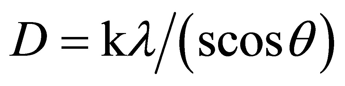 , (1)
, (1)
Where D is the grain size, β the full width at half maxima, θ is the angle of diffraction, and λ is the wavelength of X-ray (1 × 5409 Å).
The crystal lattice presents a series of parallel reflecting planes to the incident X-ray beam. The intensity of the reflected beam at certain angles will be maximum when the path difference between two reflected waves from two different crystal planes is an integral multiple of λ. This condition is termed as Bragg’s law and is given by,
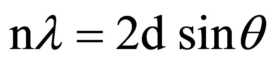 (2)
(2)
where, n is the order of diffraction, λ is the wavelength of X-rays, d is the spacing between consecutive parallel planes and θ is the glancing angle (or the complement of the angle of incidence) [21,22].
The lattice parameter c of the as-deposited room temperature Ag2O thin film is calculated using the formula for the hexagonal crystal structure. For the hexagonal crystal system, the lattice parameter c is related to d with the following equation
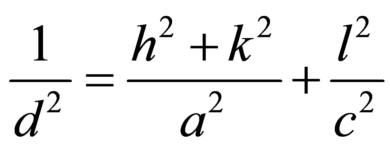 (3)
(3)
 (4)
(4)
Where h, k, and l are all integers, (hkl) is the lattice plane index, a and c are lattice constants, dhkl is distance between two consecutive planes (m = 1) with lattice plane index (hkl).
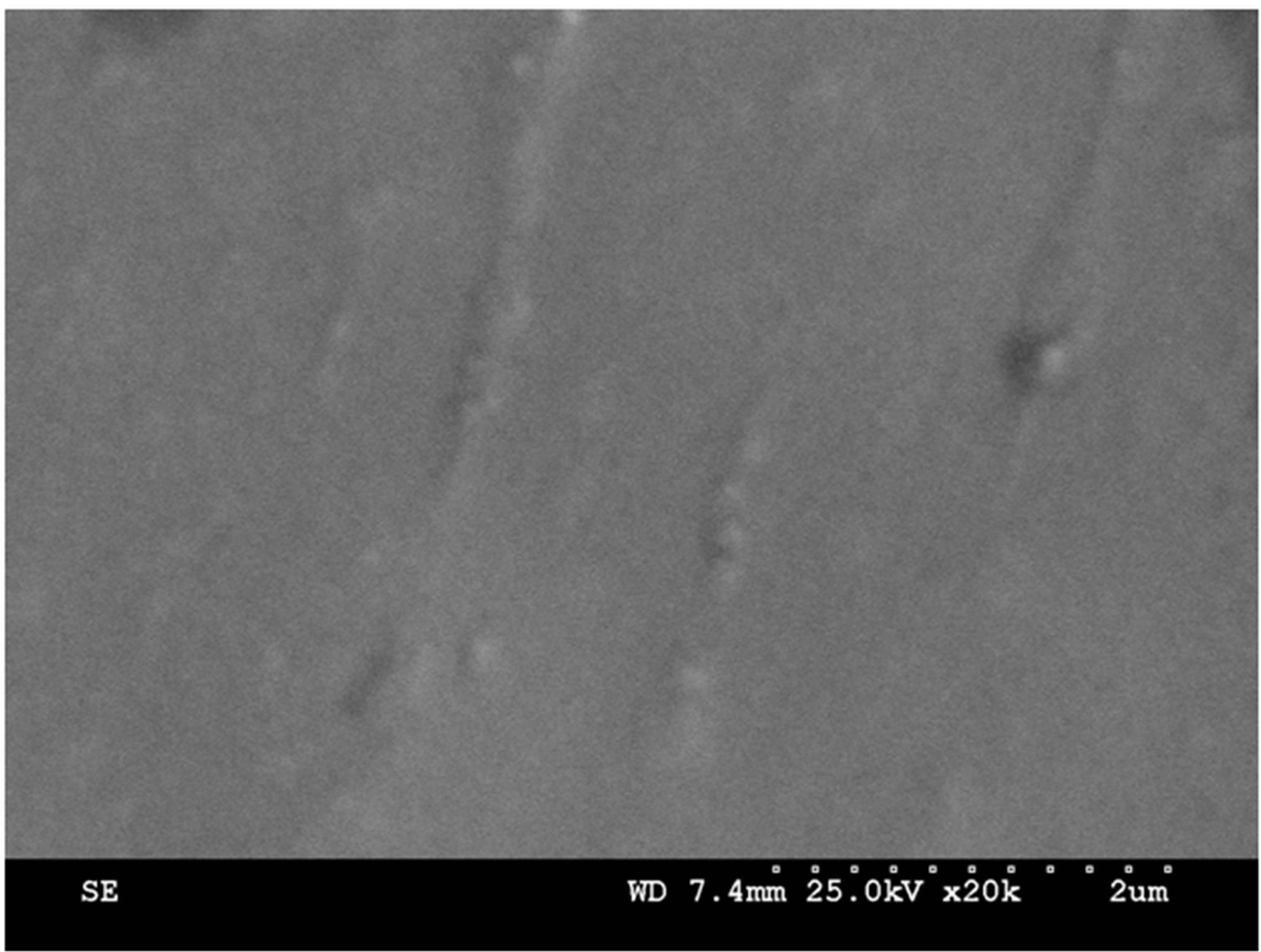
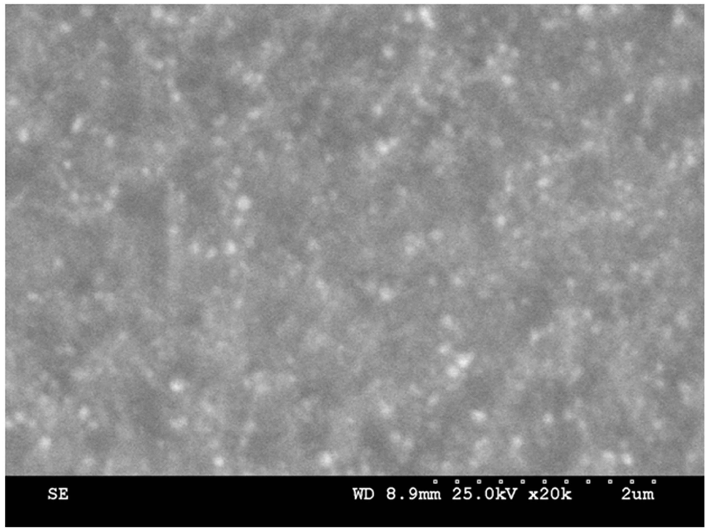
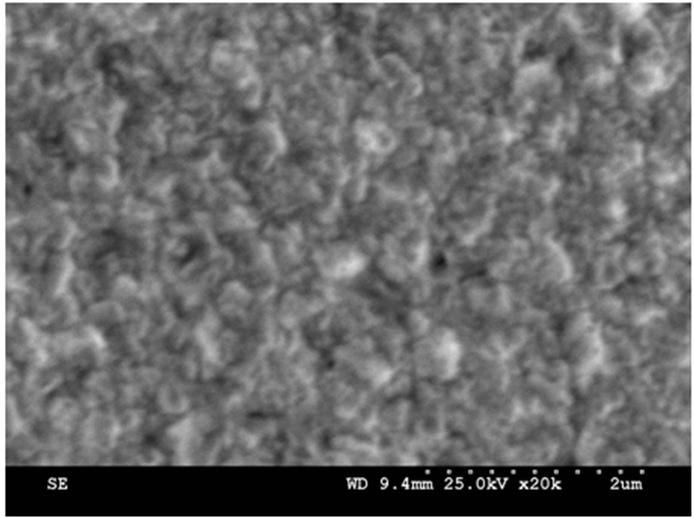
Figure 1. SEM Images of Ag2O thin film for different annealing temperatures.
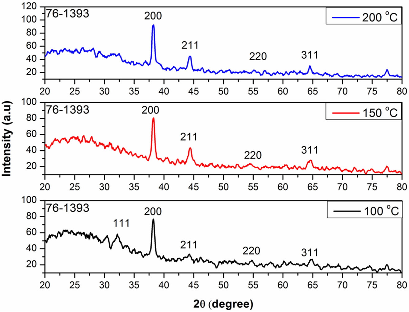
Figure 2. XRD pattern of Ag2O thin film for different annealing temperatures.
By using the standard formula [23], the values of strain (є), dislocation density (δ) and number of crystallites (N) were calculated.
The strain value ε can be evaluated by using the following relation:
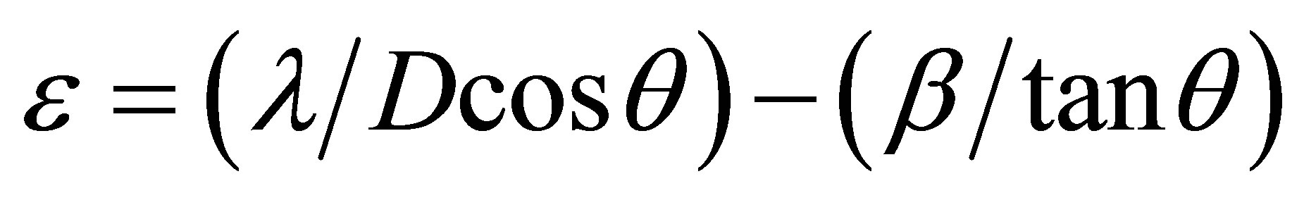 . (5)
. (5)
The dislocation density (δ) has been calculated by using the formula for thin films with cubic structure:
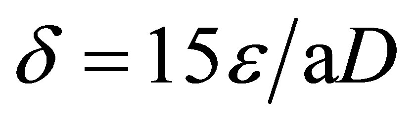 (6)
(6)
Using grain size (D) and film thickness (t), the number of crystallites N can be estimated using the relation
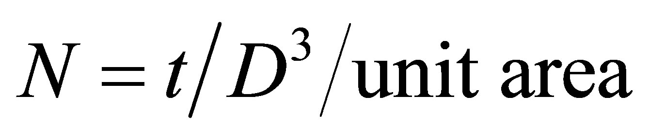 (7)
(7)
From the results of without oxygen atmosphere Ag2O thin film and different annealing effects of RT, 100˚C, 150˚C and 200˚C, we conclude that the process does improve the ordering of Ag2O structure; the optical properties of Ag2O thin films deposited without oxygen pressure can be greatly improved which is shown in Table 1. The annealing speed and annealing temperature are both important in improving the optical quality and crystallinity of the thin film. If the annealing time is constant (1 hr), the optical quality of the thin film cannot be greatly improved. If the annealing time is too high for example above 1 hr, the thin film will be broken because of the stress inside the thin film and gets peeled off from the substrate. Similarly, when the annealing temperature was used beyond 250˚C the films are non-adherent to the substrate. So we maintained the annealing temperature to a maximum of 200˚C only.
3.2. SEM Studies of Ag2O Thin Film
Figure 1 depicts the SEM images of the Ag2O thin films annealed at different temperatures. It was observed that as the annealing temperature increases from 100˚C to 150˚C, the film displays small particles on the surface of the film. Further increase in temperature from 150˚C to 200˚C, the films shows the accumulation of the Ag2O thin film. That accumulation may be attriburted due to the melting point of Ag2O.
3.3. Optical Studies
Figure 3 shows the optical absorbance spectra of Ag2O thin films annealed at 100˚C, 150˚C and 200˚C, respectively. The p-type conducting and reasonably high transparency, 62% at 550 nm, before and after annealing, the change of optical constants is very small. As observed in other work [24,25], there is an optical absorption occurring in the 1.5 - 1.6-eV photon-energy range for the Ag2O sample prepared by the chemical methods are depicted in Table 1. We did not see the strong optical absorption in this range, due to mixing of the microstructures of the sample prepared by the sputtering method. Through the annealing process, some of the Ag2O components in the as-deposited structure can be thermally decomposed into Ag2O and oxygen. The oxygen will react with a small amount of silver particles in the film. Such a chain reaction process may occur as: AgO + Ag → Ag2O.
Therefore, the annealing process will certainly improve the crystallization of the film, to cause a change of the optical properties, especially in the high-energy range.
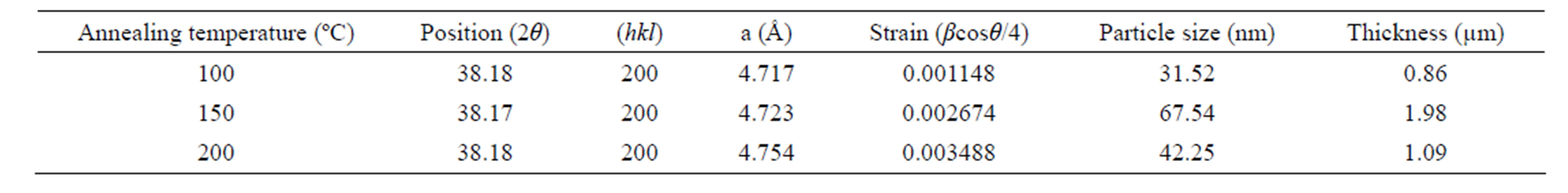
Table 1. XRD (Structural) parameters of Ag2O thin film deposited without oxygen atmosphere JCPDS card no 722108.
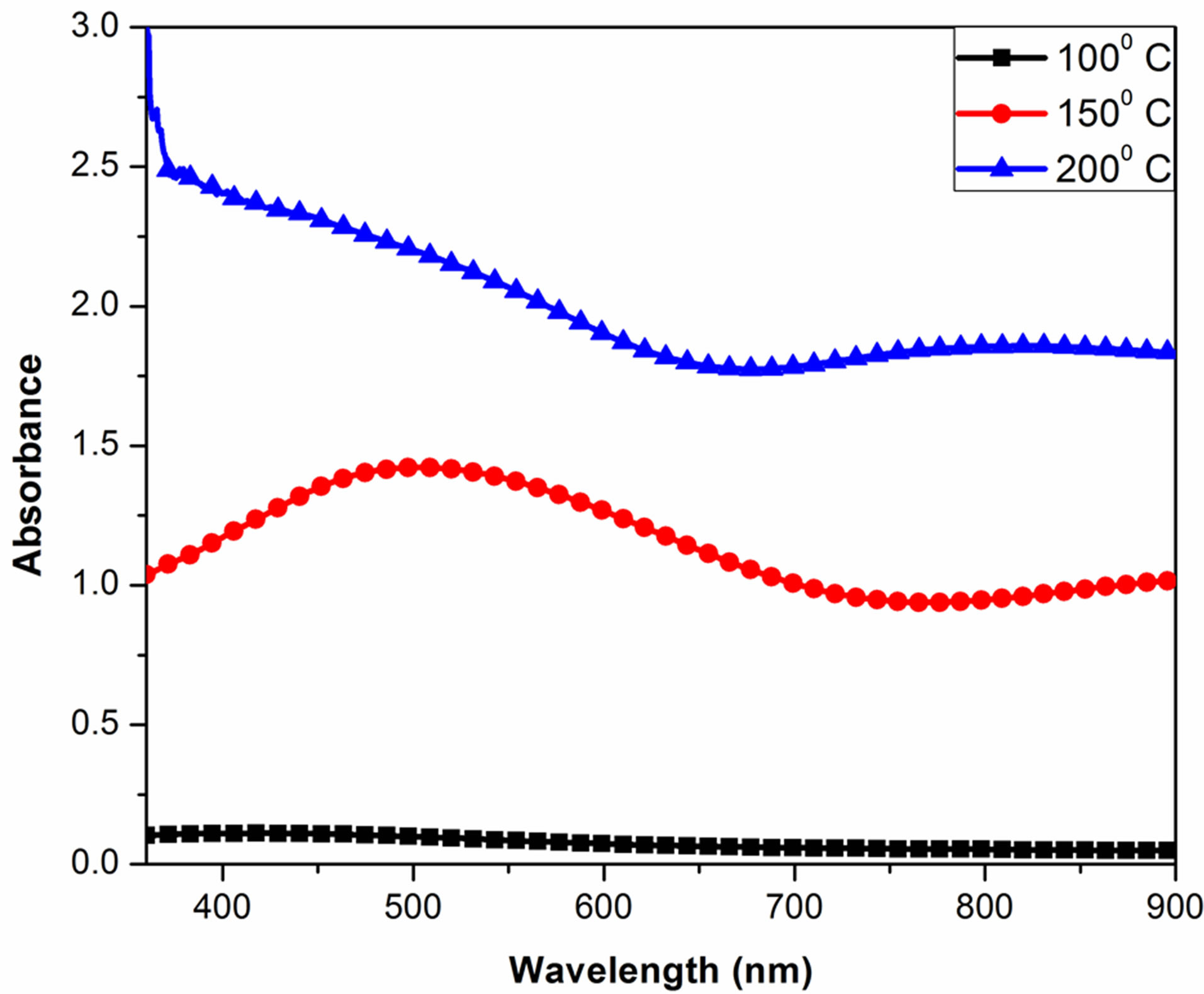
Figure 3. Absorbance curve of Ag2O thin film for different annealing temperatures.
Themicro-phase structure of the film, however, might still be a mixture of the amorphous and crystalline structures, depending on the sample preparation and annealing conditions. In the amorphous structure, Urbach tail [26] will induce a new density of states into the band gap, and thus the absorption spectra of Ag2O will be influenced.
To date, there is still a lack of detailed band-structure calculations to compare with the experimental data for Ag2O materials. For the direct or indirect interband optical transitions, the spectra of the optical absorption coefficient can be analyzed by using the following equations:
 ,
,
 where α is the absorption coefficient, A is a constant depending on details of the bandstructure, hγ is the photon energy, Eg is the absorption bandgap, m = 2 indicates an allowed indirect transition and m = 0.5 indicates an allowed direct transition. The optical bandgap was estimated by extrapolating the straight line of (
 )1/2 versus the photon energy as shown in Figure 4. The intercept of the tangent to the plot provides a good approximation of the bandgap energy of Ag2O thin films coated on glass substrate. The band gap of the Ag2O thin film annealed at 100˚C was 1.716 eV. This value gradually decreased to 1.6098 and 1.559 eV as the annealing temperature increased to 150˚C and 200˚C, respectively. The two linear sections shown in the curve indicate the allowed indirect
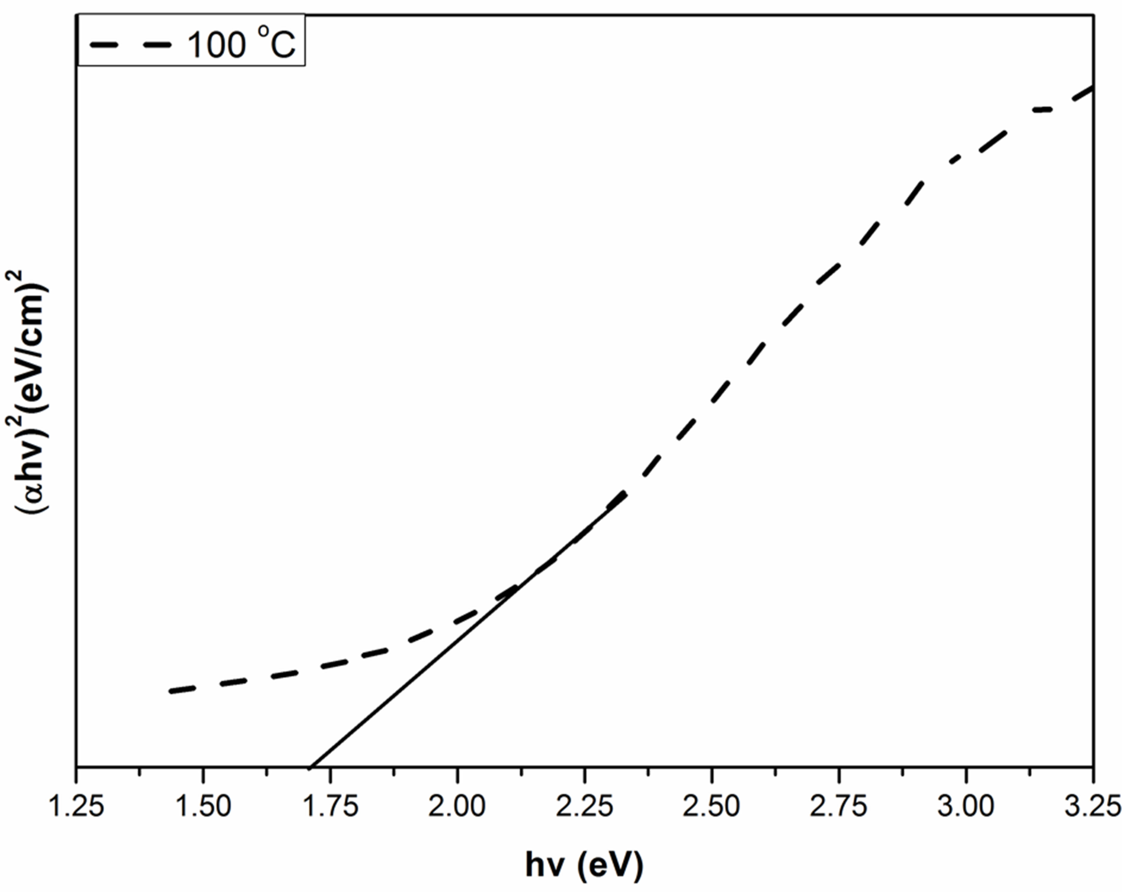
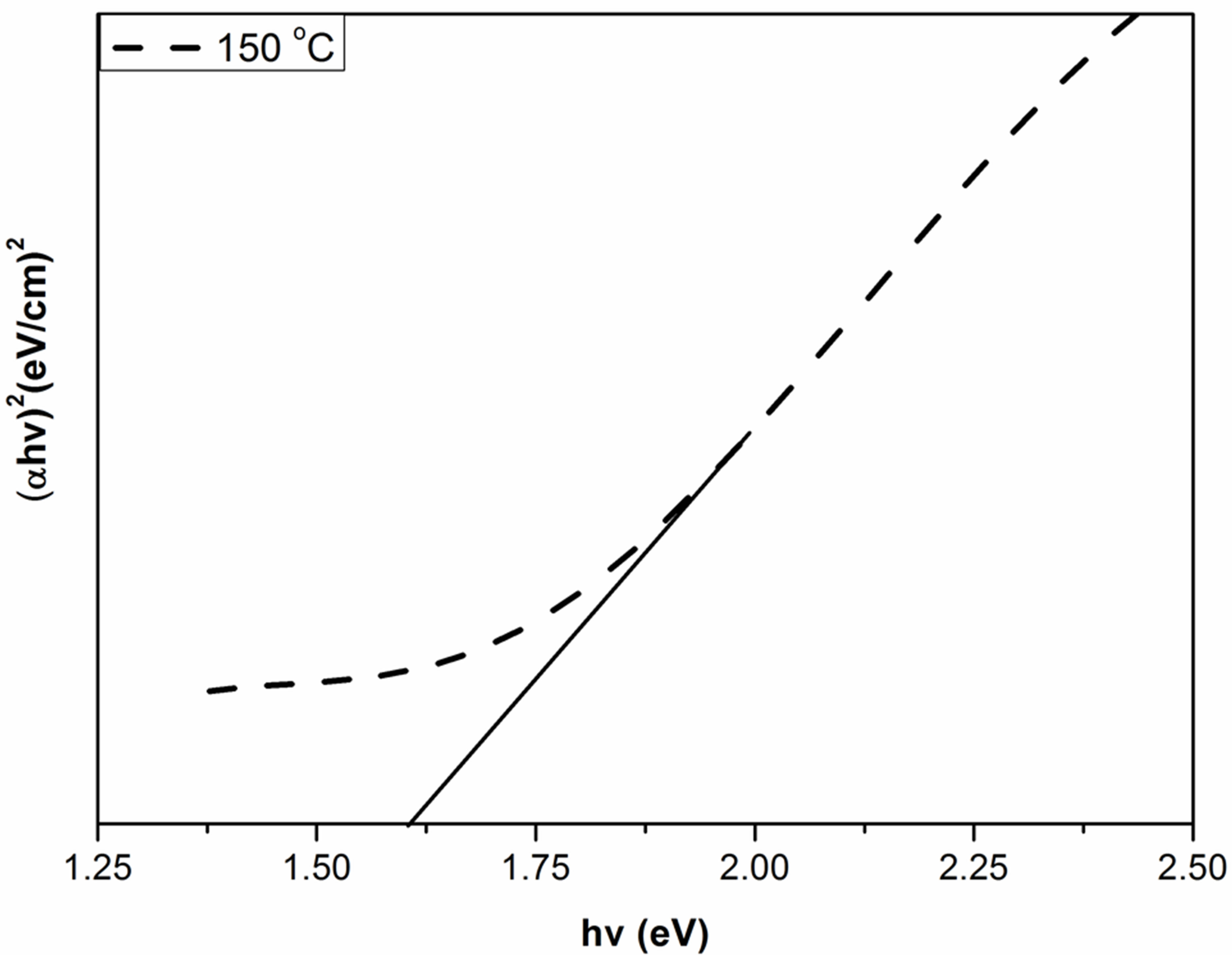
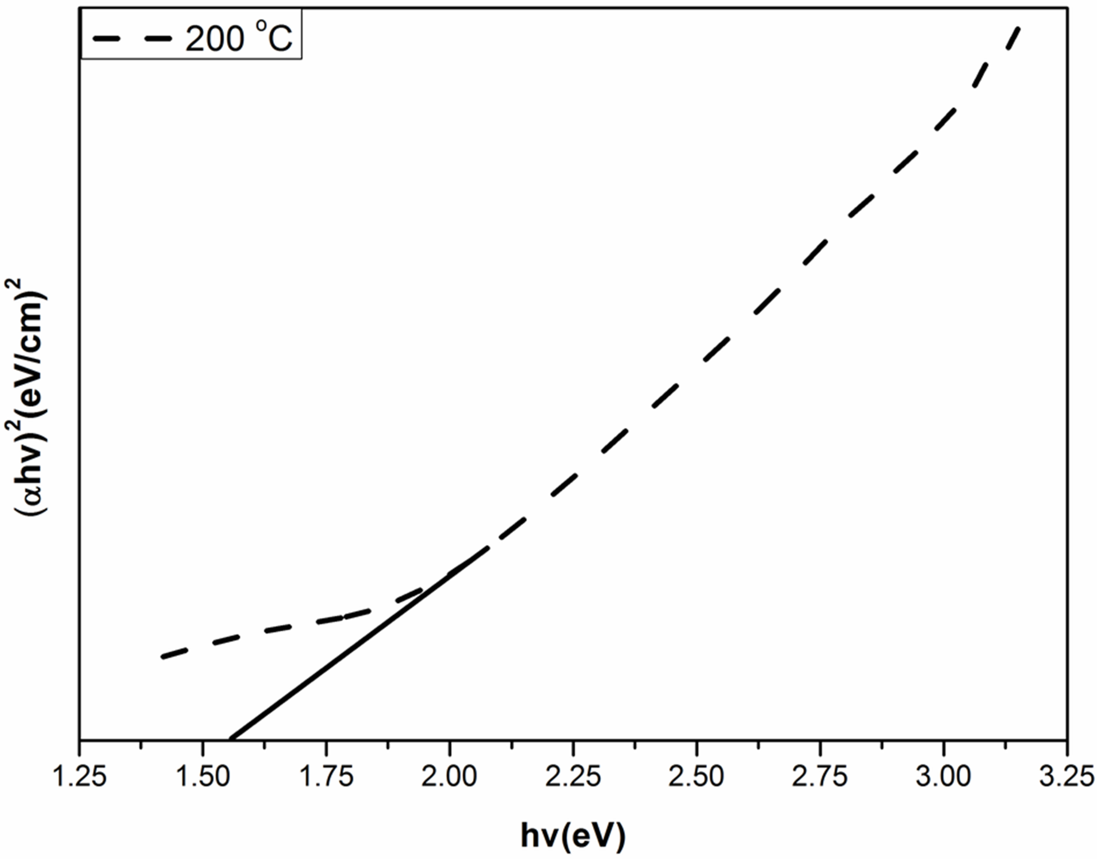
Figure 4. Band gap values of Ag2O thin films with different annealing temperature.
interband transitions.
The extrapolations of these linear sections yield band gaps: Eg100C = 1.716 eV, E150C = 1.6098 eV and E200C = 1.559 eV. The 0.066 eV-interband transitions tend to be attributed to the free-carrier response. In the data analysis of this work with the Tauc-Lorentz oscillator model, the value of Eg2 is close to Eg3 given in Figure 4. Eg2 is larger than the Ag2O bandgap of Eg1 eV. The optical band gap of the transmitting thin films calculated from the optical absorption spectra (using a Tauc plot) increases slightly (from 1.507 to 1.573 eV for AgO monoclinic structure table without the effect of oxygen pressure.
4. Conclusion
Ag2O thin films were successfully synthesized on glass substrate using ebeam evaporation technique. The effect of post annealing temperature on the morphological, structural, and optical properties of Ag2O thin films were investigated using X-ray diffraction, SEM and UV-Vis spectroscopy. The optical bandgap energy of the Ag2O thin films decreased as the annealing temperatures increased. The XRD intensity of (2 0 0) plane increased as annealing temperature increased.
REFERENCES
- J. F. Pierson and C. Rousselot, “Stability of Reactively Sputtered Silver Oxide Films,” Surface and Coatings Technology, Vol. 200, No. 1-4, 2005, pp. 276-279. http://dx.doi.org/10.1016/j.surfcoat.2005.02.005
- M. Pandiaraman and N. Soundararajan, “Micro-Raman Studies on Thermally Evaporated Ag2Se Thin Films,” Theoretical and Applied Physics, Vol. 6, 2012, p. 7. http://www.jtaphys.com/content/6/1/
- M. Bielmann, P. Schwaller, P. Ruffieux, O. Groning, L. Schlapbachand and P. Groning, “AgO Investigated by Photoelectron Spectroscopy: Evidence for Mixed Valence,” Physical Review B: Condensed Matter and Materials Physics, Vol. 65, No. 23, 2002, Article ID: 235431.
- N. Yamamoto, S. Tonomura, T. Matsuoka and H. Tsubomura, “The Effect of Reducing Gases on the Conductivities of Metal Oxide Semiconductors,” Japanese Journal of Applied Physics, Vol. 20, No. 4, 1981, pp. 721-726. http://dx.doi.org/10.1143/JJAP.20.721
- B. J. Murray, Q. Li, J. T. Newberg, E. J. Menke, J. C. Hemminger and R. M. Penner, “Shapeand Size-Selective Electrochemical Synthesis of Dispersed Silver(I) Oxide Colloids,” Nano Letters, Vol. 5, No. 11, 2005, pp. 2319-2324. http://dx.doi.org/10.1021/nl051834o
- B. J. Murray, Q. Li, J. T. Newberg, E. J. Menke, J. C. Hemminger and R. M. Penner, “Silver Oxide Microwires: Electrodeposition and Observation of Reversible Resistance Modulation upon Exposure to Ammonia Vapor,” Chemistry of Materials, Vol. 17, No. 26, 2005, pp. 6611-6618. http://dx.doi.org/10.1021/cm051647r
- B. J. Murray, J. T. Newberg, E. C. Walter, Q. Li, J. C. Hemminger and R. M. Penner, “Reversible Resistance Modulation in Mesoscopic Silver Wires Induced by Exposure to Amine Vapor,” Analytical Chemistry, Vol. 77, No. 16, 2005, pp. 5205-5214. http://dx.doi.org/10.1021/ac050636e
- E. Tselepis and E. Fortin, “Preparation and Photovoltaic Properties of Anodically Grown Ag2O Films,” Journal of Materials Science, Vol. 21, No. 3, 1986, pp. 985-988. http://dx.doi.org/10.1007/BF01117383
- Y. Ida, S. Watase, T. Shinagawa, M. Watanabe, M. Chigane, M. Inaba, A. Tasaka and M. Izaki, “Direct Electrodeposition of 1.46 eV Bandgap Silver(I) Oxide Semiconductor Films by Electrogenerated Acid,” Chemistry of Materials, Vol. 20, No. 4, 2008, pp. 1254-1256. http://dx.doi.org/10.1021/cm702865r
- B. E. Breyfogle, C. Hung, M. G. Shumsky and J. A. Switzer, “Electrodeposition of Silver(II) Oxide Films,” Journal of the Electrochemical Society, Vol. 143, No. 9, 1996, pp. 2741-2746. http://dx.doi.org/10.1149/1.1837101
- Y. Her, Y. Lan, W. Hsu and S. Y. Tsai, “Effect of Constituent Phases of Reactively Sputtered AgOx Film on Recording and Readout Mechanisms of Super-Resolution Near-Field Structure Disk,” Journal of Applied Physics, Vol. 96, No. 3, 2004, p. 1283. http://dx.doi.org/10.1063/1.1767978
- J. Tominaga, “The Application of Silver Oxide Thin Films to Plasmon Photonic Devices,” Journal of Physics: Condensed Matter, Vol. 15, No. 25, 2003, p. R1101. http://dx.doi.org/10.1088/0953-8984/15/25/201
- W. A. Parkhurst, S. Dallek and B. F. Larrick, “Thermogravimetry-Evolved Gas Analysis of Silver Oxide Cathode Material,” Journal of The Electrochemical Society, Vol. 131, No. 8, 1984, pp. 1739-1742. http://dx.doi.org/10.1149/1.2115952
- S. Dallek, W. A. West and B. F. Larrick, “Decomposition Kinetics of AgO Cathode Material by Thermogravimetry,” Journal of the Electrochemical Society, Vol. 133, No. 12, 1986, pp. 2451-2454. http://dx.doi.org/10.1149/1.2108448
- S. Park, H. Kim, C. Jin, and C. Lee, “Intense Ultraviolet Emission from Needle-Like WO3 Nanostructures Synthesized by Noncatalytic Thermal Evaporation,” Nanoscale Research Letters, Vol. 6, No. 1, 2011, p. 451. http://dx.doi.org/10.1186/1556-276X-6-451
- M. Niederberger, M. H. Bartl and G. D. Stucky, “Benzyl Alcohol and Transition Metal Chlorides as a Versatile Reaction System for the Nonaqueous and Low-Temperature Synthesis of Crystalline Nano-Objects with Controlled Dimensionality,” Journal of the American Chemical Society, Vol. 124, No. 46, 2002, pp. 13642-13643. http://dx.doi.org/10.1021/ja027115i
- J. Y. Luo, F. L. Zhao, L. Gong et al., “Ultraviolet-Visible Emission from Three-Dimensional WO3-x Nanowire Networks,” Applied Physics Letters, Vol. 91, No. 9, 2007, pp. 093124-1-093124-3
- L. I. Maissel and R. Clang, “Handbook of Thin Film Technology,” McGraw-Hill, New York, 1970.
- R. F. Bunshah, “Deposition Technologies for Films and Coatings: Developments and Applications,” Noyes Publications, Park Ridge, 1982.
- J. Wang, V. Sallet, F. Jomard, A. M. Rego, E. Elamurugu, R. Martins and E. Fortunato, “Influence of Substrate Temperature on N-Doped ZnO Films Deposited by RF Magnetron Sputtering,” Thin Solid Films, Vol. 515, No. 24, 2007, pp. 8785-8788. http://dx.doi.org/10.1016/j.tsf.2007.03.061
- C. Vijayan, M. Pandiaraman, N. Soundararajan, R. Chandramohan, V. Dhanasekaran, K. Sundaram, T. Mahalingam and A John Peter, “Structural and Optical Properties of Ag2SeTe Nano Thin Films Prepared by Thermal Evaporation,” Journal of Materials Science: Materials in Electronics, Vol. 22, No. 5, 2011, pp. 545-550.
- M. Erol, Y. Han, S. K. Stanley, C. M. Stafford, H. Du and S. Sukhishvili, “SERS Not to Be Taken for Granted in the Presence of Oxygen,” Journal of the American Chemical Society, Vol. 131, No. 22, 2009, pp. 7480-7481. http://dx.doi.org/10.1021/ja807458x
- Y. Hoshi and T. Kiyomura, “ITO Thin Films Deposited at Low Temperatures Using a Kinetic Energy Controlled Sputter-Deposition Technique,” Thin Solid Films, Vol. 411, No. 1, 2002, pp. 36-41. http://dx.doi.org/10.1016/S0040-6090(02)00170-0
- A. K. Chawla, S. Singhal, H. O. Gupta and R. Chandra, “Effect of Sputtering Gas on Structural and Optical Properties of Nanocrystalline Tungsten Oxide Films,” Thin Solid Films, Vol. 517, No. 3, 2008, pp. 1042-1046. http://dx.doi.org/10.1016/j.tsf.2008.06.068
- R. Swanepoel, “Determination of the Thickness and Optical Constants of Amorphous Silicon,” Journal of Physics E, Vol. 16, No. 12, 1983, p. 1214.
- B. Baloukas, J. M. Lamarre and L. Martinu, “Electrochromic Interference Filters Fabricated from Dense and Porous Tungsten Oxide Films,” Solar Energy Materials and Solar Cells, Vol. 95, No. 3, 2011, pp. 807-815. http://dx.doi.org/10.1016/j.solmat.2010.10.026
NOTES
*Corresponding author.