Journal of Materials Science and Chemical Engineering
Vol.05 No.09(2017), Article ID:78615,9 pages
10.4236/msce.2017.59001
Investigation of Carrier Conduction Mechanism over InAs/InP Quantum Dashes and InAs/GaAs Quantum Dots Based p-i-n Laser Heterostructures
Neslihan Ayarcı Kuruoğlu, Orhan Özdemir, Kutsal Bozkurt
Department of Physics, Faculty of Science and Letters, Yıldız Technical University, Istanbul, Turkey

Copyright © 2017 by authors and Scientific Research Publishing Inc.
This work is licensed under the Creative Commons Attribution International License (CC BY 4.0).
http://creativecommons.org/licenses/by/4.0/


Received: July 27, 2017; Accepted: August 19, 2017; Published: August 22, 2017
ABSTRACT
Charge transfer characteristics of the long wavelength semiconductor laser structures, containing quantum dot layers (QDs), were investigated by means of temperature dependent current-voltage and electroluminescence measurements over InAs/InP, and InAs/GaAs based p-i-n structures. In InAs/InP elongated QDs (QDashes) structure, injected carriers were tunneled from the quantum well into QDashes through a thin barrier and subsequently recombined within QDashes. Meanwhile, for InAs/GaAs structure, tunneling kind transport was exhibited in both forward and reverse bias voltage directions. The onset of light took place when the forward bias exceeded 1.3 V (3 V) for InAs/InP (InAs/GaAs) p-i-n structure through electroluminescence measurements. The peak value of emitted laser light for InAs/InP QDashes and InAs/GaAs QDs occurred in 1.55 µm and 1.3 µm, respectively.
Keywords:
Long Wavelength Laser Diode, Quantum Dots, Quantum Dashes, Electroluminescence, Temperature Dependent Currentdensity-Voltage Characteristics

1. Introduction
III-V semiconductor low dimensional structures are attractive for optoelectronic devices, including laser diodes and infrared photodetectors [1] - [6] . The semiconductor quantum dots/quantum dashes (QDs) devices have a lower threshold current density, with a higher gain, and higher thermal stability because of energy confinement compared to bulk and quantum well lasers [4] . InAs/GaAs-based QDs devices emit a laser light at 1.3 µm wavelength [7] [8] [9] , while InAs/InP-based QDs devices allow a laser emission in the 1.4 to 1.6 µm wavelength range [2] [3] [4] [5] [6] .
Therefore, the charge transport properties are essential for the dynamic of a high-speed semiconductor laser [10] [11] . Nagarajan et al. discussed that the main limitation for laser structures was the charge transfer mechanism [10] . The discussion was carried out through optical and electrical measurement. Optical properties are found out by electroluminescence (EL) measurement for the analysis of optical properties [12] [13] [14] while the electrical characteristic of these structures is determined using current density-voltage (J-V) measurements [15] [16] [17] [18] . Furthermore, the properties of the present structures in the literature [4] [19] [20] are studied through various optical spectroscopy techniques such as photoluminescence (PL), photoreflectance (PR), and photoluminescence excitation (PLE) to derive the energies of the optical transitions in the system and to get insight of the carrier transfer. In this work, carrier transfer characteristics are investigated through current-voltage and electroluminescence measurements. In brief, carrier transportation properties are clarified in electrical stimulus rather than optical one. Additionally, the scheme of the present structures (given as inset of Figure 1 and Figure 2) is constructed by means of PL, PLE studies. It was observed that in InAs/InP QDashes structured carriers were first tunneled from the quantum well into QDashes in InAs/InP and then recombine within QDashes to emit a long wavelength laser light at 1.55 µm while in InAs/GaAs QDs, the tunneling transport of carriers was the governed conduction mechanism in the range of examined bias voltages.
2. Experiment Methods
State of the art device quality InAs/InP-based QDashes―elongated quantum dots- devices were grown by gas source molecular beam epitaxy on S-doped (100) InP wafers. The schematic structure was shown in the inset of Figure 1. Nine nominally undoped InAs QDashes layers have been stacked within a standard In GaAsP separate confinement heterostructure for increased modal gain. The nominal thickness of the InAs layer to achieve 1.55 µm emission is about 2 nm. P-type and n-type doped InP cladding layers were used for light confinement, which results in a p-i-n diode. On the other hand, InAs/GaAs-based QDs was grown by a molecular beam epitaxy on a semi-insulating GaAs (0 0 1) substrate. The schematic structure was shown in the inset of Figure 2. Nine InAs QDs layers have stack within In GaAsP. P-type and n-type doped Al0.85 Ga0.15 As cladding layers were used for light confinement. The whole structure was capped with 10 nm of GaAs. InAs/GaAs QDs and InAs/InP QDashes p-i-n laser heterostructure were studied using current density-voltage measurements in the range of 295 to 400 K. The current voltage measurements were carried out using a Keithley 2400 voltage/current source meter and Lake Shore 334 temperature controller. The EL measurements were performed using Keithley 2400 voltage/current source meter, equipped with an Oriel Cornerstone 260 monochromator and InGaAs photodiode, produced by ThorLabs. The emitted laser light from p-i-n structures was collected in the monochromator by using lenses. At the rear slit of the monochromator, InGaAs photodiode was used to detect the wavelength dependence of emitted light.
3. Result and Discussion
SEM images of the long wavelength laser heterostructure in the p-i-n diode were presented in Figure 3, demonstrating good morphology. For the electrical characteristics, the temperature dependent J-V measurement was performed in the range of 295 to 400 K to investigate the carrier conduction mechanism. The results of J-V measurement of InAs/GaAs QDs and InAs/InP based QDashes laser heterostructure were shown in Figure 1 and Figure 2, respectively. These figures showed an increase in the magnitude of current density with increasing temperature.
To elucidate the carrier conduction mechanism(s), a general diode equation is fitted, and the results are investigated in terms of activation energy (EA) of the saturation current (I0) and temperature dependence of the exponential factor (A) by performing temperature dependent current density-voltage measurement. In this context, the current density-voltage relation in the forward directions is expressed as [21] ,
 , (1)
, (1)

Figure 1. Temperature dependent dark J-V curves in forward/reverse direction on InAs/ InP quantum dashes. The inset shows the schematic band diagram of the structure.
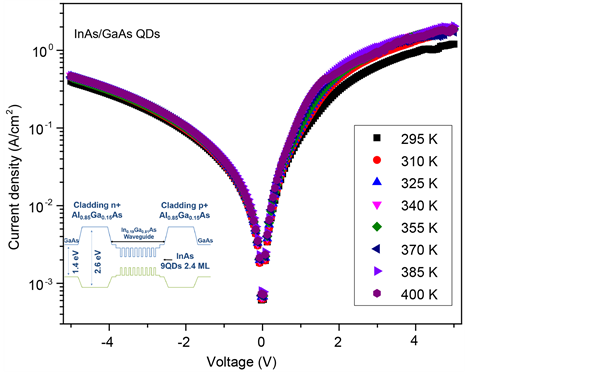
Figure 2. Temperature dependent dark J-V curves in forward/reverse direction on InAs/ GaAs QDs. The inset shows the schematic band diagram of the structure.

Figure 3. The SEM picture (a)-(b) of InAs/InP based QDashes and (c)-(d) InAs/GaAs QDs laser heterostructure.
where V is applied voltage. Dark saturation current density is given by
 (2)
(2)
with
 , (3)
, (3)
where k is Boltzmann’s constant, T is the absolute temperature in Kelvin, q is electron charge, and n is ideality factor.
In reverse direction, reverse current density-reverse bias followed the expression,
 (4)
(4)
with
 , (5)
, (5)
where Vbi is built-in voltage, VR is applied voltage in reverse bias, b is temperature independent exponent, and Jrev,0(T) is dark saturation current density in reverse bias, and EA,rev is reverse bias activation energy.
For QDashes based p-i-n laser heterostructure, the forward J-V characteristic manifested two distinct behaviors depending on the bias range (VF < 0.2 V and 0.2 < VF < 0.6 V). From the slopes of Arrhenius plots of ln J0vs. T−1 and Avs. T−1 variations, EA was deduced as 0.4 eV, and A was independent of temperature (Figure 4). Therefore, dominant conduction mechanism was the tunneling type. For the bias range of 0.2 < VF < 0.6 V, EA and n were determined as 0.4 eV and 2, respectively. Also, Arrhenius plot of the reverse current density versus reciprocal of temperature at constant bias voltages, resulting activation energy as 0.4 eV, like in forward direction. Both temperature independence of A together with the same activation energy in forward and reverse bias voltages in dictated tunneling of carrier conduction and followed by recombination/generation current flow once the bias voltage exceeded 0.2 V.
Similarly, InAs/GaAs Quantum Dot based p-i-n structure was analyzed (Figure 5). Remarkably, rather than two kinds of carrier conduction mechanism, tunneling type conduction was manifested for bias voltage range in reverse/ forward direction.
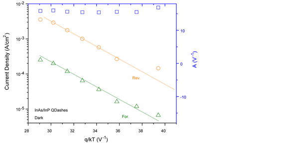
Figure 4. The activation energy of InAs/InP QDashes in forward/reverse direction and A versus q/kT to obtain ideality factor from the slope of semi log current density bias variation.
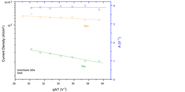
Figure 5. The activation energy of InAs/GaAs QDs in forward/reverse direction and A versus q/kT to obtain ideality factor from the slope of semi log current density bias variation.
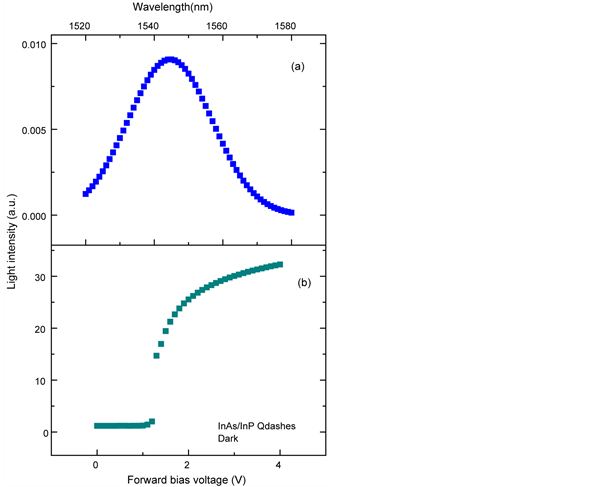
Figure 6. (a) Wavelength dependence of light produced from InAs/InP QDashes at room temperature; (b) EL measurement on this structure.

Figure 7. (a) Wavelength dependence of light generated from InAs/GaAs QDs at room temperature; (b) EL measurement on this structure.
Furthermore, when the junctions entered the space charge limited region (VF > 1 V for InAs/InP Quantum dash and VF > 2 V for InAs/GaAs Quantum Dot), the laser light was observed (Figure 6(b) and Figure 7(b)). As shown in there, the onset of light took place when the bias exceeded 1.3 V for InAs/InP Quantum dash while 3 V for InAs/GaAs p-i-n structure. Moreover, the intensity of light grew with the increase in bias voltages and finally saturated for both structures. Figure 6(a) and Figure 7(a) showed wavelength dependence of light produced from InAs/InP QDashes and InAs/GaAs QDs in which the peak value of emitted laser light took place in 1.55 µm and 1.3 µm, as expected.
4. Conclusion
Long wavelength laser diodes in the p-i-n structure were investigated by temperature dependent current density-voltage measurements. Tunneling kind carrier conduction mechanism was identified for InAs/GaAs-based p-i-n structure for whole bias voltages, whereas transition of tunneling type to recombination/gen- eration kind carrier conduction was discerned in InAs/InP-based p-i-n laser diode. As to the EL measurements, laser light emerged for both structures, peaking at 1.55 µm and 1.3 µm, respectively.
Acknowledgements
The authors are grateful to Laboratory for Photonics and Nanostructures (LPN), CNRS for the sample production and Prof. Dr. Abderrahim Ramdaneand his co- workers.
Cite this paper
Kuruoğlu, N.A., Özdemir, O. and Bozkurt, K. (2017) Investigation of Carrier Conduction Mechanism over InAs/InP Quantum Dashes and InAs/ GaAs Quantum Dots Based p-i-n Laser Heterostructures. Journal of Materials Science and Chemical Engineering, 5, 1-9. https://doi.org/10.4236/msce.2017.59001
References
- 1. Arakawa, Y. and Sakaki, H. (1982) Multidimensional Quantum Well Laser and Tem-perature Dependence of Its Threshold Current. Applied Physics Letters, 40, 939-941.
https://doi.org/10.1063/1.92959 - 2. Vusirikala, V., Saini, S., Bartolo, R., Agarwala, S., Whaley, R., Johnson, F., Stone, D. and Dagenais, M. (1997) 1.55μm InGaAsP-InP Laser Arrays with Integrated-Mode Expanders Fabricated Using a Single Epitaxial Growth. IEEE Journal of Selected Topics in Quantum Electronics, 3, 1332-1343.
https://doi.org/10.1109/2944.658787 - 3. Doussiere, P., Garabedian, P., Graver, C., Derouin, E., Gaumont-Goarin, E., Michaud, G. and Meilleur, R. (1994) Tapered Active Stripe for 1.5 μm InGaAsP/InP Strained Multiple Quantum Well Lasers with Reduced Beam Divergence. Applied Physics Letters, 64, 539.
https://doi.org/10.1063/1.111096 - 4. Lelarge, F., Dagens, B., Renaudier, J., Brenot, R., Accard, A., Van Dijk, F., Make, D., Le Gouezigou, O., Provost, J.G., Poingt, F., Landreau, J., Drisse, O., Derouin, E., Rousseau, B., Pommereau, F. and Duan, G.H. (2007) Recent Advances on InAs/InP Quantum Dash Based Semiconductor Lasers and Optical Amplifiers Operating at 1.55 μm. IEEE Journal on Selected Topics in Quantum Electronics, 13, 111-123.
https://doi.org/10.1109/JSTQE.2006.887154 - 5. Merghem, K., Akrout, A., Martinez, A., Moreau, G., Tourrenc, J.-P., Lelarge, F., Van Dijk, F., Duan, G.-H., Aubin, G. and Ramdane, A. (2008) Short Pulse Generation using a Passively Mode Locked Single InGaAsP/InP Quantum Well Laser. Optics Express, 16, 10675.
https://doi.org/10.1364/OE.16.010675 - 6. Duan, G.-H., Shen, A., Akrout, A., Dijk, F.V., Lelarge, F., Pommereau, F., LeGouezigou, O., Provost, J.-G., Gariah, H., Blache, F., Mallecot, F., Merghem, K., Martinez A. and Ramdane, A. (2009) High Performance InP Based Quantum Dash Semiconductor Mode-Locked Lasers for Optical Communications. Bell Labs Technical Journal, 14, 63-84.
https://doi.org/10.1002/bltj.20388 - 7. Saint-Girons, G., Mereuta, A., Gérard, J.M., Ramdane, A. and Sagnes, I. (2000) 1.3 μm Electroluminescenceof LP-MOVPE Grown InAs/GaAs Quantum Dots, and Influence of the Re-Growth Temperature on the Spectral Response. Materials Science, and Engi-neering: B, 78, 145-147.
https://doi.org/10.1016/S0921-5107(00)00542-0 - 8. Dagens, B., Martinez, A., Provost, J.-G., Make, D., Le Gouezigou, O., Ferlazzo, L., Merghem, K., Lema ître, A., Ramdane, A. and Thedrez, B. (2006) High Extinction Ratio and High-Temperature 2.5-Gb/s Floor-Free 1.3 μm Transmission with a Directly Modulated Quantum Dot Laser. IEEE Photonics Technology Letters, 18, 589-591.
https://doi.org/10.1109/LPT.2006.870189 - 9. Tanabe, K., Watanabe, K. and Arakawa, Y. (2012) 1.3 μm InAs/GaAs Quantum Dot Lasers on Si rib Structures with Current Injection across Direct-Bonded GaAs/Si Hetero-interfaces. Optics Express, 20, B315-321.
https://doi.org/10.1364/OE.20.00B315 - 10. Nagarajan, R., Ishikawa, M., Fukushima, T., Geels, R.S. and Bowers, J.E. (1992) High Speed Quantum-Well Lasers and Carrier Transport Effects. IEEE Journal of Quantum Electronics, 28, 1990-2008.
https://doi.org/10.1109/3.159508 - 11. Burrows, P.E., Shen, Z., Bulovic, V., McCarty, D.M., Forrest, S.R., Cronin, J.A. and Thompson, M.E. (1996) Relationship between Electroluminescence and Current Transport in Organic Heterojunction Light-Emitting Devices. Journal of Applied Physics, 79, 7991-8006.
https://doi.org/10.1063/1.362350 - 12. Veselinov, K., Grillot,F., Miska,P., Homeyer, E., Caroff,P., Platz, C., Even, J., Marie, X., Dehaese, O., Loualiche, S. and Ramdane, A. (2006) Carrier Dynamics and Saturation Effect in (113)B InAs/InP Quantum Dot Lasers. Optical and Quantum Electronics, 38, 369-379.
https://doi.org/10.1007/s11082-006-0037-2 - 13. Caroff, P., Paranthoen, C., Platz, C., Dehaese, O., Folliot, H., Bertru, N., Labbé, C., Piron, R., Homeyer, E., Le Corre, A. and Loualiche, S. (2005) High-Gain and Low- Threshold InAs Quantum-Dot Lasers on InP. Applied Physics Letters, 87, Article ID: 243107.
https://doi.org/10.1063/1.2146063 - 14. Bozkurt, K. (2016) Electroluminescence Study of InP/InGaAsP/InAs/InP P-I-N Laser Heterostructure. Sigma Journal of Engineering and Natural Sciences, 34, 255-259.
- 15. Lau, P.-K. and Makino, T. (1998) Current-Voltage Characteristics of Long Wavelength Quantum-Well Laser Diodes. Journal of Applied Physics, 83, 1183.
https://doi.org/10.1063/1.366903 - 16. Li, S.G., Gong, Q., Cao, C.F., Wang, X.Z., Yue, L., Wang, H.L. and Wang, Y. (2012) Meas-urements of I-V Characteristics in InAs/InP Quantum Dot Laser Diode. Journal of Modern Optics, 59, 1695-1699.
https://doi.org/10.1080/09500340.2012.737480 - 17. Ayarci, N., Özdemir, O., Bozkurt, K., Ramdane, A., Belahsene, S. and Martinez A. (2016) Discrimination of Carrier Conduction Mechanisms of InP/InGaAsP/ InAs/InP Laser Structure through Measurements. IEEE Transactions on Electron Devices, 63, 1866-1870.
https://doi.org/10.1109/TED.2016.2545411 - 18. Yang, W., Li, D., He, J., Wang, C. and Hu, X. (2014) Temperature-Dependent AC Cur-rent-Voltage-Capacitance Characteristics of GaN-Based Light-Emitting Diodes under High Forward Bias. Physica Status Solidi, 11, 714-717.
https://doi.org/10.1002/pssc.201300434 - 19. Saint-Girons, G., Patriarche, G., Largeau, L., Coelho, J., Mereuta, A., Gerard, J.M. and Sagnes, I. (2002) Metal-Organic Vapor-Phase Epitaxy of Defect-Free InGaAs/GaAs Quantum Dots Emitting around 1.3 μm. Journal of Crystal Growth, 235, 89-94.
- 20. Rudno-Rudziński, W., Sek, G., Ryczko, K., Syperek, M., Misiewicz, J., Semenova, E.S., Lemaitre, A. and Ramdane, A. (2009) Room Temperature Free Carrier Tunneling in Dilute Nitride Based Quantum Well-Quantum Dot Tunnel Injection System for 1.3 μm. Applied Physics Letters, 94, Article ID: 171906.
https://doi.org/10.1063/1.3122935 - 21. Sze, S.M. (1981) Physics of Semiconductor Devices. 2nd Edition, John Wiley & Sons, New York.