Journal of Electronics Cooling and Thermal Control
Vol.1 No.3(2011), Article ID:9223,9 pages DOI:10.4236/jectc.2011.13004
Effect of Heat Extraction by Metal Lines and Two Sided Cooling on Temperatures in Organic Light Emitting Diode Based Devices
Department of Materials Science and Engineering, Samtel Center for Display Technologies, Indian Institute of Technology, Kanpur, India
E-mail: saboo@iitk.ac.in
Received September 12, 2011; revised November 15, 2011; accepted November 25, 2011
Keywords: Cooling, Displays, OLED
Abstract
Only a 10 K rise in temperature of organic light emitting diode (OLED) can lower its lifetime by more than 50% and cause other performance deterioration. We have performed two dimensional heat transport analysis and calculated temperatures in an OLED panel. The panel temperatures can easily rise in excess of 10 K. Further we have investigated loss of heat through the metal lines for the extent by which they could lower the temperature. However, this method leads to gradients in temperature which could in turn cause inhomogeneities in a display. But, in lighting panels, it will be feasible to cool the devices from both the sides, which is shown to have a significant impact. The thermal transport model presented here for displays is more extensive in its approach and hence likely to provide more accurate results.
1. Introduction
Organic light emitting diodes (OLEDs) are becoming common in displays and solid state lighting. But, the organic materials are very sensitive to moisture and temperature which causes their performance and life time to drasticcally degrade. A review of various mechanisms for degradation is provided by Aziz and Popovic [1], but briefly these can be classified as dark spots formation, catastrophic failure and intrinsic degradation. The dark spots, for example, result from oxidation of cathode or its delamination from the organic layer when accompanied by joule heating of the OLED during its operation. On the other hand, catastrophic failure is due to appearance of an electrical short on account of an existing morphological defect. Both this degradation classes in a modern device are well addressed, for example, by proper encapsulation. Therefore, the third class, the intrinsic degradation, determines lifetime of the present-day devices; but, these degradation mechanisms are highly sensitive to temperature.
In this class, there are several mechanisms specific to the device materials and their stacking, such as, related to cationic tris (8-hydroxyquinoline) aluminum (Alq3) or indium diffusion from anode. The temperature dependence of device lifetime is indeed dependent on the specific mechanism, but it is often found to be exponential [1]that is, the half-life, . Ea is the mechanism dependent activation energy and k and T are Boltzmann constant and temperature of OLED, respectively. Hence, temperature of an OLED plays an important role in determining the lifetime of a display or the lighting panel. Yet another impact of a temperature increase is improved current injection which manifests itself in higher brightness [2]. In general, the radiant energy from an OLED is proportional to the current through it. But, as the temperature increases, increasing current produces lesser and lesser gain in radiant energy [3], indicating loss in power efficiency with increasing temperature. Thus, joule heating that could raise the temperature of the device, can also cause loss of control on brightness of the OLEDs in a display or lighting panel. Apart from the life-time and effect on brightness, temperature also impacts the color coordinates of the OLEDs [4]. In short, managing temperature of the device is of critical importance for longevity and consistency, when LEDs are based on organic materials.
Based on the choice of materials, for example, with phosphorescent materials, the conversion of injected charges into photons is highly efficient. Further, it is possible to carry out this conversion at low voltages. In effect, internally, the electrical power is efficiently converted to photons. But, it is difficult to extract these photons out of the device, ultimately resulting in a severe loss of efficiency. Thus, in a device that does not uses specialized light outcoupling methods, the power conversion efficiency may only be less than 20% and much less when fluorescent materials are used; in small displays, no specialized method of light out-coupling is common. Therefore, the lost electrical power results in heating.
The power consumed by a display increases superlinearly with increasing size of the display [5]. In that case, though the area of the display from which heat is dissipated also increases, it is possible that temperature increase in a display will be more severe in larger displays, if not directly proportional to the increase in power consumption [5,6].
The extent of temperature increase has been measured by techniques such as thermal reflectance or infra red imaging. When OLED is large in size, the sheet resistance of the anode causes inhomogeneous distribution of current, which may lead to higher temperatures at the edges, 20 - 30 K above the room temperature in displays and as high as 80 K in lighting panels operated at a higher brightness [2,5,7].
There have been a few attempts to model the temperature rise in OLEDs and devices. Significant among those is by Sturm et al. [6], who treat the display to be spatially uniform in temperature and its rise is calculated based on heat dissipation from the display surface. The rigor is in the analysis of convective and radiative heat transport for a display in various situations and orientations. In the present work, we estimate the heat transfer coefficients in a similar manner and additionally include lateral temperature gradients to investigate the quantum of heat lost through the metal lines. But, under assumption of uniform display temperature, similar to Sturm et al., Lu et al. [5] also estimate power consumption increase for increasing display size and then calculate the temperature rise. This rise is in several tens of degrees centigrade, greater for larger display sizes.
Two dimensional temperature profiles have also been calculated [2,8], though little details of calculations are available. Apparently, a lateral variation in temperature results from inhomogeneous current distribution of current injection in a large area OLED. The temperature gradient is large [2], but Chung et al. [8] find the problem alleviated when top emitting OLEDs are fabricated on steel; the substrate in this case also helps to extract the heat.
An alternative pathway for heat extraction is through the metal lines in a display and from back of the device. We expect only a small fraction of heat can be extracted through the metal lines on account of their thinness. However, to best of our knowledge, we are unaware of any analysis which determines if that fraction of heat extracted causes temperature differences significant enough from the point of view of display usability or that what the effect on temperature would be if heat can also be extracted from the back of display. That analysis for a small display device we have fabricated is the subject of the present work. The analysis is then extended to lighting panels which would operate at higher brightness.
2. The Model
We begin by describing the geometry of a small sized passive matrix display and subsequently extend the results to a large white light source for general lighting. Typical specification of a small 1-inch display, for use in a mobile phone sub-display, could be 96 (RGB) × 64 resolution and aspect ratio 4:3. Thus, we consider an active area of width 20.148 mm and height 15.232 mm. The cathodes, which are horizontally placed as 64 lines on the display are extended outside the active area as shown in Figure 1, half of them extended from either side of the display. In the active area (the rectangular area in Figure 1), these lines are typically aluminum, and outside it, chromium. In the active area, the separation between the cathode lines is typically 20 - 25 μm. The anodes are vertically placed lines, of indium tin oxide (ITO) in the active area and of chromium elsewhere. The separation of these lines in the active area is 10 - 15 μm.
Beyond the active display area, the Al cathode has been extended by 1 mm on each side of the display (the narrow portion of the rows in Figure 1), after which is a Cr line 400 μm wide. These lines turn right angles in sizes 65
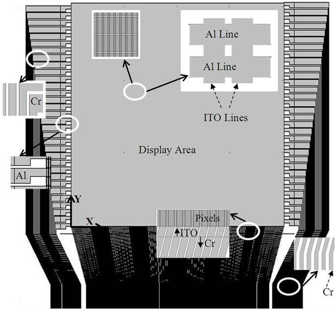
Figure 1. OLED display panel.
μm wide and each line is separated by 25 μm. Then these lines follow a slanted path, narrowing down to 45 μm width and 90 μm pitch corresponding to the dimension of the driver flex to which the display is bonded. Similarly, the 288 ITO columns, approximately 60 μm wide in the active area are narrowed down to 30 μm and 60 μm pitches outside (below) the display.
In the active area of this display are 288 × 64 OLED pixels. From the point of view of thermal analysis, the pixels are the heat sources; in this small display, heat generated in metal lines is insignificant. There are several possibilities for transporting this heat out in order to prevent the display temperature from rising. Since the display is made on the glass, the heat may transport through the glass, which is often also laminated with a polarizer or an antireflection coating. Similarly the heat may be lost through the cap glass used to encapsulate the active area of the display. However, this encapsulation glass is not in physical contact with the OLED pixel area. Therefore, in this case, the heat must also transport through the air-gap in between the pixel and the encapsulation glass or a conduction pathway may be intentionally included above the cathode. In addition to these two modes, the metal lines being good conductor of heat can transport the heat out of the encapsulated area.
Most significant analysis of thermal transport in a display is by Sturm et al. [6] who assume a large display and thus ignore the lateral transport of heat through the metal lines. In their case, heat is transported through the display glass by radiation and convection. Thus, implicitly, there will be no temperature gradient within the emitting area of the display. In a small display, however, Carditz et al. [2] measure brightness inhomogeneity resulting from spatial temperature inhomogeneity. Therefore, we generalize the approach of Sturm et al. to investigate the fraction of heat transported through the metal lines, which in turn can give spatial distribution to temperatures in a display. The model we implement allows for lateral transport of heat, to more accurately determine the temperatures in small displays; later we also discuss the results which would be applicable to larger OLED light sources.
The sources of heat in a display/lighting source are the OLED elements in which electrical power is dissipated partly as light and partly as heat. These sources are closely packed, separated only by few micrometers in either direction. In a numerical simulation, it is neither practical nor necessary to adopt that many node points. Thus, reasonable approximations are discussed first.
The thermal conductivity, K, density, ρ, and specific heat, Cp, of various materials in the display are enumerated in Table 1. Thermal conductivity, K, of the cathode line made of Al is the maximum. The characteristic length for heat conduction through it, Lc, is approximately 20 mm. Thus, with thermal diffusivity, 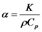 , the heat transit time, ttr
 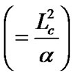 is equal to 13 s. This is the order of time scale in which the heat transport through the longest metal line reaches the steady state. The organic layers, sandwiched between Al cathode and ITO anode, in which the heat is generated are thin, only 200 nm. The corresponding heat transit time is only 0.49 μs. Thus there cannot be a vertical (z-direction) thermal gradient through the organic layer in steady state. Hence, the configuration of two electrodes vertically separated by an organic layer is essentially a 2-dimensional thermal transport problem. Further, the two Al lines are separated by approximately 20 microns, which thermally communicate through ITO lines, rather than the electrical insulator material deployed in the active area to define pixels; this material is even more thermally insulating than the ITO lines. On a 20 μm length scale, the heat transit time in ITO is only 260 μs. Thus, in steady state, there cannot be thermal gradients in –y direction on the length scale that separates two cathode lines. Implication of these facts is that it is possible to construct the metal/organic/metal sandwich in the active area (approximately 20 mm × 15 mm) as a 2-d thermal conduction problem with an effecttive thermal conductivity and a distributed heat source; it is not necessary to solve the problem on the length scales in which the heat sources (pixels) are arranged.
The display region dissipates heat either via metal lines or by convection atop the glass; convective transport from encapsulation glass will be included later. However, the glass layer is thick. A temperature gradient in the glass would then render the problem 3-d. However, Sturm et al. [6] have estimated that the heat transfer coefficient for natural convection is so small that there is no temperature gradient in the glass. This can be specifically shown as follows.
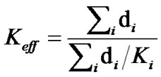
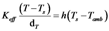
When the OLED is at temperature T, the display surface temperature after glass and polarizer/antireflection coating composite in the z-direction is Ts. Effective thermal conductivity of a composite with conductivity of its components Ki and thickness di is given by
 (1)
(1)
The thermal conductivity of a polarizer or anti-reflection coating is not known. But, a typical 0.2 mm thick organic polarizer consists of layers of polyethylene terephthalate (Ki = 0.54 W/mK [19]), tantalum carbide (22.1 W/mK [20]), polyvinyl alcohol (0.34 W/mK [21]) and an acryl compound (0.49 W/mK [22]) with tantalum carbide layer repeated twice. The thermal conductivity of such polarizer is estimated as 0.7 W/mK according to Equation (1). Similarly, we have estimated thermal conductivity of 180 nm thick antireflection coating consisting of several inorganic layers; that number is also is close to 0.7 W/mK. Thus, for a 1 mm thick glass and 0.2 mm thick polarizer combine, as shown in Figure 2, the effective thermal conductivity (Keff) is 0.88 W/mK. Therefore, at the interface of display glass (with polarizer) and air,
 (2)
(2)
where ambient temperature, Tamb, is 298K, dT = 1.2 mm and h is effective heat transfer coefficient that includes convection and radiation. The heat transfer coefficient (with radiation and convection both) is small, approximately 1 - 10 W/m2K [6]. Further, Ts-298 is also on order of 10 K. Thus, based on Equation (2), T-Ts will be insignificantly small, implying the surface of the display can be regarded at the same temperature as the OLED or that the thermal gradient in z-direction can be neglected.
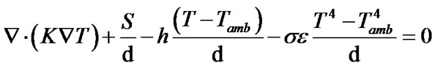
In this case, the heat conduction can be treated only in two dimensions. Accordingly,
 (3)
(3)
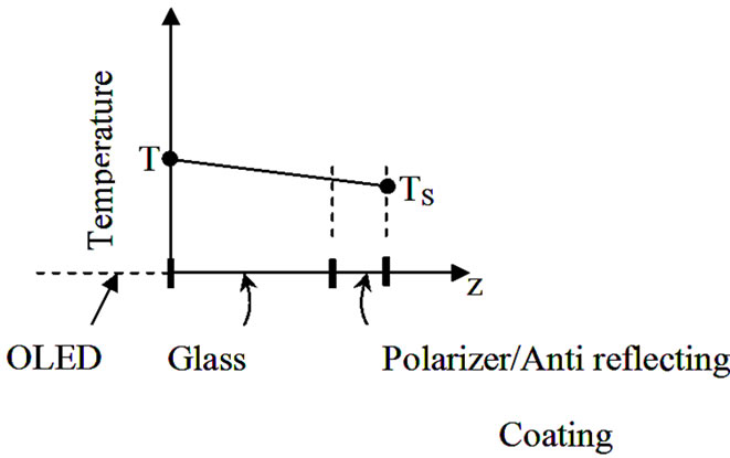
Figure 2. Temperature gradient in an OLED glass with polarizer or anti reflecting coating.
is valid in the entire domain in Figure 1, the display area and the metal lines. In Equation (3), K is either an effecttive thermal conductivity in the active region of the display or that of metal lines, S is a 2-d heat source, in W/m2, due to I2R losses in the OLED. The display dissipates heat from the surface and accordingly convective and radiative losses are included in Equation (3), with σ as StefanBoltzmann constant and e as emissivity of the surface, which for glass is 0.5. The quantity d is the local thickness of material through which the heat is conducted. Therefore, quantities K, T, S, h and d are all position (x, y) dependent and K could also be anisotropic. Finally, since all materials layers are thin, on order of 100 nm, most heat is lost from the surface, of the display or the metal lines. Accordingly, the boundaries within which Equation (3) is valid are considered insulating.
3. Results and Discussion
First we estimate the thermal conductivities, the heat generated in OLEDs and the heat transfer coefficient and then calculate the temperature profiles in the device.
3.1. Thermal Conductivity in the Display Area
There is significant anisotropy in heat conduction in the display area. In x-direction the heat is conducted by Al lines, which are highly conducting, compared to ITO lines. The ITO lines conduct heat in y-direction. Though the display domain is approximated as a homogenous medium with respect to materials, the effect of asymmetric heat flow is accounted for by anisotropy in thermal conductivity in the display domain. Based on the area fraction of the Al or ITO lines, therefore, the thermal conductivity in xdirection is taken as 86.1 W/mK and that in y-direction as 3.3 W/mK. This small change from the values listed in Table 1, however, are insignificant in temperature calculations.
Outside the active display area, the conductivities are of the relevant metal lines according to Table 1.

Table 1. Materials parameters and heat transit time scale.
3.2. Estimate of Heat Generation
Maximum heat is generated in a display when all red (R), blue (B) and green (G) pixels are driven to their highest gray scale, that is, for a white screen. To estimate the heat generation, we use the display we have fabricated as the basis. In order to maintain a white screen, the proportions of luminance (L) for color mixing is as LR = 1.015LB and LG = 2.192LB and with the total (white) luminance of the display L= LR + LB + LG. In a display that has 6144 OLEDs of all three colors each, for various white luminance and corresponding R, G, B OLED luminance, we provide measured current through individual OLED and the corresponding voltage across it in Table 2. For example, a 250 cd/m2 white display would require red OLED of brightness 64.3 cd/m2 in which current sourced is 0.105 mA at 3 V. Similarly, the blue and green pixels should have brightness of 58.2 cd/m2 and 127.5 cd/m2 with corresponding (I, V) as (0.128 mA, 4.1 V) and (0.049 μA and 4.2 V), respectively. Thus, for 6144 R, G and B OLEDs each, total electrical power consumed by the display panel is 6.4 mW. Similar calculations are provided in Table 2 for various brightness values of displays (or equivalent lighting sources) considered in the temperature calculations.
The electrical power that is dissipated is converted to light and heat. Unless specialized techniques are used for light out-coupling, maximum electrical to optical conversion efficiency is 15% - 20%, when efficient phosphoresent materials are used and voltages are low, close to the magnitude of photon energy in eV. In small displays, however, fluorescent materials are common; in those cases, the conversion efficiency may drop between 1% - 5%. In short, most of electrical power is dissipated as heat. In our calculations, as a conservative estimate, we have taken 99% of total electrical power, unless specified differently, being extracted from display as heat. Thus, at brightness of 250 cd/m2, the active area of display being 20.148 × 15.232 mm, the heat source in the active region is S(x, y) = 20.71 W/m2; similar calculations are at other brightness values.
Outside the active region are only metal lines, highly conducting. As part of design principle of a display, we ensure that little power is dissipated in the metal lines. Accordingly, the heat source in metal lines is neglected. Metal thicknesses of Al and ITO, through which heat is conducted laterally in the active area of display, are both 150 nm. The Cr lines are 300 nm. The thickness, d, in Equation (3) is taken accordingly.
3.3. Heat Transfer Coefficient
An extensive discussion on possible convective rates applicable to OLED device is provided by Sturm et al. [6]. For natural convection we follow the same correlations for cases of display held horizontal with face up or held vertical, which are the two most likely situations for a display. It is also possible that the device is held horizontal with face down, as in a lighting fixture. In this case, the heat transfer coefficient is approximately half in value than when it is facing up. Therefore, in Table 3, we report heat transfer coefficients for device held vertical or horizontal with face up. For device held horizontal with face up, Nu = 0.96Ra1/6 and for a vertical device,  , where Nu and Pr are Nusselt and Prandtl numbers and calculations are for Rayleigh number (Ra) as 100 - 200.
But, the display devices are often subjected to conditions of mild forced convection. Therefore, we use correlations that are based on air speed under calm air, light air and light breeze specified in Table 3. For these conditions, 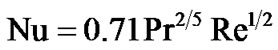 [23] when device is held horizontal facing up and
 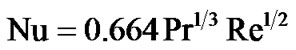 [24] when device is held vertical; Re is the Reynolds number.
Taking in account the values of heat transfer coefficient estimated in Table 3, we could relate the temperature profiles in an OLED device to various conditions in which it is situated by considering h values between 5 - 25 W/m2K.
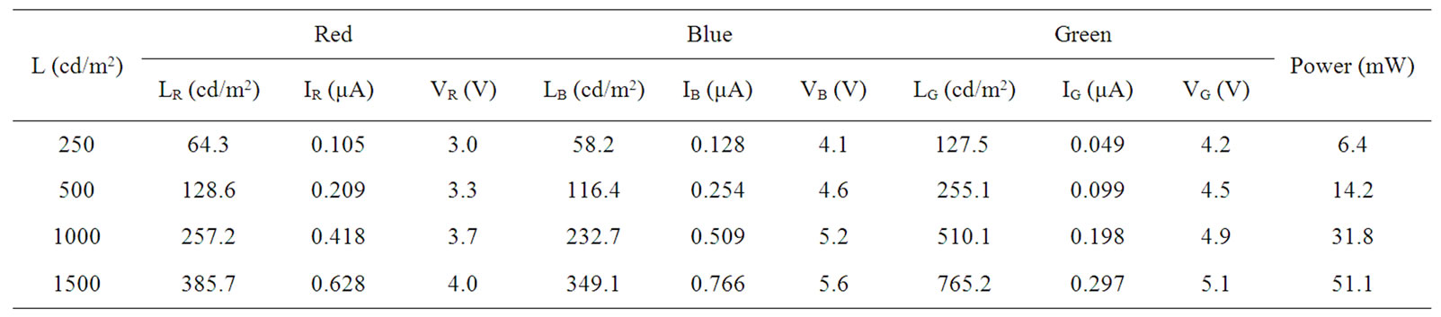
Table 2. Current, voltage, power required for different luminance.
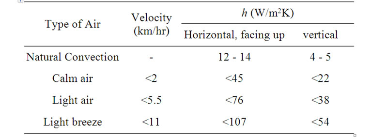
Table 3. Heat transfer coefficient under natural and forced convection.
3.4. Temperature in an OLED Device
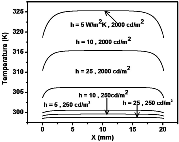
The device is thought to lose heat from the one glass plate and along the metal lines under horizontal or vertical orienttations and natural convection or mildly forced convection. In these conditions, the heat transfer coefficients vary between 5 - 25 W/m2K. Further, a display would typically have brightness of 250 cd/m2 whereas a lighting source may be 2000 cd/m2 bright. For these conditions, in Figure 3, we depict the temperature profiles along the –x and –y directions in the middle of the active area.
In a display operated at 250 cd/m2, the temperature rise is small, approximately 2 K. Therefore, the heat transfer coefficient had little effect on the temperature profile. However, at high brightness, this temperature increase can be as high as 27 K. The temperature increase can be mitigated when the display operates in mildly forced convection, such as air flow in a room, but still the temperature increase is approximately 10 K; consequence of this temperature increase is discussed subsequently. But, clearly, as illustrated in Figure 4, increasing luminance forces higher rise in temperature of device, as expected; this rise is definitely severe under conditions of natural convection.
Further, the impact of including heat extraction along the metal lines can be seen through gradient in temperature near the edges of the display area, due to the cathode lines in Figure 3(a) and anode lines in Figure 3(b). For the display size considered here, the central 60% of the emitting area is at uniform temperature, but the remaining area suffers from a temperature difference of 5˚C - 15˚C, which is sufficient for causing inhomogeneities which were discussed earlier.
The life-time of OLED decreases exponentially with increasing temperature according to . Therefore, percent change in life-time with change in temperature is given by
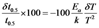 (4)
(4)
which for a 10 K temperature increase above 300 K is 129Ea (Ea in eV). The activation energy is mechanism
 (a)
(a)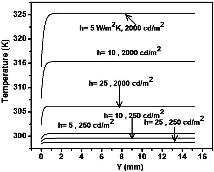 (b)
(b)
Figure 3. Temperature profile in a display operated at two brightness under a range of cooling conditions (a) in center of display along –x direction, that is along cathode lines; (b) in center of display along –y direction, that is along ITO lines.
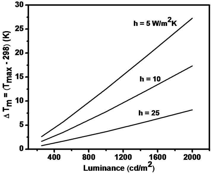
Figure 4. Maximum rise in temperature in a display operated at various brightness levels.
dependent, but typically between 0.1 - 1 eV. For example, in a device based on Alq3 on a steel substrate, this activation energy is reported to be 0.39 eV[8]. In another work in which OLEDs have a N,N’-di(naphthalene-1-yl)- N,N’-diphenyl-benzidine (NPB)/Alq3 interface, the activation energy was determined to be 0.27 eV and related to difference in ionization potential of the two materials [25]. Thus, for activation energy on this order, for example 0.5 eV, the percent decrease in life-time with a 10 K increase in temperature would be 65%.
Even in the earlier devices, the life-time could be seen to decrease by 20% for an increase in temperature by 30 K [26]. But, improved encapsulation method in modern devices has nearly eliminated the reliability issues related to moisture permeation. The life-time had thus increased by one to two orders of magnitude. This life time limited by intrinsic mechanisms of degradation is the one that exhibits exponential dependence on temperature. In other words, the modern devices are lot more susceptible to degradation due to temperature increase.
Apart from luminance homogeneity in a large OLED [2], the light output is also impacted by increasing temperature. For example, Kollar et al. [3] measured optical power output per ampere of current through an OLED to decrease by 1.6 mW/A for a 10K rise in temperature. Similarly, luminous flux decreased by 5% - 10% for 10K increase in temperature in an OLED driven at constant current [4]. This change was accompanied by perceptible change in color coordinates. Clearly, then temperature aberration in an OLED device during operation would have to be managed within a degree centigrade or so above it maximum temperature rating.
3.4.1. Role of Metal Lines in Heat Extraction from the Display
A display which is operated at 250 cd/m2, as depicted in Figure 3, exhibits little temperature variation along either direction. This indicates insignificant contribution of metal lines in extracting heat. But, for example, if a device equivalent in size is used as a unit in making a larger lighting panel and operated at 2000 cd/m2, the temperature variation shown in Figure 3 is significant. Among the three modes by which the device loses heat, indeed convective and radiative loses from the device surface are most important, as indicated in Table 4. However, non-trivial amount of heat is also extracted through the metal lines. Under convection conditions of 5 W/m2K, this heat loss through the metal lines lead to a temperature inhomogeneity (∆T = maximum-minimum temperature in a display) of 14 K (see Table 4 or Figure 3), which is significant. But, when the device is convectively cooled better, the fraction of heat extracted by metal lines decreases and correspondingly the temperature homogeneity improves.
In this context, through Table 5, we indicate that percentage of cooling achieved through metal lines is nearly independent of optical output of the OLED device, except that when total light/power output is small, the heat loss from metal lines is also small enough to not cause any temperature inhomogeneity. Also, when more convective cooling can be ensured, i.e. h changing from 5 to 25 in Table 5, the metal lines play a still smaller role.
3.4.2. Two Sided Cooling
Especially in lighting sources which operate at higher light output, the design of the OLED panel would be more appropriate if cooling of the panel is achieved from both sides. However, in conventional sealing, there is an air gap of approximately 0.3 mm between the device glass and the cover glass, approximately 0.7 mm thick. Effective thermal conductivity of the glass and air gap combined, according to Equation (1) with data in Table 1, is 0.08 W/mK. Thus following the analysis corresponding to Equation (2), the temperature difference between the OLED and cover glass surface will be about 1 K. In this case also, we neglect the gradients in z-direction and Equation (3) remains valid. However, if indeed there is a thermal resistance due to air gap, it will be useful to coat the cathode side of the OLED with materials such as diamond like carbon, which has high thermal conductivity. In any case, for the purposes here, we analyze temperatures according to Equation (3).

Table 4. Cooling modes in a 2000 cd/m2 bright OLED source.
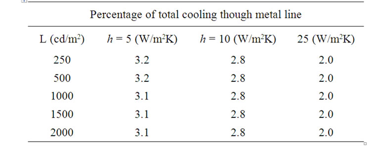
Table 5. Percent heat extracted by metal lines.

Table 6. Display cooled from both sides.
Thus, if the heat transfer coefficient at the device glass is hf and that at the cover glass hb, then total heat transfer coefficient remains h = hf + hb. In Table 6, rise is device temperature is compared with cases when device loses heat only from the front glass, that is hb = 0. Under natural convection, when temperature rise in a device can be as large at 27 K, by cooling from both sides, as expected, the temperature lowers significantly. Rise in temperature is now 17 K, but not half of when cooling is only from one side. But, when calm air flow is available, the temperatures were much lower, and they can be cut in half by designing cooling from both sides of the display. However, it is possible that the cover glass side may not be conveniently accessible, leading to a lower hb. Thus for a case with hf = 10, backside cooling still leads to temperature reduction of 5 K.
4. Conclusions
Inefficient conversion of electrical power into light naturally leads to increase in temperature of an OLED display or lighting panel. Increase in temperature on order of 10 K can have significant impact of life-time of the device, brightness homogeneity or color coordinates of emitted light. And indeed the heat generated in OLED panels is sufficient to raise the temperature by that much amount, as the calculations show.
The heat from the panels should be extracted as much as possible. The role of metal lines in a display which are already present can be exploited. In small displays, a fraction of heat extracted from metal lines lowers the temperature by 5 - 14 K near the edges. This can increase the lifetime but the effect is limited to the edge of the display.
But, two sided cooling of the device, especially in a light panel will be feasible and useful. Thus, design of lighting source should include exposing the back surface as well, which can lower the temperature significantly.
Finally, the thermal transport model presented here for displays is more extensive in its approach and hence likely to provide more accurate results.
5. References
[1] H. Aziz and Z. D. Popovic, “Degradation Phenomena in Small-Molecule Organic Light-Emitting Devices,” Chemistry of Materials, Vol. 16, No. 23, 2004, pp. 4522-4532. doi:10.1021/cm040081o
[2] C. Gärditz, A. Winnacker, F. Schindler and R. Paetzold, “Impact of Joule Heating on the Brightness Homogeneity of Organic Light Emitting Devices,” Applied Physics Letter, Vol. 90, No.10, 2007, pp. 103506-103508. doi:10.1063/1.2711708
[3] E. Kollár, I. Zólomy, and A. Poppe, “Electro-Thermal Modeling of Large-Surface OLED,” Symposium on Design, Test, Integration and Packaging of MEMS/ MOEMS (DTIP’2009), Rome, 1-3 April 2009, p. 239.
[4] A. Poppe, L. Pohl, E. Kollar, Z. Kohari, H. Lifaka and C. Tanase, Semiconductor Thermal Measurement and Management Symposium, 25th IEEE SEMI-THERM, 15-19 March 2009, p. 38.
[5] M. H. M. Lu, M. Hack, R. Hewitt, M. S. Weaver and J. J. Brown, “Power Consumption and Temperature Increase in Large Area Active-Matrix OLED Displays,” Journal of display technology, Vol. 4, No. 1, 2008, pp. 47-53. doi:10.1109/JDT.2007.900924
[6] J. C. Sturm, W. Wilson, and M. Iodice, “Thermal Effects and Scaling in Organic Light-Emitting Flat-Panel Displays,” IEEE Journal of Selected Topic in Quantum Electronics, Vol. 4, No. 1, 1998, pp. 75-82. doi:10.1109/2944.669471
[7] X. Zhou, J. He, L. S. Liao, M. Lu, X. M. Ding, X. Y. Hou, X. M. Zhang, X. Q. He and S. T. Lee, “Real-Time Observation of Temperature Rise and Thermal Breakdown Processes in Organic LEDs Using an IR Imaging and Analysis System,” Advanced Materials, Vol. 12, No. 4, 2000, 265-269. doi:10.1002/(SICI)1521-4095(200002)12:4<265::AID-ADMA265>3.0.CO;2-L
[8] S. Chung, J. H. Lee, J. Jeong, J. J. Kim and Y. Hong, “Substrate Thermal Conductivity Effect on Heat Dissipation and Lifetime Improvement of Organic Light-Emitting Diodes,” Applied Physics Letter, Vol. 94, No. 25, 2009, pp. 253302-253305. doi:10.1063/1.3154557
[9] N. Stojanovic, J. Yun, E. B. K. Washington, J. M. Berg, M. W. Holtz and H. Temkin, “Thin-Film Thermal Conductivity Measurement Using Microelectrothermal Test Structures and Finite-Element-Model-Based Data Analysis,” Journal of Microelctromechanical System, Vol. 16, No. 5, 2007, pp. 1269-1275. doi:10.1109/JMEMS.2007.900877
[10] T. E. Hartman, “Density of Thin Evaporated Aluminum Films,” Journal of Vacuum Science and Technology, Vol. 2, No. 5, 1965, pp. 239-242. doi:10.1116/1.1492434
[11] R. L. Greene, C. N. King, R. B. Zubeck and J. J. Hauser, “Specific Heat of Granular Aluminium Films,” Physical Review B, Vol. 4, No. 6, 1972, pp. 3297-3305. doi:10.1103/PhysRevB.6.3297
[12] T. Ashida, A. Miyamura, N. Oka, Y. Sato, T. Yagi, N. Taketoshi, T. Baba and Y. Shigesato, “Thermal Transport Properties of Polycrystalline Tin-Doped Indium Oxide Films,” Journal of Applied Physics, Vol. 105, No. 7, 2009, pp. 073709-073713. doi:10.1063/1.3093684
[13] H. C. Chien, D. J. Yao and C. T. Hsu, “Measurement and Evaluation of the Interfacial Thermal Resistance between a Metal and a Dielectric,” Applied Physics Letter, Vol. 93, No. 23, 2008, pp. 231910-231913. doi:10.1063/1.3039806
[14] G. P. Zhigal’skii and A. S. Fedorov, “Effect of Formation and Geometric Factor on Flicker Noise in Chromium Films,” Izvestiya Vysshikh Uchebnykh Zavedenii Radiofizika, Vol. 28, No. 9, 1985, pp. 1192-1200.
[15] T. Coquil, C. M. Lew, Y. Yan and L. Pilon, “Thermal Conductivity of Pure Silica MEL and MFI Zeolite Thin Films,” Journal of Applied Physics, Vol. 108, No. 4, 2010, pp. 044902-044907. doi:10.1063/1.3462500
[16] J. H. Simmons, “Refractive Index and Density Changes in a Phase-Separated Borosilicate Glass,” Journal of NonCrystalline Solids, Vol. 24, No. 1, 1977, pp. 77-88. doi:10.1016/0022-3093(77)90063-1
[17] W. Schnelle, J. Engelhardt and E. Gmelin, “Specific Heat Capacity of Apiezon N High Vacuum Grease and of Duran Borosilicate Glass,” Cryogenics, Vol. 39, No. 3, 1999, pp. 271-275. doi:10.1016/S0011-2275(99)00035-1
[18] M. W. Shin, H. C. Lee, K. S. Kim, S.H. Lee and J. C. Kim, “Thermal Analysis of Tris (8-Hydroxyquinoline) Aluminium,” Thin Solid Films, Vol. 363, No.1-2, 2000, pp. 244-247. doi:10.1016/S0040-6090(99)01067-6
[19] R. Kato, A. Maesono and R. P. Tye, “Thermal Conductivity Measurement of Submicron-Thick Films Deposited on Substrates by Modified ac Calorimetry (Laser-Heating Angstrom Method),” International Journal of Thermophysics, Vol. 22, No. 2, 2001, pp. 617-629. doi:10.1023/A:1010745603645
[20] W. S. Williams, “The Thermal Conductivity of Metallic Ceramics,” JOM Journal of Minerals, Metals and Material Society, Vol. 50, No. 6, 1998, pp. 62-66. doi:10.1007/s11837-998-0131-y
[21] G. K. Bama, P. I. Devi and K. Ramachandran, “Structural and Thermal Properties of PVDF/PVA Blends,” Journal of Material Science, Vol. 44, No. 5, 2009, pp. 1302-1307. doi:10.1007/s10853-009-3271-8
[22] F. Tian, L. Sun, J. E. S. Venart and R. C. Prasad, “Thermal Conductivity and Thermal Diffusivity of Poly(Acrylic Acid) by Transient Hot Wire Technique Absolute Measurement,” Journal of Thermal Analysis and Calorimetry, Vol. 96, No. 1, 2009, pp. 67-71. doi:10.1007/s10973-008-9840-2
[23] K. Kitamura and A. Mitsuishi, “Fluid Flow and Heat Transfer of mixed Convection over Heated Horizontal Plate Placed in Vertical Downward Flow,” International Journal of Heat and Mass Transfer, Vol. 53, No. 11-12, 2010, pp. 2327-2336. doi:10.1016/j.ijheatmasstransfer.2010.02.010
[24] J. H. Lienhard IV and J. H. Lienhard V, “A Heat Transfer Textbook,” 3rd Edition, Phlogiston Press, Cambridge, p. 307.
[25] H. Aziz, Z. D. Popovic and N. X. Hu, “Organic Light Emitting Devices with Enhanced Operational Stability at Elevated Temperatures,” Applied Physics Letter, Vol. 81, No. 2, 2002, pp. 370-372. doi:10.1063/1.1491002
[26] J. R. Sheats, H. Antoniadis, M. Hueschen, W. Leonard, J. Miller, R. Moon, D. Roitman and A. Stocking, “Organic Electroluminescent Devices,” Science, Vol. 273, No. 5277, 1996, pp. 884-888. doi:10.1126/science.273.5277.884