Advances in Materials Physics and Chemistry
Vol.3 No.4(2013), Article ID:36086,5 pages DOI:10.4236/ampc.2013.34031
Effect of Substrates on the Properties of ZnO Thin Films Grown by Pulsed Laser Deposition
1Thin Films and Interfaces Laboratory, University of Constantine, Constantine, Algeria
2Advanced Technology Development Center (CDTA), Baba-Hassen, Algiers, Algeria
3Center CRNA, 2 Bd Franz Fanon, Algiers, Algeria
4Laboratory of Applied Optics, Ferhat Abbas University, Setif, Algeria
Email: *Adelphm@Gmail.com, Fouadker@yahoo.fr, Haninifaouzi@gmail.com, Sarahmenakh@yahoo.com, a_bouabellou@yahoo.fr, physique99@gmail.com, tkerdja@cdta.dz, Benazoz@yahoo.com, bouafia_med@yahoo.fr, Amaratoufik@yahoo.fr
Copyright © 2013 Adel Taabouche et al. This is an open access article distributed under the Creative Commons Attribution License, which permits unrestricted use, distribution, and reproduction in any medium, provided the original work is properly cited.
Received February 20, 2013; revised March 22, 2013; accepted April 8, 2013
Keywords: ZnO; Thin Films; PLD; Silicon; X-Ray Diffraction; Optical Transmittance; RBS
ABSTRACT
Polycrystalline zinc oxide (ZnO) thin films have been deposited at 450˚C onto glass and silicon substrates by pulsed laser deposition technique (PLD). The used source was a KrF excimer laser (248 nm, 25 ns, 5 Hz, 2 J/cm2). The effects of glass and silicon substrates on structural and optical properties of ZnO films have been investigated. X-ray diffraction patterns showed that ZnO films are polycrystalline with a hexagonal wurtzite—type structure with a strong (103) orientation and have a good crystallinity on monocrystalline Si(100) substrate. The thickness and compositional depth profile were studied by Rutherford Backscattering spectrometry (RBS). The average transmittance of ZnO films deposited on glass substrate in the visible range is 70%.
1. Introduction
In recent years, there is a great interest in production of transparent conducting oxide (TCO) and transparent oxide semi-conductors for the development of photonic devices and transparent conducting electrodes (TCE) for solar cells [1]. Up to now, a number of studies on ZnO films deposited on various substrates including glass, Si, GaN, GaAs and diamond have been conducted [2-5]. The substrate is very important for the growth of thin films in terms of the lattice and thermal mismatching between it and the film because it commonly leads to the development of stress in the deposited film. It is known that the strain affects the conduction bands of Si, Ge, and direct gap III-V semiconductors differently due to the positions of their band edges in the Brillouin zone. Also, the substrate movement can cause the growth strain-induced in the films. Nucleation and binding of growth species may vary due to the movement of substrate. This affects crystalline quality as well as optical and electrical properties of ZnO film. However, most attentions are paid to the influences of deposition conditions on the properties of ZnO films rather than the substrate selection. Compared to that of polycrystalline, epitaxial growth of ZnO relies more on substrate conditions such as the crystal orientation, the morphology, as well as the inherent property. ZnO thin films are promising materials for various applications due to its large direct band gap of 3.3 eV, low power threshold for optical pumping and a large exciton binding energy of 60 meV at room temperature [6]. Doped and undoped ZnO thin films are currently under intense investigation for use in optoelectronic devices and energy conversion [7].
In this work, the effect of glass and silicon substrates on the structural and optical properties of ZnO thin films grown by pulsed laser deposition has been studied.
2. Experimental
Undoped ZnO thin films were grown onto glass and silicon substrates by the conventional Pulsed Laser deposition (PLD) method. The ceramic pellets (diameter 11 mm and thickness 5 mm) of undoped zinc oxide (ZnO) are prepared using conventional cold ceramic pressing technique using ZnO (99.0%) purity powder obtained from FLUKA Company, and then sintered at 500˚C for 3 h. Before deposition, the substrates were chemically cleaned using acetone and ethanol. The chamber was evacuated by a turbo pump to a pressure of 5 × 10⁻³ Pa, while the partial pressure of the O2 was kept at ~1 Pa. ZnO pellets were ablated by a KrF excimer laser (LAMBDA physik, λ = 248 nm, 5 Hz and 25 ns pulse duration) with a fluence of 2 J/cm2. The distance between the substrate and target was kept fixed at 4 cm and the substrate temperature is maintained at ~450˚C. The beam laser was incident on the rotating target at an angle of 45˚ with respect to the target normal. The thickness and compositional depth profile was studied by Rutherford Backscattering Spectrometry (RBS) using a 2 MeV 4He+ ion beam. The backscattered ions were recorded by a surface barrier detector, placed at 165˚ with respect to the beam. The recorded RBS spectra were processed by the RUMP simulation computer program [8].
The crystalline structure of the synthesized ZnO films was characterized by grazing incidence X-ray diffraction (GIXRD) (Bruker-AXS D8 diffractometer) using CuKα radiation (λ = 0.154056 nm) and operated in θ/2θ configuration. Atomic force microscopy (AFM) (Pacific Nanotechnology) operating in contact mode was used for the observation of surface morphology for ZnO films deposited on different substrates in a region of 2.34 × 2.34 μm2 area. The optical properties of the ZnO thin films were characterized by UV-VIS spectrometer Shimadzu (UV-3101 PC) in the wavelength range 300 - 800 nm.
3. Results and Discussion
3.1. Structural Properties
The (θ - 2θ) XRD patterns of ZnO thin films deposited at ~ 450˚C onto different substrates are shown in Figure 1. The peaks in the spectra of ZnO thin films deposited on glass and Si-Poly substrates confirm the hexagonal wurtzite polycrystalline structure which is in good agreement with (JCPDS 36-1451) data with well-oriented (103) texture. However, in the cases of Si(100) and Si(111) substrates one can note a well textured nature of ZnO films, as indicated by only one peak observed at about 63.25˚. Furthermore a small angular shift of the (103) peak is observed with changing substrates.
The crystallinity of ZnO films determined from the full width at half maximum (FWHM) values of (103) diffraction peak confirms a c-axis preferential orientation.
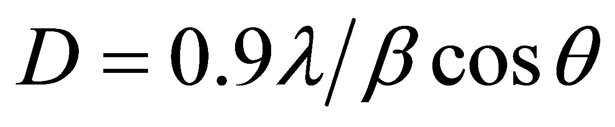
To calculate the average grain size of the samples, the Debye-Scherrer equation is used [9]:
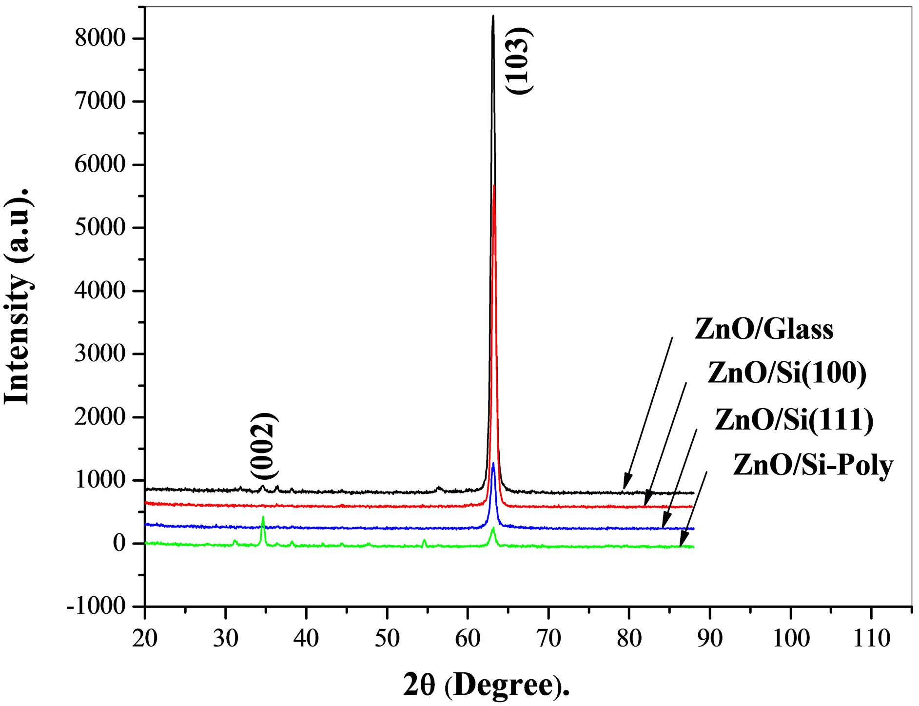
Figure 1. XRD patterns of ZnO films grew on different substrates at 450˚C.
 (1)
(1)
where λ is the X-ray wavelength used, θ is half the angle between the incident and scattered X-ray and β is the FWHM. The values of grain sizes given in Table 1 are found to be in the range from 11 to 17 nm. It is observed that the smallest one corresponds to the ZnO thin films deposited on Si(100) substrate.
It is well known that the (002) orientation of ZnO Wurtzite structure is generally observed, suggesting that the surface free energy of (002) plane is the lowest in ZnO films [10,11]. Indeed, (103) orientation can be formed due to the presence of the residual stress in the film that depends on experimental conditions and substrate nature [12]. In the present work it is clearly seen that ZnO films with (103) orientations are deposited by PLD as shown in Figure 1.
The (103) texture is formed rather than the expected (002) one in the case of glass substrate is in well agreement with previous results [13]. However, in our case, the growth of ZnO films on silicon substrates with (103) orientation may be due to the relatively low O2 gas pressure used during the film deposition. This fact suggests that the oxygen stoichiometry of the obtained ZnO films on Si substrates strongly affects their texture. A better understanding of this phenomenon needs more investigations in the future.
There are non identified peaks just in the case of (SiPoly) substrates, which may be correspond to impurities.
Table 2 shows the different values of a and c lattice parameters of ZnO thin films deposited on glass and SiPoly compared with theoretical values.
ZnO films grow on glass and Si-Poly shows lower c value compared to the bulk value [JCPDS 36-1451], this mean that these films have a compressive strain [14].
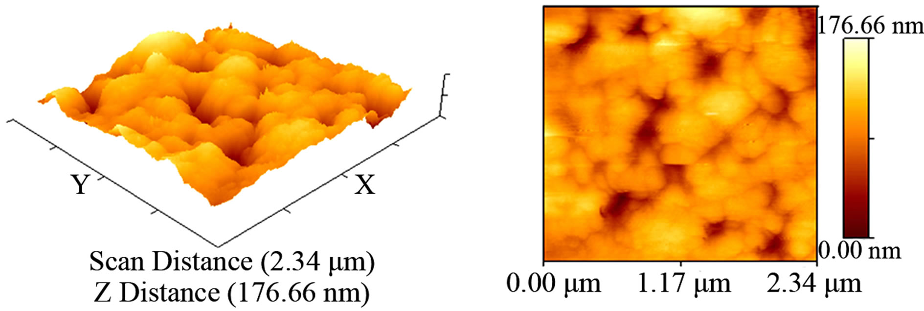
Figure 2 shows AFM topographies of the ZnO thin films deposited on glass and Si-Poly substrates. The
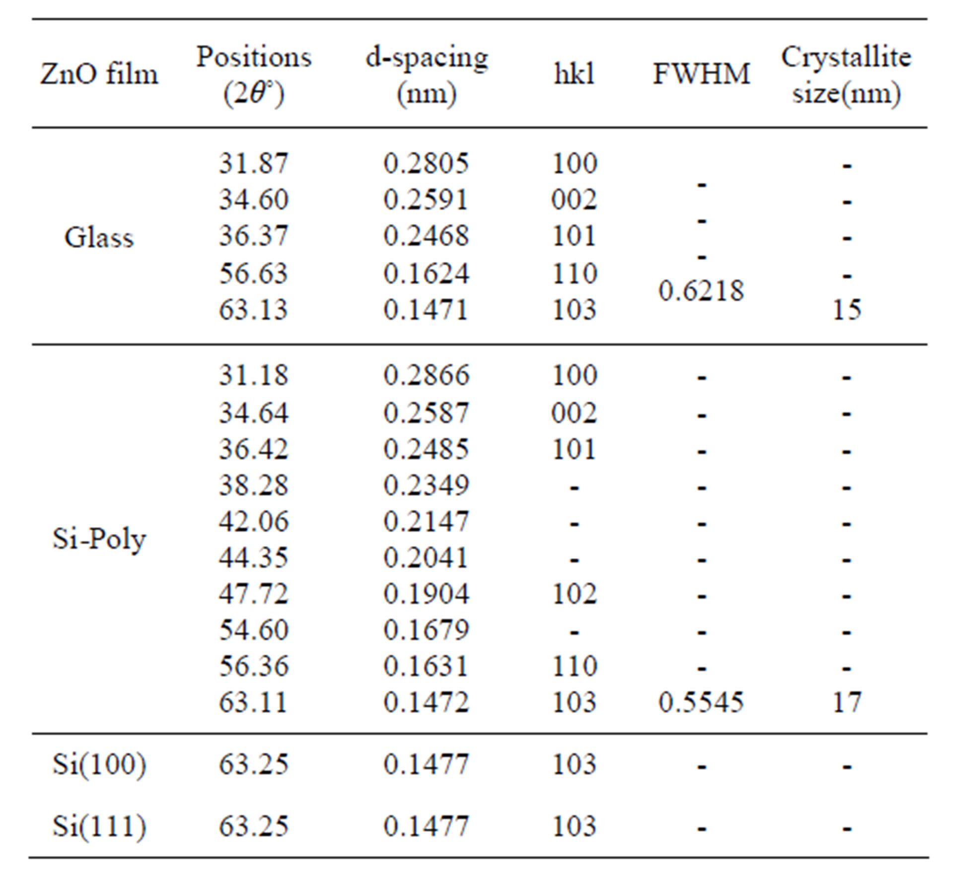
Table 1. Different structural parameters of ZnO thin films deposited on glass and silicon substrates.
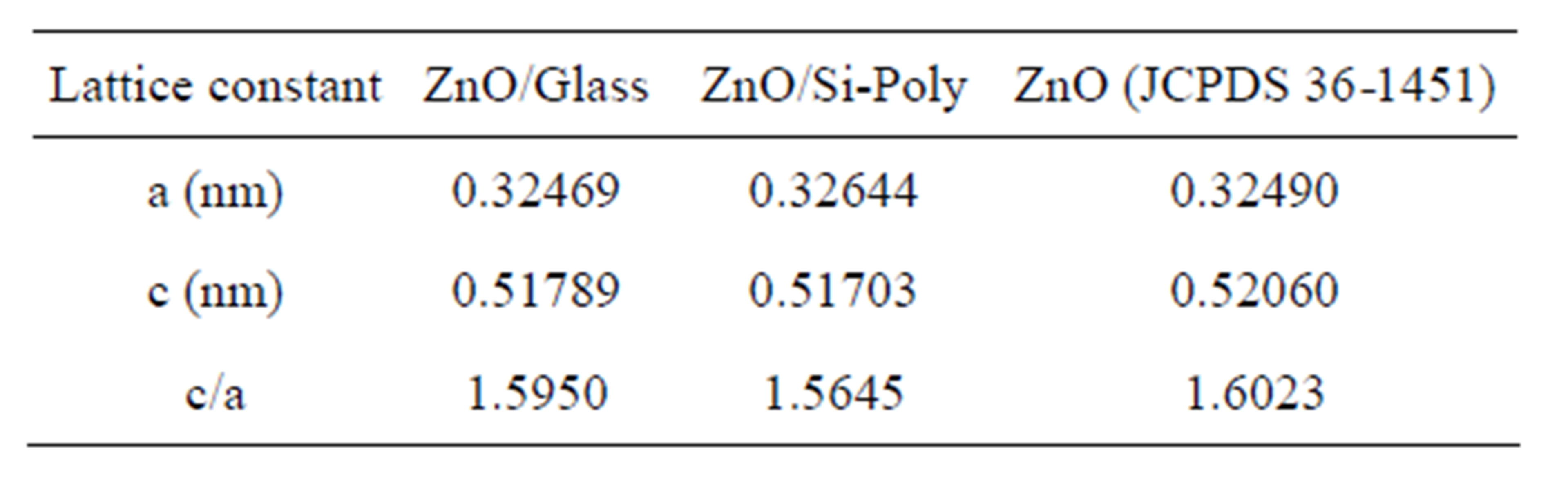
Table 2. Lattice parameters of ZnO thin films deposited on glass and Si-Poly.
 (a)
(a)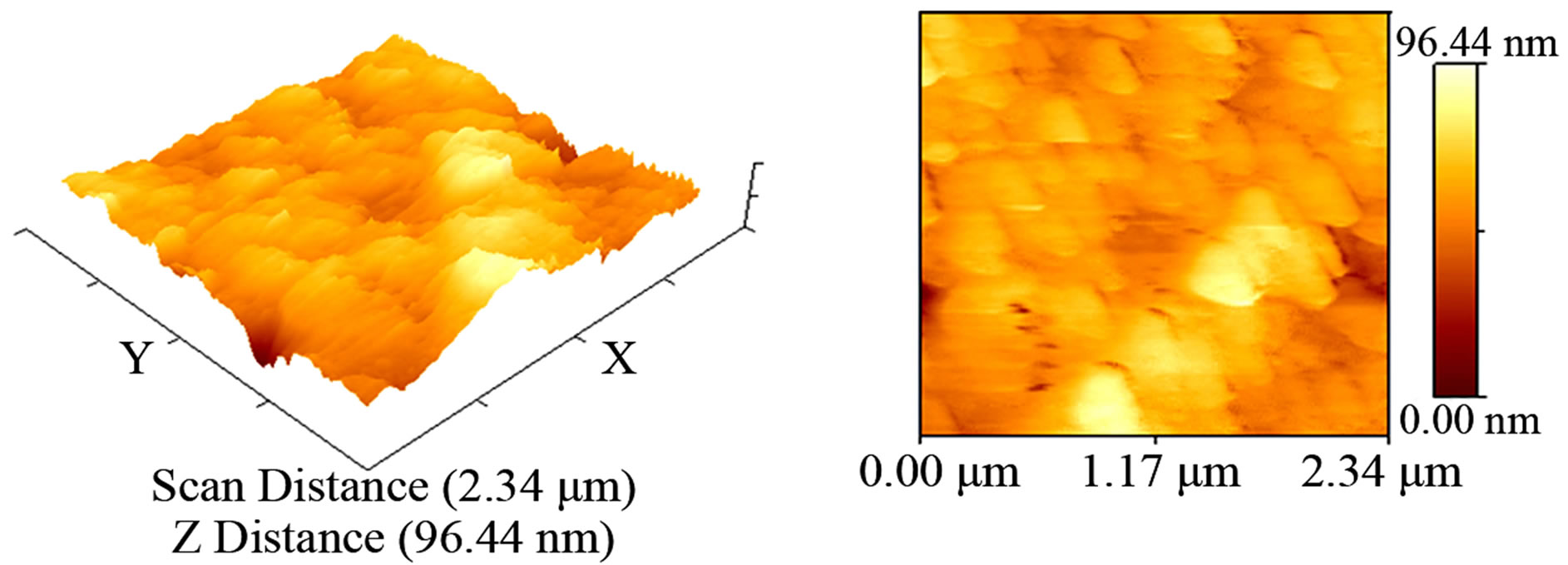 (b)
(b)
Figure 2. AFM images of ZnO thin films deposited on glass (a) and Si-Poly (b) substrates.
mean roughness (Ra) of the surfaces is calculated for a 5.51 μm2 scan area. It is found that the mean roughness significantly decreases from 16 to 7 nm of ZnO films deposited onto glass and Si-Poly substrates respectively. It is known that the increase in surface roughness may cause deterioration of the electrical and optical properties [15]. However, these differences in mean roughness have a significant influence on optical properties of the films considered in this study. These results, together with the XRD analysis, clearly indicate that the crystallinity is influenced by the nature of substrates. This is in good agreement with other results [16].
3.2. RBS Analysis
RBS measurement was used to determine the composition and distribution of the Zn and O elements in the ZnO layers. Figure 3 shows the experimental and simulated RBS spectra of ZnO film deposited on Si(100) substrate. The thickness of ZnO layer is about 370 nm. The atomic composition obtained from RBS analysis is fixed at 42.2 at% O, 57.8 at% Zn.
The experimental RBS spectra were simulated by the RUMP software (Figure 3) and some obtained results are summarized in the Table 3.
3.3. Optical Characterization
Figure 4 shows the transmission spectra of ZnO thin film deposited onto glass substrates in the wavelengths range of 300 - 800 nm. All the measurements are realized at room temperature.
As can be seen, the average optical transmittance of the samples in the visible range is amount 70%. In addition, it is important to notice that the films have a suitable thickness (~370 nm), leading to a good optical quality of the produced ZnO materials which is in good agreement with the literature reports [17,18].
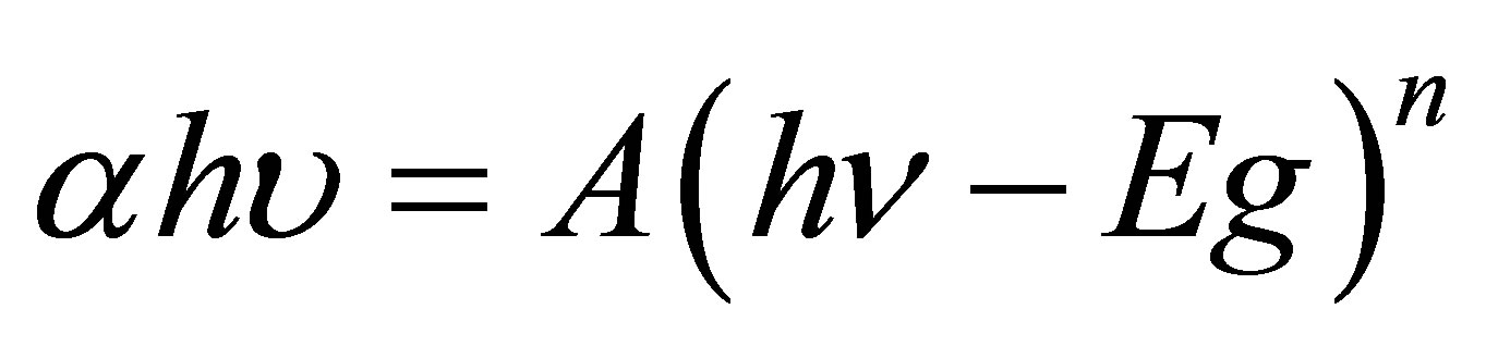
The fundamental absorption edge in most semiconductors follows the exponential law. Above the exponential tail, the absorption coefficient of semiconductors has been observed to obey the relation [19].
 (2)
(2)
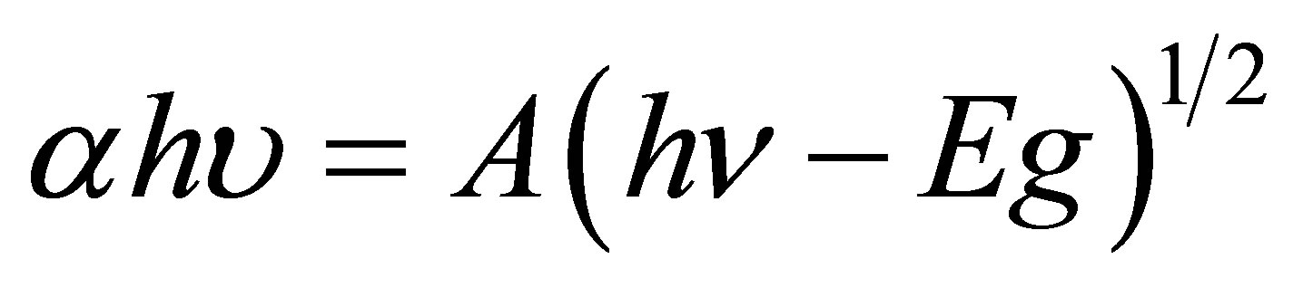
where A is a constant, Eg is the optical band gap energy, and the index can be any value between 1/2 and 3 depending on the nature of the inter-band electronic transition. It has been established that for direct allowed band gap semiconductors, the measured absorption data fits well to Equation (2) for n = 1/2 [13].
 (3)
(3)
The absorption coefficient α could be calculated from the following equation [20]:
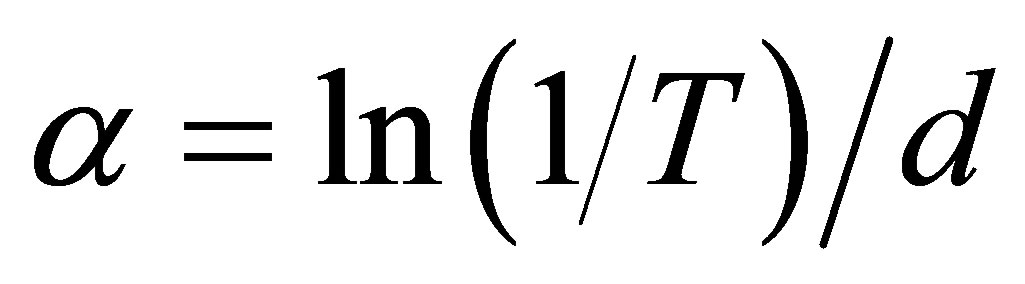 (4)
(4)
where T is the transmittance and d is the thickness of the film. The plot of the graph (αhυ)2 vs hυ (see inset Figure 4) is accomplished using Formula (3). The band gap value of the produced ZnO films, determined by the optical method, is obtained by extrapolating the linear portion of this graph to (αhυ)2 = 0. As can be seen from the
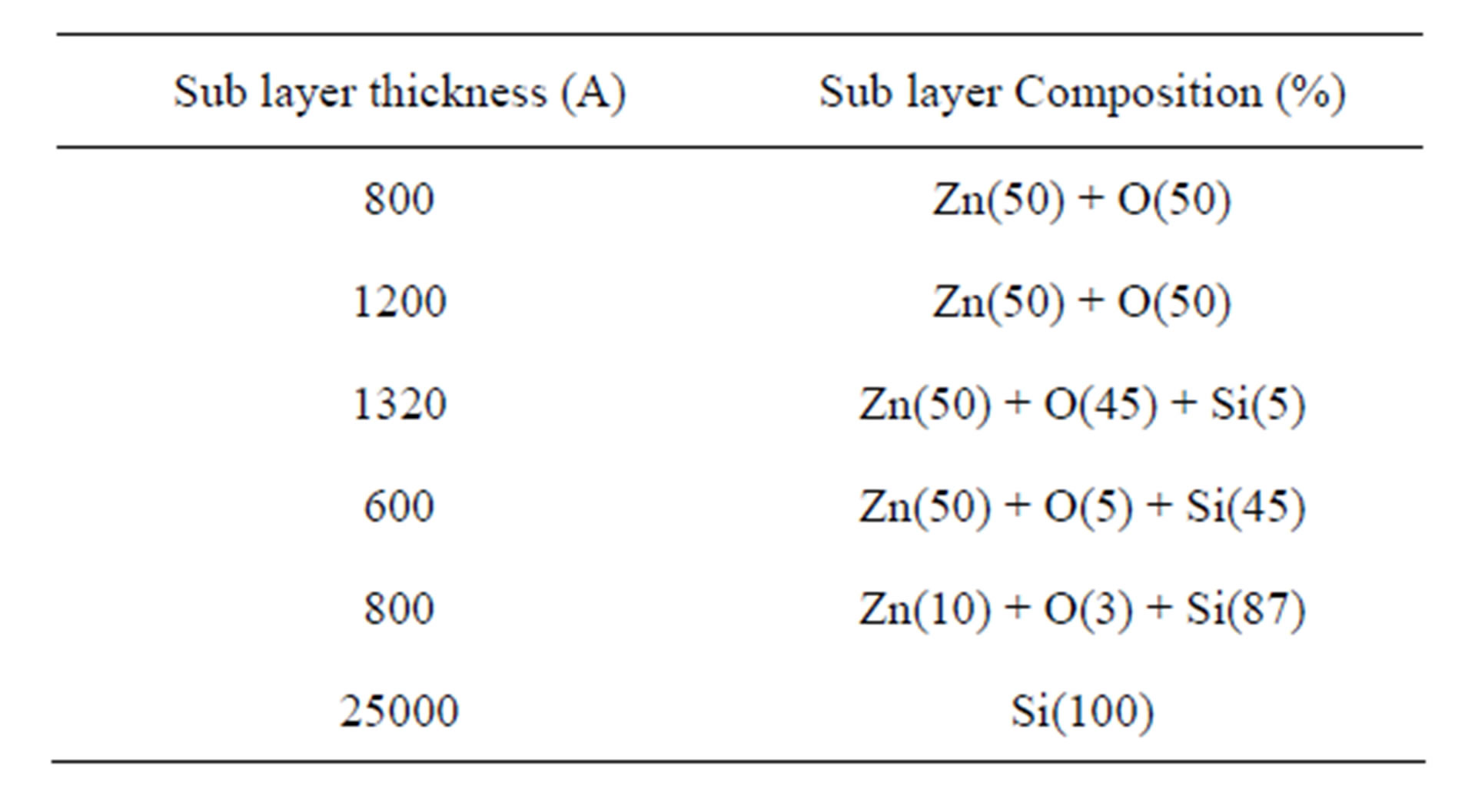
Table 3. Summary of the simulation results.
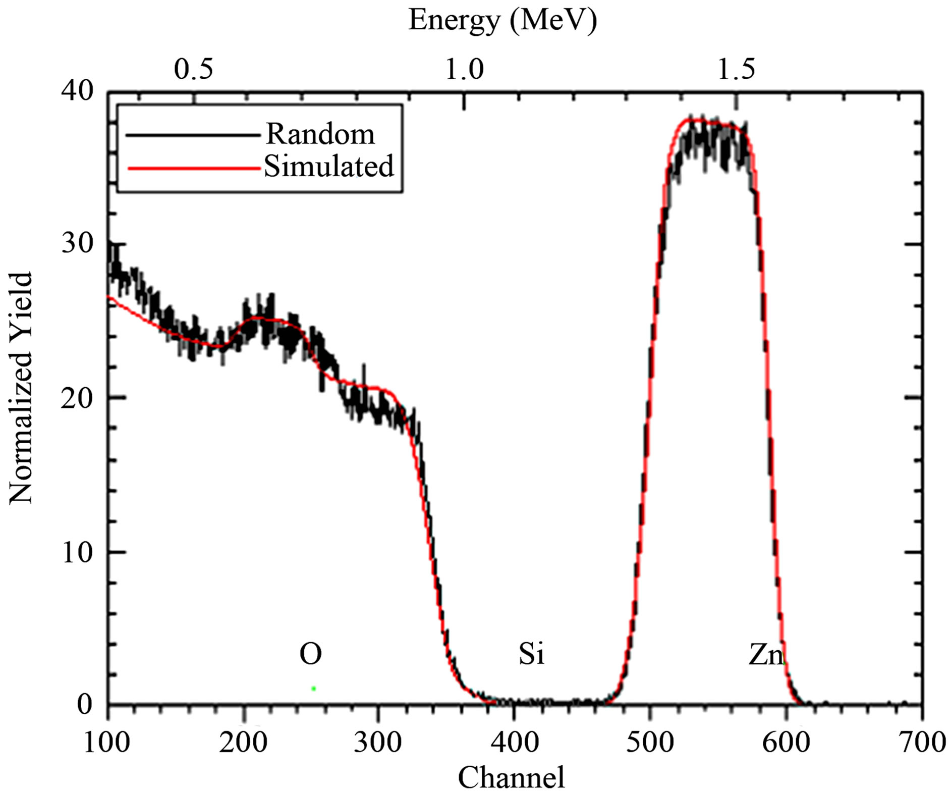
Figure 3. Random and simulated RBS spectra of ZnO films deposited onto Si(100) substrate.
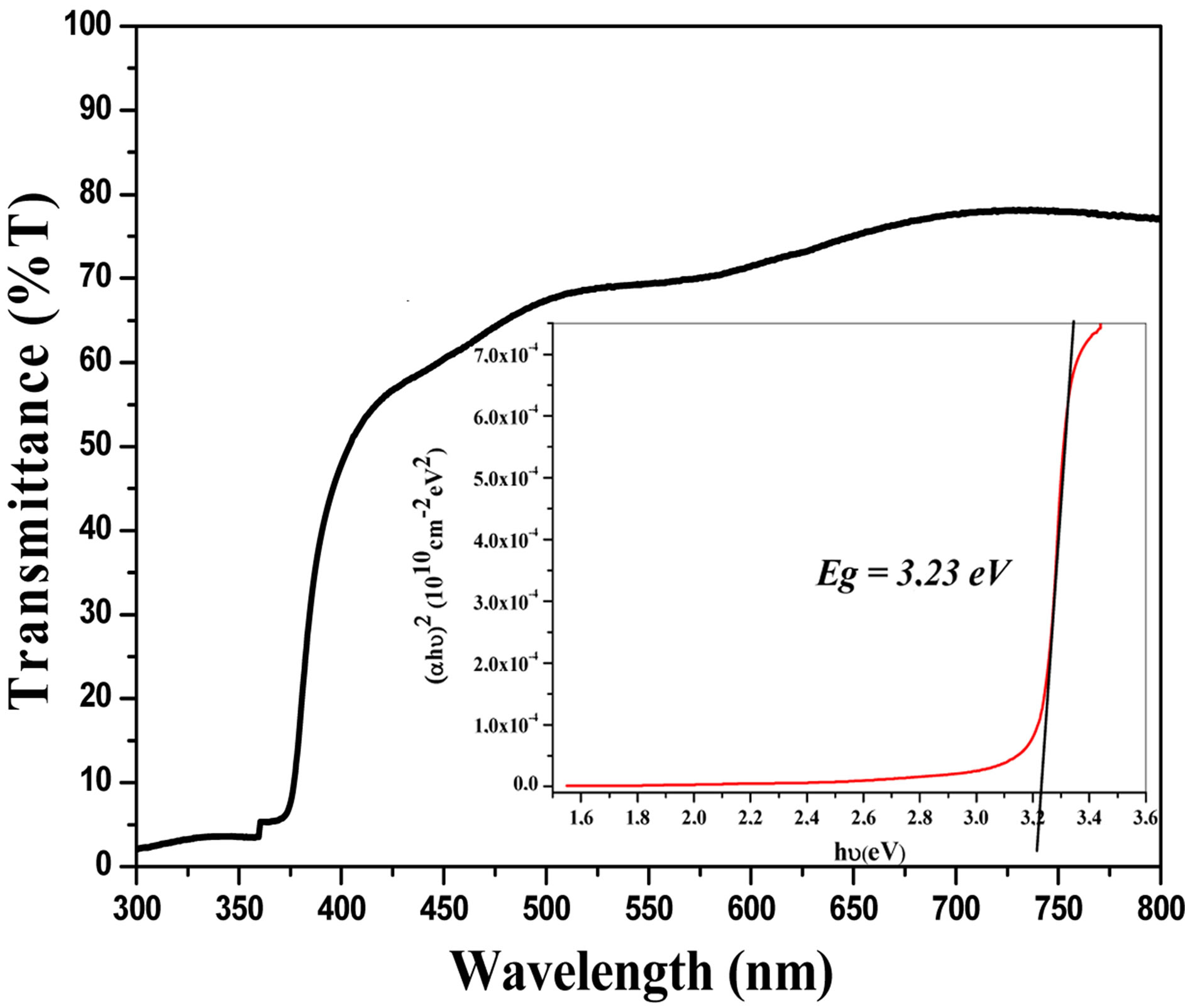
Figure 4. Optical transmittance spectra of ZnO thin films deposited on glass substrate by PLD (The inset shows plot of (αhυ)2 versus hυ.
Figure 4, Eg is equal to 3.23 eV. The glass seems to be the most favorable substrate in the formation of strongly textured ZnO thin films.
4. Conclusion
Properties of ZnO thin films were grown by PLD onto different substrates including glass, Si(100), Si(111) and Si-Poly were investigated. It was observed that the substrate nature has a strong factor influencing the properties of ZnO films. The produced ZnO thin films are polycrystal-line with a texture along the c-axis (103). The values of grain sizes vary from 11 to 17 nm and the mean roughness increases up to 16 nm in the case of the glass substrate. The thickness of ZnO layer is about 370 nm. The atomic composition obtained from RBS analysis is fixed at 42.2 at% O, 57.8 at% Zn. The transmission of the ZnO films is about 70% and the deduced value of their optical band gap is 3.23 eV. There are intrinsic correlations between the structural, optical and morphological properties of the ZnO thin films, which are crucial for future study and application of TCO and solar cells thin films.
REFERENCES
- J. L. Zhao, X. M. Li, J. M. Bian, W. D. Yu and X. D. Gao, “Structural, Optical and Electrical Properties of ZnO Films Grown by Pulsed Laser Deposition (PLD),” Journal of Crystal Growth, Vol. 276, No. 3-4, 2005, pp. 507-512. doi:10.1016/j.jcrysgro.2004.11.407
- K. Shin, K. Prabakar, W.-P. Tai, J.-H. OH and C. Lee, “The Structure and Photoluminescence Properties of Al: ZnO/Porous Silicon,” Journal of the Korean Physical Society, Vol. 45, No. 5, 2004, pp. 1288-1291.
- N.-H. Kim and H.-W. Kim, “Room Temperature Growth of Zinc Oxide Films on Si Substrates by the RF Magnetron Sputtering,” Materials Letters, Vol. 58, No. 6, 2004, pp. 938-943. doi:10.1016/j.matlet.2003.07.040
- S.-K. Hong, T. Hanada, H. Ko, Y. Chen, T. Yao, D. Imai, K. Arak, M. Shinohara, K. Saitoh and M. Terauchi, “Control of Crystal Polarity in a Wurtzite Crystal: ZnO Films Grown by Plasma-Assisted Molecular-Beam Epitaxy on GaN,” Physical Review B, Vol. 65, No. 11, 2002, pp. 115331-115341. doi:10.1103/PhysRevB.65.115331
- M.-Y. Han and J.-H. Jou, “Determination of the Mechanical Properties of r.f.-Magnetron-Sputtered Zinc Oxide Thin Films on Substrates,” Thin Solid Films, Vol. 260, No. 1, 1995, pp. 58-64. doi:10.1016/0040-6090(94)06459-8
- A. Mang, K. Reimann and St. Rübenacke, “Band Gaps, Crystal-Field Splitting, Spin-Orbit Coupling, and Exciton Binding Energies in ZnO under Hydrostatic Pressure,” Solid State Communications, Vol. 94 , No. 4, 1995, pp. 251-254. doi:10.1016/0038-1098(95)00054-2
- D. P. Norton, Y. W. Heo, M. P. Ivill, K. Ip, S. J. Pearton, M. F. Chisholm and T. Steiner, “ZnO: Growth, Doping & Processing,” Materials Today, Vol. 7, No. 6, 2004, pp. 34-40. doi:10.1016/S1369-7021(04)00287-1
- L. R. Doolittle, “Algorithms for the Rapid Simulation of Rutherford Backscattering Spectra,” Physics Research Section B: Beam Interactions with Materials and Atoms, Vol. 9, No. 3, 1985, pp. 344-351. doi:10.1016/0168-583X(85)90762-1
- X. Chen, W. Guan, G. Fang and X. Z. Zhao, “Influence of Substrate Temperature and Post-Treatment on the Properties of ZnO: Al Thin Films Prepared by Pulsed Laser Deposition,” Applied Surface Science, Vol. 252, No. 5, 2005, pp. 1561-1567. doi:10.1016/j.apsusc.2005.02.137
- F. K. Shan, B. C. Shin, S. W. Jang and Y. S. Yu, “Substrate Effects of ZnO Thin Films Prepared by PLD Technique,” Journal of the European Ceramic Society, Vol. 24, No. 6, 2004, pp. 1015-1018. doi:10.1016/S0955-2219(03)00397-2
- K. L. Chopra, S. Major and D. K. Pandya, “Transparent Conductors—A Status Review,” Thin Solid Films, Vol. 102, No. 1, 1983, pp. 1-46. doi:10.1016/0040-6090(83)90256-0
- S. K. Nandi, S. Chakraborty, M. K. Bera and C. K. Maiti, “Structural and Optical Properties of ZnO Films Grown on Silicon and Their Applications in MOS Devices in Conjunction with ZrO2 as a Gate Dielectric,” Bulletin of Materials Science, Vol. 30, No. 3, 2007, pp. 247-254. doi:10.1007/s12034-007-0044-3
- S. Lemlikchia, S. Abdelli-Messaci, S. Lafane, T. Kerdja, A. Guittoum and M. Saad, “Study of Structural and Optical Properties of ZnO Films Grown by Pulsed Laser Deposition,” Applied Surface Science, Vol. 256, No. 18, 2010, pp. 5650-5655. doi:10.1016/j.apsusc.2010.03.026
- R. Vinodkumar, I. Navas, S. R. Chalana, K. G. Gopchandran, V. Ganesan, R. Philip, S. K. Sudheer and V. P. M. Pillai, “Highly Conductive and Transparent Laser Ablated Nanostructured Al: ZnO Thin Films,” Applied Surface Science, Vol. 257, No. 3, 2010, pp. 708-716. doi:10.1016/j.apsusc.2010.07.044
- B. D. Ngom, T. Mpahane, N. Manyala, O. Nemraoui, U. Buttner, J. B. Kana, A. Y. Fasasi, M. Maaza and A. C. Beye, “Structural and Optical Properties of Nano-Structured Tungsten-Doped ZnO Thin Films Grown by Pulsed Laser Deposition,” Applied Surface Science, Vol. 255, No. 7, 2009, pp. 4153-4158. doi:10.1016/j.apsusc.2008.10.122
- C. Li, M. Furuta, T. Matsuda, T. Hiramatsu, H. Furuta and T. Hirao, “Effects of Substrate on the Structural, Electrical and Optical Properties of Al-Doped ZnO Films Prepared by Radio Frequency Magnetron Sputtering,” Thin Solid Films, Vol. 517, No. 11, 2009, pp. 3265-3268. doi:10.1016/j.tsf.2008.11.103
- L. Wang, L. Meng, V. Teixeira, S. Song, Z. Xu and X. Xu, “Structure and Optical Properties of ZnO:V Thin Films with Different Doping Concentrations,” Thin Solid Films, Vol. 517, No. 13, 2009, pp. 3721-3725. doi:10.1016/j.tsf.2008.12.043
- D. Raoufi and T. Raoufi, “The Effect of Heat Treatment on the Physical Properties of Sol-Gel Derived ZnO Thin Films,” Applied Surface Science, Vol. 255, No. 11, 2009, pp. 5812-5817. doi:10.1016/j.apsusc.2009.01.010
- A. Sarkar, S. Ghosh, S. Chandhuri and A. K. Pal, “Studies on Electron Transport Properties and the BursteinMoss Shift in Indium-Doped ZnO Films,” Thin Solid Films, Vol. 204, No. 2, 1991, PP. 255-264. doi:10.1016/0040-6090(91)90067-8
- D. M. Carballeda-Galicia, R. Castanedo-Pérez, O. Jimé- nez-Sandoval, S. Jiménez-Sandoval, G. Tores-Dalgado and C. L. Zũñiga-Romero, “High Transmittance CdO Thin Films Obtained by the Sol-Gel Method,” Thin Solid Films, Vol. 371, No. 1-2, 2000, pp. 105-108. doi:10.1016/S0040-6090(00)00987-1
NOTES
*Corresponding author.