Open Journal of Antennas and Propagation
Vol.05 No.04(2017), Article ID:80970,11 pages
10.4236/ojapr.2017.54013
Design of Wideband PBG Antenna for New Generation Communication Systems through Simulation
Smrity Dwivedi
Indian Institute of Technology (BHU), Varanasi, India
![]()
Copyright © 2017 by author and Scientific Research Publishing Inc.
This work is licensed under the Creative Commons Attribution International License (CC BY 4.0).
http://creativecommons.org/licenses/by/4.0/


Received: November 6, 2017; Accepted: December 8, 2017; Published: December 11, 2017
ABSTRACT
In modern wireless communication system, demand of high bandwidth antennas with low cost are increased. In proposed paper, these requirements have been fully justified by using PBG based wideband antenna. Although, metamaterial is one more option to build this idea, sometimes, negative permittivity or negative permeability or both does not permit to allow easy fabrication and maintaining low cost. An antenna with several periodic rods and organic magnetic materials substrate made it possible to enhance the bandwidth and think off using it for 5G communication systems. Proposed antenna is designed and fabricated for frequency range of 40 GHz - 50 GHz, and 12 × 9 periodic rods with substrate having organic magnetic materials property. Antenna is designed and analyzed using commercial simulation software CST microwave studio (CST STUDIO SUITE 2014) and measured for return loss and VSWR for fabricated design. Obtained results meet the requirement of wider bandwidth of 1.5 - 2 GHz and return loss, −35 dB, and directivity is 61 dBi with efficiency of 61%.
Keywords:
Rectangular MSA, PBG Structure, Teflon, Radiation Pattern, Gain

1. Introduction
Mobile communication and bandwidth requirement for the fast access of multimedia have increased the demand of smart antenna design and development to fit into new generation system. Initially users were interested in third generation cellular systems and less aware of new technologies. After introduction of fourth generation cellular systems, demands are being increased and now research on 5G systems, increases curiosity of users. Although, researchers have been working for few years, on design of new generation systems and have got valuable outputs in an antenna design. But, cost and fabrication of such antennas are high as well as bandwidth enhancement is not fulfilling the requirement of new technologies. From larger size antennas to thinner size antennas have been developed as per need and users’ requirement. As simple microstrip patch antennas played an important role in communication through wireless connections [1] [2] , complicated one is also bringing the fifth generation advance technology and more users in a limited channel. Many researchers have already proved the effect of parameter variations to measure the effective values of desired quantities. Moreover, antenna miniaturization techniques are also being used to develop and install to improve the radiation properties.
Microwave photonic band gap (PBG) structures have their own specific properties that are different from optics. First, the higher wavelength means bigger absolute tolerances than in optics. Secondly, capacitance and inductance are specific properties, not directly seen in optics, because which can vary shape characteristics impedance and make influence on the formation of band gaps. 3-D PBG is complicated for simulation, realization and investigation, due to dependency over the angle of incident and on polarization (may be cross polarization). Quasi 3-D and 2-D structure are more successful and is being improvised to enhance and isolate the antennas characteristics and photonic crystal based waveguide. PBG implantation in antenna design improves the directivity and total gain [3] [4] [5] . It incorporates mainly: suppression of higher harmonics, suppression of the current surface waves, which is the biggest challenge for antenna designers. As surface waves radiate from the roughness of the substrate edges and can cause a problems to the radiation pattern.
The PBG structure is implanted over a dielectric substrate periodically for microwave and millimeter device applications. Electromagnetic wave flows through the stop band with frequency depending upon the pattern geometry and its dimension. If antenna operating frequency falls within this stop band, it is attenuated while propagating through it. Radiation of surface can easily be removed. Figure 1 shows different transmission lines on PBG material.
The basic problem with microstrip patch is narrow bandwidth, which can be improved by increasing the substrate thickness, causes low gain and low efficiency. PBG is most promising solution to increase the frequency and by using it, can be removed many problems like oscillator type active antenna using MESFET or Gunn diode, which has spurious radiation near its operating frequency and low gain of MSA. Frequency selective surfaces (FSS) are a low cost printed electromagnetic material, used to control the surface currents and this is usually implanted by two dimensional arrays of metallic patterns and this is achieved by using multiple layers of FSS as part of the substrate, where they are treated as screens and each screen is resonant at a given frequency and is placed at a distance of λ/4 [6] [7] .
New era of antennas deal with printed antenna suitable for wireless communication equipments and mobile phones, as demand increases complexity
 (a)
(a)
 (b)
(b)
 (c)
(c)
 (d)
(d)
Figure 1. Microstrip line on a usable substrate (a); microstrip line on a PBG substrate (b); microstrip line on a PBG substrate with a defect (c) and (d) [3] .
increases, in terms of feature likes compactness, wideband or multiband operation, high gain, diversity reception, uniform radiation pattern, reduced radiation hazards etc. Radiation hazard is an important issue from the point of view of user’s health. PBG concept has been developed and successfully is being applied for millimeter frequency by rejecting all undesired frequency and intensifies the resonant frequency to enhance the limit of bandwidth. This paper will provide very effective bandwidth with lesser cost at same time.
2. Analysis of MSA with PBG Structure
To design of planar microstrip antenna, the very first important parameter is design frequency, which probably has taken in millimeter frequency range, which supports fifth generations’ technologies and that is the resonant frequency of particular antenna. In case of microstrip antenna, three layers are designed, to use it for wide band application. Ground, substrate and patch, form microwave microstrip antenna, in which patch and ground planes act as conductors, and forming the cavity, whereas middle layer substrate provide supports to these two layers, as organic material has been taken as substrate material.
During the analysis, PBG shows the filter characteristics with stop bands and pass bands, through which electromagnetic waves travel. In PBG, stop band characteristics are more preferable for propagation of waves, which can be fully analyzed by getting its dispersion diagram for rectangular PBG microstrip antenna, gives the frequency spectrum at 46.5 GHz to initiate the required mode and neglects the higher harmonics. Mode propagating is TM01 with low losses and high interaction impedance as drawn in Figure 2, reveals the stop band characteristics for designed structure and justify the importance of PBG material. Blue line represents the stop band characteristics where required mode propagates with their normalized resonant frequencies [4] [8] [9] .
Figure 3, reflects the behavior of dielectric (Teflon) with its refractive index after taking PBG structure with gap size , which represents resonant frequencies. Gap size is the periodicity of rods, the main effective part of PBG. By increasing the gap size, effect of refractive index increases, which affect the
antenna performances in terms of gain and directivity by producing dielectric loss and compactness, is decreased [6] [10] .
For simple MSA, the resonant frequency depends on the patch size, cavity dimension, and the filling dielectric constant, given as,
, (1)
where . kmn = wave number at m, n mode, c is the velocity of light, εr is the dielectric constant of substrate, and
, (2)
![]()
Figure 2. Dispersion diagram for PBG structure for required radius of rod 1.5 mm with periodicity of 5 mm.
![]()
Figure 3. Dielectric constant behaviour with normalized periodicity.
As the designed structure behaves as a resonator, so its length, width for non radiating rectangular patch edge at a certain resonance frequency and dielectric constant can be measured according to Equation (1), which is given as,
(3)
, (4)
where fr = resonant frequency, at which the parameters of MSA are calculated. The radiating edge (L) and patch width (W), are usually chosen such a way that it lies within the range , for efficient and enhance radiation. The ratio W/L = 1.5 gives the good performance according to the side lobe and back lobe appearances in radiation pattern, which essentially need to be removed. In usual practice, the fringing effect causes the effective distance between the radiating edges of the patch to be slightly greater than L. Therefore, the actual value of the resonant frequency is slightly less than fr. Taking into account the effect of fringing field, the effective dielectric constant for TM01 mode is derived using [3] [7] . Using these equations, total length can be obtained as,
, (5)
where, εeff = effective dielectric constant and Δl = line extension which is given as,
(6)
(7)
A combination of parallel plate radiation conductance and capacitance susceptance load the both radiating edges of the patch, which can be measured as,
. (8)
where λ0 is the free-space wavelength and wave number k0 = (2πfr)/c. The input conductance of the patch fed on the edge will be twice the conductance of one of the edge slots, which can be obtained as.
. (9)
Here, the patch is fed by microstrip feeding, which is actually a transmission line, so the impedance will vary from zero in the center to the edge resistance approximately as,
, (10)
Now, arranging rods in MSA to make it PBG follows certain rules, because of periodic structure, in which period of rod, T is half of the guide wavelength of a general microwave strip λg, can be written as,
, (11)
where, , (12)
, (13)
Here, MSA is designed in a conventional fashion and surrounded properly by the PBG lattice structure in organic substrate. The period of PBG with square lattice is T = 6 mm. Several cases of return loss with different cell size a relative to the period T are simulated, and an optimum size of the hole a/T = 2/3 is measured. The mutual coupling among rectangular conformal microstrip antenna elements and interconnection feeding scheme are figured out in the design steps. The distance between two elements of proposed array is 12.5 mm, integrated with groove loaded microstrip feeding with the depth lslot. For the matching of input impedance with the antenna can be calculated [4] ,
, (14)
where, Zc is the characteristic impedance of the microstrip, .
3. Results Analysis and Synthesis
Design of PBG antenna for advanced communication is bound for high frequency to achieved higher band width compared to simple MSA. Experimental measurement of such antenna is passing through complex fabrication, which decides the applicability of antenna. So, the parameter selection is highly likely to depend on frequency. Chosen substrate material also affects the gain and directivity. Some good materials are available, which give very good response but at high frequency ambiguity appears. So, by preferring organic magnetic material substrate enhances the response of antenna at millimeter ranges. Microstrip transmission has been taken here for excitation purpose as well as ease of fabrication. Important step while designing the PBG antenna is periodicities, which gives stop band and pass band characteristics clearly. Because of periodic nature of rod having same periodicity represents slow wave behavior of antenna and supports transverse magnetic modes. Other higher modes are also possible but these have return loss more positive and losses are increased. Analysis has been done PBG based structure for frequency approximately 46.5 GHz and results related to this work are properly analyzed using commercial software CST microwave studio (CST 2014). Parameters have been decided by antenna expressions in section III, and have also been checked for ease of fabrication. PBG based antenna has been taken to check the compatibility with 5G advance cellular system technology. For PBG, rods have been taken, putting at equal periodicity. Parameters are considered according to the resonant frequency given in Table 1.
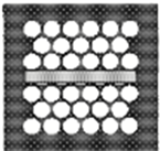
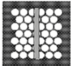
Design structure of proposed antenna PBG microstrip antenna is shown in Figure 4. PBG antenna has periodic rods with same periodicity to form lattice type structure, which has been clearly shown in Figure 3. From the simulated structure, position of patch, ground and several rods are visible. PBG based structure is preferably used for single mode of operation with low loss and highly sensitive to the refractive index. TM01 mode is propagating through the stop bands, which is the dominant mode for the slow wave structure. Fabricated structure of given design is shown in Figure 5. Here, dielectric coating has been done by Teflon magnetic organic material because of its permittivity. Connector

Figure 4. PBG antenna representation with rods, patch and ground.

Table 1. Design specification of PBG Antenna.
is being used to support frequency range 40 GHz to 60 GHz.
The most efficient and affluent parameter is return loss, which is highly likely to affect the antenna design. Return loss indicates the percentage of power reflection in term of S11. For, simple MSA for the same design parameters is less effective even though, value is good. But, introduction of PBG escalates the structure for 5th Generation technology with low losses and higher bandwidth. Return loss is effective, when it is greater in −10 dB in negative side. Figure 6, represents the both experimental and simulation results. Simulation results have been obtained with the help of CST microwave studio commercial software and experimental results is coming using VNA. Plot is showing return loss at two

Figure 5. Fabricated PBG based MSA.

Figure 6. Return loss of PBG antenna, red line Measured experimentally and black line represents Simulation.
frequencies. 42.4 GHz and 46.5 GHz. So, this antenna can work in dual mode, according to frequency requirement. Nature of simulated (black line) and measured (red line) is same, but values of S11 are different. For resonant frequency, 46.5 GHz, measured result is −30 dB and simulated result is −35 dB. This difference is coming because of optimization has not been performed. But, results are very close within a range of 5%.
After getting the return loss, the next important parameter is voltage standing wave ratio in Figure 7, for identifying the matching condition. VSWR, at given frequency 46.5 GHz is 1.3 for measured (red line) and 1.1 for simulated one (black line). Value of VSWR is representing the effectiveness of standing wave pattern with reflection coefficient.
Bandwidth enhancement can be decided from return loss, Figure 7. It is coming approximately 1.5 GHz. Result obtained for bandwidth is showing proper enhancement in wider range and multiple channels can be passed through this range.
Directivity and power pattern are used to check the applicability of designed antenna. Figure 8(a), represents the varying electric field and magnetic field pattern in space coordinate. Main lobe surrounds the major effective area, and few side lobes are appeared because of dielectric and radiation losses. Table associated with plots, is having radiation efficiency and total efficiency as well value of directive gain. Directivity of given antenna is 8.55 dB. Power pattern in Figure 8(b) has electric field values at radiation curve, which is given in table associated with Figure 8(b). Figure 9, is showing azimuthal and elevation planes of radiation pattern and range of electric field from antenna to far field region.
4. Conclusion
Above analysis and obtained results are turned up the interest towards fifth generation and set the basic idea of standardized antenna for advance technologies.

Figure 7. VSWR of PBG antenna, red line measured experimentally and black line represents simulation.
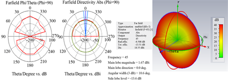
Figure 8. Farfield pattern of PBG antenna in term of directivity (a); effective power pattern (b).

Figure 9. Three dimensional far field pattern from designed structure.
Idea to enhance bandwidth restricts to designer to operate the antenna at allotted frequency range. Thinking off to design antenna at higher frequency usingsome specific structure like PBG, metamaterials, has widen the range of frequency with unlimited use. In above paper, PBG microstrip antenna has been analyzed in terms of return loss, VSWR, gain and bandwidth, which has revealed the utility for advance technologies. Using Teflon as dielectric material is a major change in antenna design. Teflon can be used for terahertz devices too. Efficiency of designed antenna is 61%. Return loss and VSWR at frequency 46.5 GHz are −35 dB and 1.1 respectively. Bandwidth enhancement is 1.5 GHz, which covers many other allotted spectrums and can be used for cognitive radio. Experimental and simulation results are in close agreement.
Cite this paper
Dwivedi, S. (2017) Design of Wideband PBG Antenna for New Generation Communication Systems through Simulation. Open Journal of Antennas and Propagation, 5, 169-179. https://doi.org/10.4236/ojapr.2017.54013
References
- 1. Ziolkowski, R.W. and Erentok, A. (2006) Metamaterial-Based Efficient Electrically Small Antennas. IEEE Transactions on Antennas and Propagation, 54, 2113-2130. https://doi.org/10.1109/TAP.2006.877179
- 2. Dwivedi, S. (2017) Simulation Analysis on Applicability of Meta Material and PBG Based mm-Wave Planar Antenna for Advanced Cellular Technologies. Open Journal of Antennas and Propagation, 5, 23-35. https://doi.org/10.4236/ojapr.2017.51003
- 3. Tarot, A-C., Collardey, S. and Mahdjoubi, K. (2003) Numerical Studies of Metallic PBG Structures. Progress in Electromagnetics Research, PIER 41, 133-157. https://doi.org/10.2528/PIER02010806
- 4. Wang, X., Zhang, M. and Wang, S.-J. (2011) Practicability Analysis and Application of PBG Structures on Cylindrical Conformal Microstrip Antenna and Array. Progress in Electromagnetics Research, 115, 495-507. https://doi.org/10.2528/PIER11031703
- 5. Guha, D. (2015) Microstrip and Printed Antennas. Willey Publication, Hoboken.
- 6. Krauss, J.D. (2001) Antennas For All Applications. 3rd Edition, McGraw-Hill, New York.
- 7. Zavosh, F. and Aberle, J.T. (1996) Improving the Performance of Microstrip Patch Antennas. IEEE Antenna and Propagation Magazine, 38, 712-721. https://doi.org/10.1109/74.537361
- 8. Mailloux, R.J., Mcllvenna, J.F. and Kemweis, N.P. (1981) Microstrip Array Technology. IEEE Transactions on Antennas and Propagation, 29, No.1. https://doi.org/10.1109/TAP.1981.1142525
- 9. Munroe, B., Cook, A., Shapiro, M. and Temkin, R. (2012) High-Gradient Photonic Bandgap (PBG) Structure Breakdown Testing at Ku-Band. Proceeding of IPAC2012, New Orleans, 20 May 2012.
- 10. Yang, F.-R., Coccioli, R. and Qian, Y.X. (2000) Planar PBG Structures: Basic Properties and Applications. IEICE Transactions on Electronics, E83-C, No. 5.