Journal of Surface Engineered Materials and Advanced Technology
Vol.4 No.5(2014), Article
ID:48552,8
pages
DOI:10.4236/jsemat.2014.45028
Dependence of Atomic-Scale Si(110) Surface Roughness on Hydrogen Introduction Temperature after High-Temperature Ar Annealing
Koji Araki1*, Ryuji Takeda1, Haruo Sudo1, Koji Izunome1, Xinwei Zhao2
1Base Technology, Technology, Global Wafers Japan Co., Ltd., Niigata, Japan
2Department of Physics, Tokyo University of Science, Tokyo, Japan
Email: *Koji_Araki@sas-globalwafers.co.jp
Copyright © 2014 by authors and Scientific Research Publishing Inc.
This work is licensed under the Creative Commons Attribution International License (CC BY).
http://creativecommons.org/licenses/by/4.0/


Received 12 June 2014; revised 11 July 2014; accepted 27 July 2014
ABSTRACT
The atomic-scale surface roughness of Si(110) reconstructed via high-temperature Ar annealing is immediately increased by non uniform accidental oxidation during the unloading process (called reflow oxidation) during high-temperature Ar annealing. In particular, for a reconstructed Si(110) surface, characteristic line-shaped oxidation occurs at preferential oxidation sites appearing in pentagonal pairs in the directions of Si[-2]">112] and/or [-11-2]. We previously reported that the roughness increase of reconstructed Si(110) due to reflow oxidation can be restrained by replacing Ar gas with H2 gas at 1000˚C during the cooling to 100˚C after high-temperature Ar annealing. It was speculated that preferential oxidation sites on reconstructed Si(110) were eliminated by H2 gas etching and hydrogen termination of dangling bonds. Thus, it is necessary to investigate the effect of H2 gas etching and hydrogen termination behavior on the reconstructed Si(110) surface structure. In this study, we evaluated in detail the relationship between the temperature at which the H2 gas replaces the Ar in high-temperature Ar annealing and the reconstructed Si(110) surface structure. The maximum height of the roughness on the reconstructed surface was the same as if Ar gas was used when the H2 gas introduction temperature was 200˚C, although the amount of reflow oxidation was decreased to 70% by hydrogen termination. Furthermore, line-shaped oxidation still occurs when H2 gas replaces Ar at this low temperature. Therefore, we conclude that oxidation is caused by slight Si etching at low temperatures, and thus the preferential oxidation sites on the reconstructed structure must be eliminated by hydrogen etching in order to form an atomically smooth Si(110) surface.
Keywords:Si(110), Surface Roughness, Hydrogen Termination, High-Temperature Ar Annealing

1. Introduction
Semiconductor integrated circuits are the most important hardware technology in today’s technologically advanced society. Improvements in the performance of semiconductor integrated circuits have been driven primarily by Si field-effect transistors (a type of metal-oxide-semiconductor field-effect transistor, MOSFET), which are the smallest constituent units of high-performance circuits. To improve the performance of semiconductor integrated circuits, it is essential to enhance the current-driving ability and reduce the power consumption of a transistor. Until now, these requirements have been met mainly by scaling the transistor structure. However, scaling will face limitations in near future [1] [2] , and so it is very important to establish a performance improvement method other than scaling.
Surface scattering at the Si/silicon dioxide (SiO2) interface in MOSFETs can reportedly be decreased by forming an atomically smooth Si surface. Moreover, such a smoothing process can also enhance the carrier mobility of MOSFETs [3] -[5] . In other words, controlling the Si surface structure with a high degree of accuracy can enhance the current-driving ability and reduce the power consumption of a transistor. Thus, control of the atomic surface structure of Si is important for future metal oxide semiconductor (MOS) large scale integration (LSI) technology.
It is well known that a smooth surface on Si wafers can be realized by wet hydrogen fluoride (HF) cleaning at room temperature or by high-temperature annealing [6] -[8] . Wet HF cleaning provides an atomically flat surface on Si(111), but it is difficult to maintain the obtained degree of flatness because the surface structure changes at low temperatures [9] . Furthermore, Si(100), which is used for the commercial manufacture of MOS LSI circuits, is not smoothed by wet HF cleaning at room temperature. In addition, there have been no reports on the surface smoothing of Si(110), which has a higher carrier mobility than Si(100).
In contrast, high-temperature annealing provides atomically smooth surfaces on both Si(100) and Si(110). Furthermore, high-temperature annealing in a furnace is a useful industrial process and can be used to process around 100 wafers in one batch. Kumagai et al. reported that the surface of a Si substrate annealed at 900˚C or above will contain well-developed terraces with monoatomic steps [10] . The width of a terrace formed by high-temperature annealing is dependent on the off-angle of the Si wafer, and it is necessary to maintain a small off-angle to obtain a wide terrace [7] . They also reported that annealing a Si surface in an H2 atmosphere causes etching of the surface, which affects the surface roughness [10] . However, during the thermal process for improving the surface roughness of Si, it is necessary to consider not only the etching of the Si surface by H2 gas but also the effect of accidental oxidation, which results in the growth of thermal oxide films and affects the Si surface roughness. For example, the surface roughness increases with increasing in the oxide layer thickness on the surface of a Si substrate [11] . Generally, the formation of an oxide layer on the surface of a Si substrate is not observed during high-temperature annealing in either an Ar or an H2 atmosphere. However, oxidation might occur during unloading, which is called reflow oxidation [12] . In this process, the atmosphere gas is changed to air at relatively high temperatures. We have found that restricting the reflow oxidation during high-temperature annealing is very important for maintaining the smoothness of a reconstructed surface [12] . We clarified that the surface roughnesses of both Si(100) and Si(110) decreased with decreasing thickness of the reflow oxidation layer. However, high-resolution atomic force microscopy (AFM) revealed that reflow oxidation still caused a variation in the surface roughness.
In particular, characteristic line-shaped oxidation occurs at preferential oxidation sites appearing in pentagonal pairs in the directions of Si[-2]">112] and/or [-11-2] on a reconstructed Si(110) surface. This line-shaped oxidation causes a height fluctuation of approximately two atomic layers (0.24 nm) in AFM measurements, which is an obstacle for decreasing the Si(110) surface roughness.
Thus, we have attempted to find other effective methods for restraining the influence of reflow oxidation. One such method is hydrogen termination (H-termination), i.e., terminating dangling bonds with hydrogen. This method provides a chemically inert surface that was found to restrain the growth of native oxides at room temperature [13] . Thus, we assume that the use of an unloading process with a perfect H-terminated Si surface would be a good method for suppressing reflow oxidation. In addition, replacing the injected Ar gas with H2 gas during the cooling process for high-temperature Ar annealing is another effective method for reducing the effect of reflow oxidation. However, the Si surface structure is also etched when H2 gas is used. Therefore, it is necessary to investigate the effects of H2 gas etching and H-termination on the reconstructed Si(110) surface structures.
We previously reported that the roughness increases of reconstructed Si(110) due to reflow oxidation can be restrained by replacing Ar gas with H2 gas at 1000˚C in the process of cooling the wafer to 100˚C after high-temperature Ar annealing [14] . We speculated that this effect is due to the elimination of the preferential oxidation sites on reconstructed Si(110) by H2 gas etching and H-termination of dangling bonds. To obtain a better understanding of this process, in this study, we evaluated in detail the relationship between temperature at which H2 gas replaces the Ar after the high-temperature Ar annealing and the reconstructed Si(110) surface structure.
2. Experiments
Boron-doped Czochralski-grown Si(110) polished wafers (200 mm in diameter) with off-angles below 0.1˚ were used. Their electric resistivities were 15 Ω∙cm. The sample wafers were heat-treated at 1200˚C for 1 h in an Ar atmosphere by using a commercial vertical furnace. We chose the two temperature ranges, 1000˚C - 100˚C and 200˚C - 100˚C, in which the Ar in the furnace was replaced with H2 during the cooling process to obtain a better understanding of the changes in the surface structure due to the introduction of H2 gas. Under the former condition, which was used in our previous work [14] , no line-shaped oxidation occurred. Nearly the same results are expected for the new 200˚C - 100˚C temperature range; the only difference should be the Si etching effect, which depends on the temperature. Therefore, a better understanding of this process can be gained by comparing the results obtained for these two cases.
H-termination on the Si surfaces was confirmed by Fourier transform infrared attenuated total reflection (FT-IR-ATR) spectroscopy carried out using a Bruker IFS-120HR system. The thickness of the oxide film on the surface was determined by X-ray photoelectron spectroscopy (XPS) carried out using a PHI Quantera SXM XPS spectrometer. The surface structure of the samples was observed using an atomic force microscope (Digital Instruments Nanoscope IIIa) operated in tapping mode. The measurement fields had areas of 3 × 3 and 0.2 × 0.2 μm2. The first measurement area was used to observe the reconstructed surface of an annealed wafer, which generally consists of a step/terrace structure, and the second measurement area was used to observe in detail a single terrace at a time.
3. Results and Discussion
We investigated the effect of changing the injected gas from Ar to H2 during the cooling process on the silicon oxide (SiO) layer formed on the surfaces of Si(110) wafers during high-temperature Ar annealing. The thickness of the oxide layer after the annealing process was measured by FT-IR-ATR and XPS. Figure 1 shows the FT-IR-ATR spectra for Ar-annealed Si(110) wafers in the wave number range of 2000 - 2300 cm−1. Spectra (i) - (iv) were obtained before Ar annealing (w/o Ar annealing), after Ar annealing using Ar gas during the cooling process (Ar-cooled), after Ar annealing using H2 gas during the cooling process from 200˚C (H2-cooled_ 200˚C), and after Ar annealing using H2 gas during the cooling process from 1000˚C (H2-cooled_1000˚C), respectively.
In the spectra for the H2-cooled samples, three significant peaks were observed at 2089, 2013.7, and 2250 cm−1. The strong peaks at 2089 cm−1 and 2103.7 cm−1 were only observed for the samples cooled in H2 atmospheres, and were assumed to originate from Si-H and Si-H2 bonding, respectively [15] [16] . The peak at 2089 cm−1 was strongest for the H2-cooled_200˚C sample, whereas the 2013.7 cm−1 peak was strongest for the H2-cooled_1000˚C sample in our previous work [14] . On the basis of reported examples [15] [16] , the Si-H2 bonding in Si(110) is considered to result from the breaking of dimers and back bonds and the formation of terminal Si-H2 bonds during H2 atmosphere annealing. Thus, we assume that surface was etched by H2 during the cooling process at 1000˚C. On the other hand, Si-H bonds, which produce the 2089 cm−1 peak that is dominant for the H2-cooled_200˚C sample, are known to be the typical H-termination structure of Si(110) [15] [17] . Therefore, it is speculated that the surface of the H2-cooled_200˚C sample was only slightly etched by H2 gas, unlike that of the H2-cooled_1000˚C sample.
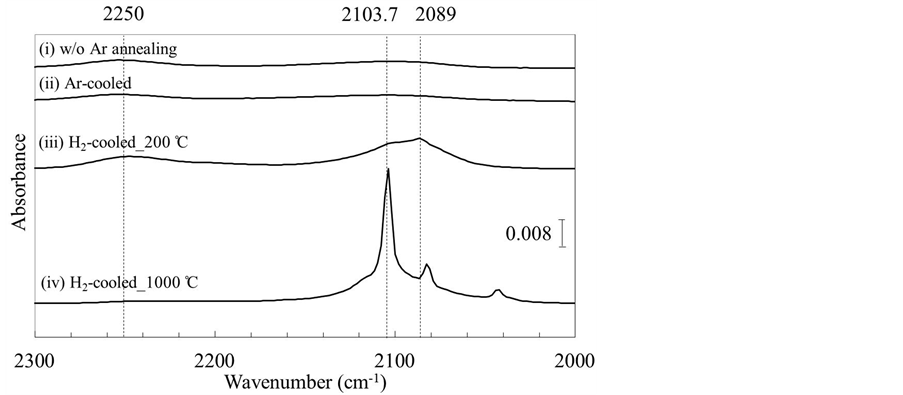
Figure 1. FT-IR-ATR spectra of Si(110) surfaces (i) before Ar annealing (w/o Ar annealing); (ii) after Ar annealing using Ar gas during cooling process (Ar-cooled); (iii) after Ar annealing using H2 gas during the cooling process from 200˚C (H2-cooled_200˚C); and (iv) after Ar annealing using H2 gas during the cooling process from 1000˚C (H2-cooled_1000˚C).
The peak at 2250 cm−1 is known to be caused by oxidation, and thus if oxidation is enhanced during the annealing process, the height/intensity of the 2250 cm−1 peak should increase. However, we found that the intensity of this peak was lowest for the H2-cooled_1000˚C sample. Therefore, a stable atomic surface obtained after high-temperature annealing can be improved by replacing Ar with H2 at 1000˚C during cooling. On the other hand, the H2-cooled_200˚C sample showed no clear difference from the Ar-cooled sample in terms of the 2250 cm−1 peak intensity.
Figure 2 shows the XPS spectra for annealed Si(110) wafers for the binding energy range of 98 - 104 eV. SiOx layers were observed on the Si(110) surfaces regardless of whether H2 or Ar was used during the cooling process. However, the SiOx peak intensities for the both H2-cooled samples were markedly lower than those for the Ar-cooled samples. Furthermore, the thickness of the SiOx layer was lower in the H2-cooled_1000˚C sample than in the H2-cooled_200˚C sample.
Figure 3 shows the oxide layer thicknesses calculated from the XPS spectra [18] . On Si(110) surfaces cooled in an Ar atmosphere, the oxide layer was 0.6 nm thick. In contrast, for H2-cooled samples, reflow oxidation was effectively suppressed, resulting in oxide layers with thicknesses of 0.4 nm for H2-cooled_200˚C sample and 0.2 nm for H2-cooled_1000˚C sample. These results are in approximate agreement with the aforementioned FT-IRATR observations.
Finally, we investigated the atomic surface structures of the samples by AFM. The surface morphologies of typical Si(110) wafers measured by AFM in an area of 3 × 3 μm2 are shown in Figure 4. The images for the polished Si wafer in Figure 4(i) were obtained from reference data. In contrast to a non-annealed surface, all Ar-annealed samples shown in Figures 4(ii)-(iv) had terrace and step structures, although the terrace width was slightly different in each Ar-annealed Si(110) sample. This difference in widths is tentatively attributed to the variation in the off-angles of the starting wafers [7] .
The H2-cooled_1000˚C sample (Figure 4(iv)) showed no obvious characteristic line-shaped oxidation as seen for the Ar-cooled sample (Figure 4(ii)), but the surface was observed to be somewhat rough. However, this somewhat rough surface became smoother with time, as confirmed by a second AFM measurement taken 30 min after the first one, as in our previous work [14] . No characteristic line-shaped oxidation of the Si(110) was observed in this second observation, either. This roughness variation only occurred for the H2-cooled_1000˚C sample. In contrast, characteristic line-shaped oxidation was observed for the H2-cooled_200˚C sample [Figure 4(iii)], as well as for the Ar-cooled sample. In addition, the somewhat rough surface caused by H2 gas etching of the H2-cooled_1000˚C sample was not seen on the H2-cooled_200˚C sample. The surface observed in the AFM images was in good agreement with the etching effect suggested by the FT-IR-ATR results.
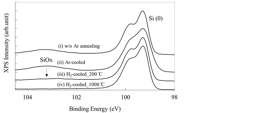
Figure 2. XPS spectra of Si(110) surfaces (i) before Ar annealing (w/o Ar annealing); (ii) after Ar annealing using Ar gas during the cooling process (Ar-cooled); (iii) after Ar annealing using H2 gas during the cooling process from 1000˚C (H2-cooled_1000˚C); and (iv) after Ar annealing using H2 gas during the cooling process from 200˚C (H2-cooled_200˚C).
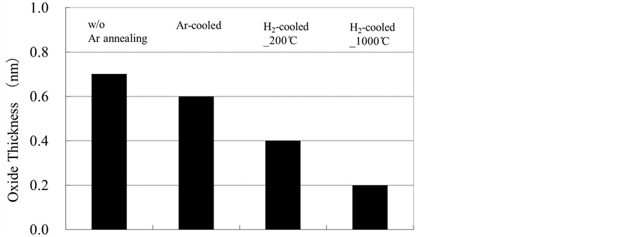
Figure 3. Thicknesses of oxide layers on Si(110) wafers calculated from XPS spectra.
Furthermore, we observed the roughness on the terrace in detail, as shown in the 0.2 × 0.2 μm2 view-field AFM images measured for one terrace on the Si(110) surface in Figure 5. The root mean square (rms) values of the surface roughness of the annealed Si(110) wafers along the lines drawn in the images are listed in the top panels in Figure 5.
When H2 was used during the cooling process from 1000˚C [Figure 5(iv)], the rms value was 0.048 nm, and the line-shaped oxidation was strongly suppressed. The differently colored region (lower left side) in Figure 5(iv) shows a different terrace. In contrast, the rms value when H2 was used during the cooling process from 200˚C was 0.098 nm because of the influence of the characteristic line-shaped oxidation, as shown in Figure 5(iii). The characteristic line-shaped oxidation on the terrace was more clearly observed in this measurement field. The maximum height on a terrace was 0.24 nm, which is almost same as that of Ar-cooled sample, although the surface structure might be slightly changed by the H2 gas etching.
On the basis of these results, the dependence of the atomic-scale Si(110) surface roughness on the hydrogen introduction temperature in high-temperature Ar annealing can be summarized as follows. Surface Si atoms migrate during high-temperature annealing at 1200˚C, and a reconstructed surface is considered to form during the cooling process below 800˚C [10] . It is assumed that the reconstructed Si(110) surface has a 16 × 2 structure that
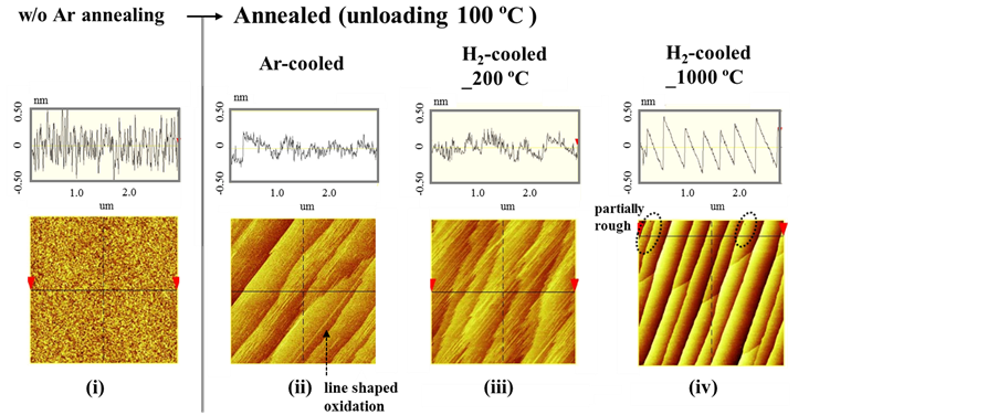
Figure 4. Surface roughness and AFM images of polished and annealed Si(110) wafers (images were obtained for a 3 × 3 μm2 measurement area) (i) before Ar annealing (w/o Ar annealing); (ii) after Ar annealing using Ar gas during the cooling process (Ar-cooled); (iii) after Ar annealing using H2 gas during the cooling process from 1000˚C (H2-cooled_1000˚C); and (iv) after Ar annealing using H2 gas during the cooling process from 200˚C (H2-cooled_ 200˚C).
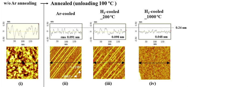
Figure 5. Surface roughness and AFM images of polished and annealed Si(110) wafers (images were obtained for a 0.2 × 0.2 μm2 measurement area) (i) before Ar annealing (w/o Ar annealing); (ii) after Ar annealing using Ar gas during the cooling process (Ar-cooled); (iii) after Ar annealing using H2 gas during the cooling process from 200˚C (H2-cooled_200˚C); and (iv) after Ar annealing using H2 gas during the cooling process from 1000˚C (H2-cooled_ 1000˚C).
is maintained when the sample is cooled to 100˚C in an Ar atmosphere. These reconstructed surfaces are atomically smooth but are chemically unstable. They are also unaffected by a reduction in the unloading temperature, but are easily oxidized by reflow oxidation during unloading. In particular, line-shaped oxidation occurs for Si(110) with a 16 × 2 surface structure after reconstruction because of preferential oxidation at the pentagonal pairs in the directions of Si[-112] and/or [-11-2], as described in [19] . This line-shaped oxidation causes a height fluctuation of approximately two atomic layers (0.24 nm) in AFM measurements, which hinders any decrease in Si(110) surface roughness.
When cooled in an H2 atmosphere, the reconstructed Si(110) surfaces are etched by H2 gas at a rate depending on the temperature. The etching rate of Si at 1000˚C is about 5 × 10⁻¹ nm/min [10] , and the pentagonal pairs that cause preferential oxidation in the Si[-112] and/or [-11-2] directions are effectively eliminated. Dangling bonds on the reconstructed surface, as well as broken dimer bonds and back bonds created by H2 gas etching, are terminated by hydrogen below 400˚C [16] . On the other hand, the etching rate of Si at 200˚C is estimated as less than 1 × 10⁻² nm/min [10] . The results obtained here obviously indicate that this temperature is too low for Si etching to eliminate the pentagonal pairs on the reconstructed Si(110) surface. As a result, the terminal H bonds are formed on the reconstructed surface, and preferential oxidation sites remain during the cooling process even under the H2 atmosphere. Nevertheless, the H-terminated reconstructed surface decreases the degree of reflow oxidation to approximately 70% (see Figure 3). However, line-shaped oxidation still immediately occurs through reflow oxidation upon unloading of sample, and thus the maximum height of the roughness on a terrace remains large. Therefore, we conclude that the preferential oxidation sites on the reconstructed structure must be eliminated by hydrogen etching in order to form an atomically smooth Si(110) surface.
Introducing H2 at 1000˚C entirely eliminates the preferential oxidation sites, and results in such an atomically flat surface. This technology has been utilized for evaluations of the performance of actual devices. For example, S. Jeon et al. verified the effect of the controlled surface using a MOSFET [20] . The results in this paper provide motivation for further such attempts. It would be possible to produce a high-mobility wafer with a high-quality gate oxide by very large scale integration (VLSI) fabrication by combining a technique for smoothing the surface atomic structure during annealing with a process for forming ultrathin oxidation layers.
4. Conclusion
We investigated the relationship between reflow oxidation and the structure of Si(110) surfaces by changing the H2 introduction temperature during the cooling process after high-temperature Ar annealing. The experimental results indicated that the maximum height of the roughness on reconstructed surface was not decreased at all when only slight Si etching occurred after hydrogen introduction at a lower temperature, even if H-termination occurred. The preferential oxidation sites need to be entirely eliminated in order to form atomically smooth Si(110) surfaces.
References
- Mack, C.A. (2011) Fifty Years of Moore’s Law. IEEE Transactions on Semiconductor Manufacturing, 24, 202-207. http://dx.doi.org/10.1109/TSM.2010.2096437
- Kish, L.B. (2002) End of Moore’s Law: Thermal (Noise) Death of Integration in Micro and Nano Elecronics. Physics Letters A, 305, 144-149. http://dx.doi.org/10.1016/S0375-9601(02)01365-8
- Okada, T., Takeda, R., Kubota, H. and Matsushita, Y. (2007) Surface Roughness Scattering Model Developments for p-MOS Monte Carlo Tool and Mobility Discussion about Wafer Orientation/Morphology. Proceedings of the 12th International Workshop on Computational Electronics (IWCE), 13-14.
- Fischetti, M.V. and Laux, S.E. (1993) Monte Carlo Study of Electron Transport in Silicon Inversion Layers. Physics Review B, 48, 2244. http://dx.doi.org/10.1103/PhysRevB.48.2244
- Hamada, T., Teramoto, A., Akahori, H., Nii, K., Suwa, T., Hirayama, M. and Ohmi, T. (2004) High Performance Low Noise CMOS Fabricated on Flattened (110) Oriented Si Substrate. IEICE Technical Report ED, 104, 41-44.
- Hasunuma, R., Okamoto, J., Tokuda, N. and Yamabe, K. (2004) Nonuniformity in Ultrathin SiO2 on Si(111) Characterized by Conductive Atomic Force Microscopy. Japanese Journal of Applied Physics, 43, 7861-7865. http://dx.doi.org/10.1143/JJAP.43.7861
- Zhong, L., Hojo, H., Matsushita, Y., Aiba, Y., Hayashi, K., Takeda, R., Shirai, H., Saito, H., Matsushita, J. and Yoshikawa, J. (1996) Evidence of Spontaneous Formation of Steps on Silicon (100). Physics Review B, 54, R2304-R2307. http://dx.doi.org/10.1103/PhysRevB.54.R2304
- Zhong, L., Hojo, H., Aiba, Y., Chaki, K., Yoshikawa, J. and Hayashi, K. (1996) Atomic Steps on Silicon (001) Surface Tilted toward an Arbitrary Direction. Applied Physics Letters, 68, 1823-1825. http://dx.doi.org/10.1063/1.116025
- Tokumoto, H. and Morita, Y. (1996) Structure of Hydrogen-Passivated Si surfaces Studied by STM. Hyomen Kagaku, 17, 516-522 [in Japanese]. http://dx.doi.org/10.1380/jsssj.17.516
- Kumagai, Y., Namba, K., Komeda, T. and Nishioka, Y. (1998) Formation of Periodic Step and Terrace Structure on Si(100) Surface during Annealing in Hydrogen Diluted with Inert Gas. Journal of Vacuum Science & Technology A, 16, 1775-1778. http://dx.doi.org/10.1116/1.581301
- Ohsawa, K., Kogure, Y., Araki, K., Isogai, H., Takeda, R., Matsushita, Y., Hasunuma, R. and Yamabe, K. (2008) Uniform Growth of Ultrathin SiO2 Films (2)—Roughness of Thermal Oxide Grown on Si(100) and Si(110) Surfaces, Ext. Abstr. 55th Spring Meeting 2008 of the Japan Society of Applied Physics and Related Societies, Chiba, 27-30 March 2008, 27a-X-4, 837 (in Japanese).
- Araki, K., Isogai, H., Takeda, R., Izunome, K., Matsushita, Y., Takahashi, N. and Zhao, X. (2009) Effect of Reflow Oxidation on Si Surface Roughness during High-Temperature Annealing. Japanese Journal of Applied Physics, 48, Article ID: 06FE05. http://dx.doi.org/10.1143/JJAP.48.06FE05
- Araki, N. (2009) Influence of Electrostatic Charge on Recombination Lifetime and Native Oxide Growth on HF-Treated Silicon Wafers. Japanese Journal of Applied Physics, 48, Article ID: 011201. http://dx.doi.org/10.1143/JJAP.48.011201
- Araki, K., Isogai, H., Takeda, R., Izunome, K., Matsushita, Y. and Zhao, X. (2010) Effect of Hydrogen Termination on Surface Roughness Variation of Si(110) by Reflow Oxidation during High-Temperature Ar Annealing. Japanese Journal of Applied Physics, 49, Article ID: 085701. http://dx.doi.org/10.1143/JJAP.49.085701
- Kimura, Y. and Niwano, M. (2001) Initial Stage of Etching of Si Electrode Surfaces Investigated by Surface Infrared Spectroscopy. Proceedings of the Electrochemical Society, 2000-25, 82-89.
- Kuge, J., Terashi, M. and Niwano, M. (1997) In-Situ IR Study of Hydrogen Adsorption on Si Surface. IEICE Technical Report SDM, 97, 25-30 (in Japanese).
- Akahori, H., Nii, K., Tsukamoto, K., Teramoto, A. and Ohmi, T. (2004) Control of Native Oxide Growth on Silicon Surface. IEICE Technical Report SDM, 187, 23-28 (in Japanese).
- Fujii, T. and Tanabe, M. (1990) Measurement of Film Thickness with XPS. Shimadzu Hyoron, 47, 89 (in Japanese).
- Suemitsu, M., Kato, A., Togashi, H., Kanno, A., Yamamoto, Y., Teraoka, Y., Yoshigoe, A., Narita, Y. and Enta, Y. (2007) Real-Time Observation of Initial Thermal Oxidation on Si(110)-16 × 2 Surfaces by O 1s Photoemission Spectroscopy Using Synchrotron Radiation. Japanese Journal of Applied Physics, 46, 1888-1890. http://dx.doi.org/10.1143/JJAP.46.1888
- Jeon, S., Taoka, N., Matsumoto, H., Nakano, K., Koyama, S., Kakibayasi, H., Araki, K., Miyashita, M., Izunome, K., Takenaka, M. and Takagi, S. (2013) Impacts of Surface Roughness Reduction in (110) Si Substrates Fabricated by High-Temperature Annealing on Electron Mobility in n-Channel Metal-Oxide-Semiconductor Field-Effect Transistors on (110) Si. Japanese Journal of Applied Physics, 52, Article ID: 04CC26. http://dx.doi.org/10.7567/JJAP.52.04CC26
NOTES

*Corresponding author.