Journal of Surface Engineered Materials and Advanced Technology
Vol.3 No.2(2013), Article ID:30789,5 pages DOI:10.4236/jsemat.2013.32017
Determination of the Nucleation Region Location of Si Nano-Crystal Grains Prepared by Pulsed Laser Ablation through Changing Position of Substrates
![]()
1College of Physics Science and Technology, Hebei University. Key Laboratory of Photo-Electronics Information Materials of Hebei Province, Baoding, China; 2Key Laboratory of Earthquake Geodesy, Institute of Seismology, CEA, Wuhan, China.
Email: hdwangyl@hbu.cn
Copyright © 2013 Zechao Deng et al. This is an open access article distributed under the Creative Commons Attribution License, which permits unrestricted use, distribution, and reproduction in any medium, provided the original work is properly cited.
Received January 6th, 2013; revised March 20th, 2013; accepted April 15th, 2013
Keywords: Nucleation Region Location; Si Nano-Crystal Grains; Pulsed Laser Ablation
ABSTRACT
To determine the nucleation region location of Si nano-crystal grains, pulsed laser ablation of Si target is performed in Ar gas of 10 Pa at room temperature with laser fluence of 4 J/cm2, the substrates are located horizontal under ablation spot with different vertical distance. Characteristics of deposited grains are described by scanning electron microscopy, Raman scattering and X-ray diffraction spectra, the results indicate that deposition position on substrates in a certain range is relative to target surface, which changes according to different vertical distance of substrates to ablation spot. Grain size increased at first and then decreased with addition of lateral distances to target in the range, but the integral distribution rule was independent of position of substrates. Combining with hydrodynamics model, nucleation division model, thermokinetic equation and flat parabolic motion, spatial nucleation region location of grains is obtained through numerical calculations, which is 2.7 mm - 43.2 mm to target surface along the plume axis.
1. Introduction
The films that contain Si nano-crystal grains are used widely in the area of micro-electronics, photo-electricity integration, solar cell [1-3] and biomedicine et al. following with the rapid progress of preparation technology [4,5], but the efficiency and property of many apparatus are limited for the size and uniformity of grains. These problems will be resolved successfully through preparing ideal size of grains, but the dynamics of nucleation and growth of grains is indistinct for us up to date. Naturally, study works about it become hot topic gradually in recent years [6-9]. Among the numerous study methods, pulsed laser ablation (PLA) get the most attention for its unique advantages such as rapid thermogenic speed, high atoms concentration and small surface contamination et al. On the selection of laser source, nanosecond (ns) and femtosecond (fs) laser are the most popular [10-13]. Different from nucleation mechanism of fs-laser ablation, the grains form through collision with ambient gas during ablated atoms transportation after ns-laser ablated targetand the processes of nucleation and growth are influenced synchronously by the parameters of laser fluence, laser frequence, extra force, sort and pressure of ambient gas, et al., which are convenient for researchers to investigate the dynamics from many different perspectives, so the method of ns-PLA has been adopted extensively for the past two decades. As the most important area for nucleation and growth of grains during process of ns-PLA, the nucleation region (NR) range directly determines the size and uniformity of formed grains [11]. That is to say, the determination of NR location will provide theory basis and reference for further study process of nucleation and growth dynamics of grains.
In order to avoid affection of external factors such as extra gas flow, electric field et al., Si nano-crystal grains are deposited on substrates that placed horizontal under ablation spot with different vertical distance (h) in this article, according to the experimental results of size and deposition location of grains, several kinetic equations of nucleation position are constituted, and the value of NR location is obtained by numerical calculation.
2. Experimental Details
Si target (resistivity is 3000 Ω·cm) is ablated by a focused laser beam(ablated area is 2 mm2) of XeCl (wavelength is 308 nm, pulse duration is 15 ns), and the target is rotated by a stepping motor at speed of 6 rpm. Chamber is filled with pure Ar gas (99.9999%) of 10 Pa after base pressure is evacuated less than 2 × 10⁻⁴ Pa. Films are deposited on two different substrates, namely glass plates and Si(111). Which are located horizontal under ablation spot. The vertical distances h are 1.5 cm, 2.0 cm and 2.5 cm, respectively. Laser fluence is 4 J/cm2 and pulse frequency is 1 Hz during experiments. All films (thickness: 200 nm) are prepared at room temperature. Samples deposit on glass plates are analyzed by Raman scattering (Raman: MKI-2000) and X-ray diffraction spectra (XRD: 12 kW, Cuka Radiation), while samples deposit on Si(111) substrates are characterized by scanning electron microscopy (SEM: JSM-7500F).
3. Experimental Results
The statistical results of size and positional distribution of deposited grains with different h are shown as Figure 1, which indicate that the size of grains are almost same not only at two tends of deposition range but also at the maximum with different h, and the change rule of grain size are same, which increase at first and then decrease with addition of lateral distances to target. The only difference is deposition range move away target with addition of h under the condition of width unchanged. Here, the results of h = 2.5 cm are selected out as typical representation, which are analyzed detailed in the following content.
SEM graphs of films are shown in Figures 2(a)-(h) corresponding to the various deposition location to target surface of 5.4 mm, 5.5 mm, 11.0 mm, 16.0 mm, 26.0

Figure 1. Statistical result of size and deposition of grains on substrates with different h.
mm, 36.0 mm, 45.6 mm and 45.7 mm, respectively. It is obviously that no grains can be found on (a) and (h) graphs, results of Raman and XRD of films deposited on the glass plates at the same position indicate they are amorphous too. That is to say, 5.5 mm and 45.6 mm are initial and end position of grains detected on substrates respectively.
Raman and XRD spectra of films on glass plates with the same deposited position of 5.5 - 45.6 mm as SEM are demonstrated in Figures 3 and 4. In Figure 3, the corresponding main peaks of spectra are 516.488 cm–1, 518.981 cm–1, 519.474 cm–1, 517.502 cm–1, 515.502 cm–1 and 514.009 cm–1, respectively. They all close to the characteristic peak of single crystal Si of 520 cm−1, which prove that grains are crystalline. At the same time, the main peaks of spectra first right shift and then left shift indicates the size of grains increase at first and then decrease by equation of d = 2π(B/ω)1/2 [14], which agree with statistic operation of SEM. In the frontal formula, d represents the diameter of grain, ω is the peak shift for the grains as compare to c-Si, B = 2.0 cm–1·nm2. Additionally, the peaks at around 28.4˚ of XRD in Figure 4 corresponding to crystal Si(111), which reveals the crystalline grain are produced too. And the FWHM of spectra are 0.174˚, 0.151˚, 0.137˚, 0.165˚, 0.186˚ and 0.199˚, which become narrow at first and then broaden prove the change rule of grain size consistent with statistical results of SEM and Raman by Scherrer formula d = kλ/βcosθ [15]. Where d represents the diameter of grain, k is the factor of the crystal figure, λ is the wavelength of the X-ray, and θ is the diffraction angle, β is equal to (B2 – b02)1/2, where B is the width at half-tallness of the diffraction peak and b0 is the broadening factor of the instrument.
4. Theory Analysis and Calculation of NR Location
The main process of grain formation is vapor nucleation as background gas at room temperature. Ablated Si atoms with high energy spray from target after laser ablation, kinetic energy of atoms wear down through collision with background gas during transportation, slowing coefficient of ablated Si atom in background gas is aSi = CSSiρ/2 [16], in which C is proportional constant, SSi is cross section of Si atom, and ρ is the ambient gas density. The cohesive energy of grain is offered by the lost kinetic energy of ablated atoms. Under the condition of supersaturation, when thermal motion temperature of atoms under the melting point of single crystal Si, the nucleation phenomenon will happen [11], namely, grains form in a region scale apart from target, outside the
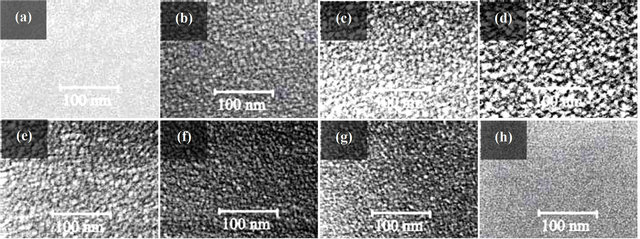
Figure 2. SEM graphs of samples.
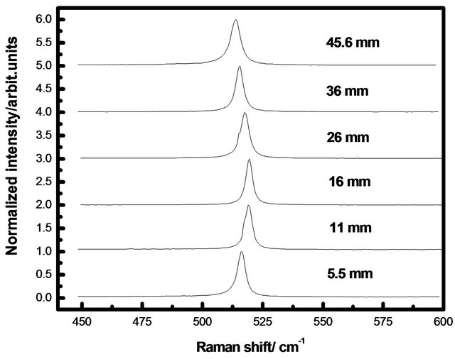
Figure 3. Raman spectra of samples.

Figure 4. XRD spectra of samples.
context of this range, there are no grains, which could be due to the temperature or density or both of them of Si atoms do not satisfy the nucleation condition [17]. Thermodynamics equation is . kB is Boltzmann constant, T is nucleation thermal motion temperature for ablated atoms, mSi and mΔ are mass of Si atom and formed grain, vSi and vΔ are velocity of nucleated atoms and formed grains respectively, which are assumed parallel to substrates here. A is energy conversion coefficient between ablated atoms and grains, the formed grains in space will deposit onto the substrates through flat parabolic motion under the effect of gravity (g).
In this article, the plume is assumed limited in the cylinder with ablation spot as area of base. On the base of experimental results, the mean size of grains deposited increase at first, and then decrease with addition of lateral distance from target surface, which is caused by the velocity distribution rule of ablated atoms. According to the results of numerical simulation, velocity of ablation atoms is Maxwell distribution under a single pulsed laser, which is maximum at front of plume and minimum near target, furthermore, the number of these two parts are fewer than those atoms with velocity near the value of most probable velocity. Basing on the frontal thermodynamics formula, low thermal motion temperature of atoms corresponding to small velocity, so the temperature will reach to nucleation condition [11] first through collision with ambient gas, that is to say, nucleation will happen first naturally near target, which was approved by the experimental results of Makimura [18,19]. Obviously, high temperature corresponding to greater velocity, these atoms need to experience more collisions before nucleation, so the nucleation position is comparative farther to target surface in constant gas pressure. For the number and density [20] of atoms with velocity close to the most probable velocity is much more, so the grains formed by these atoms have bigger growth probability, which cause the bigger grains, thus the size of grains increase at first to a maximum, and then decrease with addition of lateral distance from target surface.
The schematic diagram of nucleation and motion for grains is shown in Figure 5.
x0 is position of grains formation in the space, x represents its deposition location on substrates, v0Si is initial velocity of ablated atoms, which parallel to substrates

Figure 5. Schematic diagram of vapor nucleation and transportation of grain
too.
In order to calculate conveniently, the size of grains deposit on substrates is assumed the value of initial formation at the height of h. During transportation process, collision section of Si and Ar atoms is SSi-Ar = π(rAr + rSi)2, SΔ-Ar = π(rAr + rΔ)2 corresponding to grain, rAr, rSi and rΔ are radius of Si atom, Ar atom and formed grain, respectively. Through hydrodynamics model of Yoshida [16] and flat parabolic motion of grains, formulas about spatial position of grain formation are gotten
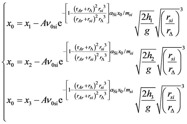
mSi = 4.67 × 10⁻²⁶ kg, rSi = 1.46 × 10⁻¹⁰ m, rAr = 8.8 × 10⁻¹¹ m, and v0Si = 1760 m/s [21] are used. There are three equations corresponding to three different h, so the equation group that including three formulas is established. Results of calculation show that the initial and end NR location is 2.7 mm to 43.2 mm, so the NR width is 40.5 mm, and A = 6.1 × 10⁻³, aSi = 2.05 × 10⁻²⁴ kg/m.
5. Conclusion
In conclusion, we have prepared Si nano-crystal grains by pulsed laser ablation at room temperature without introducing any external force, grains deposit on the substrates in a certain range, mean size increase at first and then decrease in this range with addition lateral distance from target surface. The experimental results are explained reasonably on the base of hydrodynamics model, nucleation division model and thermokinetic equation. Spatial nucleation region location is obtained through setting up and solving equation group, which is 2.7 mm - 43.2 mm to target surface along the plume axis. At the same time, the value of energy conversion coefficient of A and slowing coefficient of aSi are obtained. This may pave a way for investigating concretely the dynamics of nucleation and growth process for Si grains and preparing high quality crystalline films.
6. Acknowledgements
Project supported by the special Foundation of State Key Development Program for Basic Research of China (2011CB612305), the NSF of Hebei Province (E2011201134, E2012201035) and the Research Project of Colleges and University of Hebei Province (Q2012084), China.
REFERENCES
- K. Kim, J. H. Park, S. G. Doo, J. D. Nam and T. Kim, “Generation of Size and Structure Controlled Si Nanoparticles Using Pulse Plasma for Energy Devices,” Thin Solid Films, Vol. 517, No. 14, 2009, pp. 4184-4187. doi:10.1016/j.tsf.2009.02.016
- E. C. Cho, S. W. Park, X. J. Hao, D. Y. Song, G. Conibeer, S. C. Park and M. A. Green, “Silicon Quantum Dot/ Crystalline Silicon Solar Cells,” Nanotechnology, Vol. 19, No. 24, 2008, pp. 245201-245205. doi:10.1088/0957-4484/19/24/245201
- S. H. Hong, J. H. Park and D. H. Shin, “Dopingand Size-Dependent Photovoltaic Properties of p-Type SiQuantum Dot Heterojunction Solar Cells: Correlation with Photoluminescence,” Applied Physics Letters, Vol. 97, No. 7, 2010, pp. 072108-1-072108-3. doi:10.1063/1.3480609
- Z. Ouyang, S. Pillai, F. Beck, O. Kunz, S. Varlamov, K. R. Catchpole, P. Campbell and M. A. Green, “Effective Light Trapping in Polycrystalline Silicon Thin-Film Solar Cells by Means of Rear Localized Surface Plasmons,” Applied Physics Letters, Vol. 96, No. 26, 2010, pp. 261109-1-261109-3. doi:10.1063/1.3460288
- K. Irina, I. Teodora, M. Mihaela, C. Florea, T. Mihaela, S. Monica, B. Adina and D. Adrian, “Nanostructured Silicon Particles for Medical Applications,” Journal of Nanoscience and Nanotechnology, Vol. 10, No. 4, 2010, pp. 2694-2700. doi:10.1166/jnn.2010.1419
- S. R. Franklin and R. K. Thareja, “Simulation of Cluster Formation in Laser-Ablated Silicon Plumes,” Journal of Applied Physics, Vol. 97, No. 12, 2005, pp. 123303-1- 123303-6. doi:10.1063/1.1931028
- I. Umezu and A. Sugimura, “Formation of Nanoscale Fine-Structured Silicon by Pulsed Laser Ablation in Hydrogen Background Gas,” Physics Review B, Vol. 76, No. 4, 2007, pp. 045328-1-045328-10. doi:10.1103/PhysRevB.76.045328
- Y. Khang and J. Lee, “Synthesis of Si Nanoparticles with Narrow Size Distribution by Pulsed Laser Ablation,” Journal of Nanoparticle Research, Vol. 12, No. 4, 2010, pp. 1349-1354. doi:10.1007/s11051-009-9669-z
- F. Ratto, A. Locatelli, S. Fontana, S. Kharrazi, S. Ashtaputre, S. K. Kulkarni, S. Heun and F. Rosei, “Diffusion Dynamics during the Nucleation and Growth of Ge/Si Nanostructures on Si(111),” Physics Review Letters, Vol. 96, No. 9, 2006, pp. 096103-1-096103-4. doi:10.1103/PhysRevLett.96.096103
- R. Glaus, R. Kaegi, F. Krumeich and D. Günther, “Phenomenological Studies on Structure and Elemental Composition of Nanosecond and Femtosecond Laser-Generated Aerosols with Implications on Laser Ablation Inductively Coupled Plasma Mass Spectrometry,” Spectrochimica Acta Part B: Atomic Spectroscopy B, Vol. 65, No. 9-10, 2010, pp. 812-822. doi:10.1016/j.sab.2010.07.005
- G. S. Fu, Y. L. Wang, L. Z. Chu, Y. Zhou, W. Yu, L. Han and Y. C. Peng, “The Size Distribution of Si Nanoparticles Prepared by Pulsed-Laser Ablation in Pure He, Ar or Ne Gas,” Europhysics Letters, Vol. 69, No. 5, 2005, pp. 758-762. doi:10.1209/epl/i2004-10420-2
- Y. L. Wang, Z. C. Deng, L. Z. Chu, G. S. Fu and Y. C. Peng, “The Difference of Energies of Si Atoms with Single-Crystalline, Amorphous, Free and Nanoparticle Configurations,” Europhysics Letters, Vol. 86, No. 1, 2009, pp. 15001-15005. doi:10.1209/0295-5075/86/15001
- S. Amoruso, R. Bruzzese, X. Wang and J. Xia, “Propagation of a Femtosecond Pulsed Laser Ablation Plume into a Background Atmosphere,” Applied Physics Letters, Vol. 92, No. 4, 2008, pp. 041503-1-041503-3. doi:10.1063/1.2839582
- J. Zi, H. Büscher, C. Falter, W. Ludwig, K. M. Zhang and X. D. Xie, “Raman Shifts in Si Nanocrystals,” Applied Physics Letters, Vol. 69, No. 2, 1996, pp. 200-202. doi:10.1063/1.117371
- A. L. Patterson, “The Scherrer Formula for X-Ray Particle Size Determination,” Physics Review, Vol. 56, No. 10, 1939, pp. 978-982. doi:10.1103/PhysRev.56.978
- T. Yoshida, S. Takeyama, Y. Yamada and K. Mutoh, “Nanometer-Sized Silicon Crystallites Prepared by Excimer Laser Ablation in Constant Pressure Inert Gas,” Applied Physics Letters, Vol. 68, No. 13, 1996, pp. 1772- 1774. doi:10.1063/1.116662
- Z. C. Deng, Q. S. Luo, X. C. Ding, L. Z. Chu, W. H. Liang, J. Z. Chen, G. S. Fu and Y. L. Wang, “Pressure Threshold and Dynamics of Nucleation for Si NanoCrystal Grains Prepared by Pulsed Laser Ablation,” Acta Physics Sinica, Vol. 60, No. 12, 2011, pp. 126801-1- 126801-5.
- T. Makimura, T. Mizuta and K. Murakami, “Formation Dynamics of Silicon Nanoparticles after Laser Ablation Studied Using Plasma Emission Caused by Second-Laser Decomposition,” Applied Physics Letters, Vol. 76, No. 11, 2000, pp. 1401-1403. doi:10.1063/1.126045
- T. Makimura, T. Mizuta, T. Takahashi and K. Murakami, “In Situ Size Measurement of Si Nanoparticles and Formation Dynamics after Laser Ablation,” Applied Physics A, Vol. 79, No. 4-6, 2004, pp. 819-821. doi:10.1007/s00339-004-2798-4
- S. S. Harila, C. V. Bindhu, M. S. Tillack, F. Najmabadi and A. C. Gaeris, “Internal Structure and Expansion Dynamics of Laser Ablation Plumes into Ambient Gases,” Journal of Applied Physics, Vol. 93, No. 5, 2003, pp. 2380-2388. doi:10.1063/1.1544070
- Y. L. Wang, Y. L. Li and G. S. Fu, “Relation between Size-Distribution of Si Nanoparticles and OscillationStabilization Time of the Mixed Region Produced during Laser Ablation,” Nuclear Instruments and Methods in Physics Research Section B: Beam Interactions with Materials and Atoms, Vol. 252, No. 2, 2006, pp. 245-258. doi:10.1016/j.nimb.2006.09.006