Journal of Crystallization Process and Technology
Vol.08 No.04(2018), Article ID:92178,18 pages
10.4236/jcpt.2018.84006
Fluorine-Doped Tin Oxide Thin Films Deposition by Sol-Gel Technique
Amel Adjimi1, Meryem Lamri Zeggar1,2, Nadhir Attaf1, Mohammed Salah Aida3,4*
1Laboratoire Couches Minces et Interfaces, Université des Frères Mentouri Constantine 1, Constantine, Algeria
2Ecole Normale Supérieure de Constantine, Constantine, Algerie
3Department of Physics Faculty of Science King Abdulaziz University, Djeddah, KSA
4Center of Nanotechnology King Abdulaziz University, Djeddah, KSA

Copyright © 2018 by author(s) and Scientific Research Publishing Inc.
This work is licensed under the Creative Commons Attribution-NonCommercial International License (CC BY-NC 4.0).
http://creativecommons.org/licenses/by-nc/4.0/


Received: August 30, 2018; Accepted: October 28, 2018; Published: October 31, 2018
ABSTRACT
In the present work, undoped (SnO2) and fluorine-doped tin oxide (FTO) thin films were prepared by sol-gel process using a solution composed of (SnCl2, H2O), (NH4F), and ethanol mixture. The fluorine concentration effect on structural, optical and electrical properties of SnO2 films is investigated. The electrical properties of FTO films prepared by sol gel remain relatively lower than the ones deposited by other techniques. In present paper, we try to elucidate this difference. Films composition and the FTIR analysis, of films and formed precipitate during film growth, indicate that few amounts of fluorine are incorporated in SnO2 network, most of fluorine atoms remain in the solution. The films resistivity is reduced from 1.1 Ω・cm for undoped films to 3 × 10⁻² Ω・cm for 50 wt.% doped FTO, but remains higher than the reported ones in the literature. This high resistivity is explained in terms of fluorine bonding affinity in the solution.
Keywords:
Transparent Conducting Oxide, Thin Films, Sol-Gel

1. Introduction
Doped tin oxide thin films have succeeded as leading candidates for uses as transparent conducting oxides (TCO) [1] . They have been extensively investigated. SnO2 thin films exhibit high optical transparency (T ≥ 85%) and a large n-type electrical conductivity that can be tailored by doping with foreign atoms [2] . The most favored doping atoms are indium (In) and antimony (Sb) which substitute tin cations or fluorine (F) substituting the oxygen [2] . Fluorine-doped tin oxide (FTO) has good transparency, in the visible range, due to its wide band-gap (Eg > 3 eV) and a low electrical resistivity due to the large free carriers concentration caused by oxygen vacancies and fluorine substitution [3] . FTO is chemically stable [4] . It found several technological applications including; solar cells [5] , low emissivity coatings for windows [6] , gas sensors [7] , and liquid crystal displays [8] . Several methods were used for FTO films deposition such as: chemical vapor deposition (CVD) [9] [10] , sputtering [11] [12] [13] , plasma evaporation [14] , ultrasonic spray pyrolysis (USP) [15] [16] and sol-gel method (spin or dip coating) [17] [18] . Sol-gel process is more advantageous than the other methods due to its low-cost, simplicity and the possibility of films deposition onto large and complex shaped substrates. However, the electrical properties of FTO films prepared by sol-gel remain relatively lower than the ones deposited by other techniques. In the present paper, we try to elucidate this difference. For this purpose, un-doped and fluorine-doped tin-oxide SnO2 thin films were prepared by sol-gel dip coating process. The effects of fluorine doping rate SnO2 films properties are studied. In order to investigate the fluorine presence, we have analyzed the composition of FTO film and the formed powder in the solution during film growth.
2. Experimental Details
2.1. Solutions and Thin Film Deposition
Undoped and F doped SnO2 films were deposited on microscopic glass substrates by sol-gel method using dip-coating technique. The salt precursor (SnCl2・2H2O) was dissolved into 5 ml of hydrochloric acid (HCl) and heated at 60˚C for 10 min. 25 ml of ethanol was added to obtain a solution of 0.1 M. In order to promote the gel formation, some drops of Triethanolamine (TEA) are added to the prepared solution. The added NH4F into pre-mixed solution is the source of fluorine doping atoms. The resulting solutions were stirred for 2 hours at 60˚C, a clear and homogeneous solution was obtained, it was left to age for 24 h at room temperature resulting in a gel-like structure. The immersed glass substrates were withdrawn vertically from the solution at the rate of 8 cm/min. For film formation with suitable thickness, 15 dipping were repeated, between two successive dipping the deposited films were dried at 100˚C and finally annealed at 450˚C in air for 90 minutes.
2.2. Characterizations
Films structural properties were determined by XRD using Philips X’Pert system under CuKα (λCu = 0.154056 nm) radiation whereas the 2θ scanning range was between 20˚ and 80˚. The films’ composition and morphology were determined by using various measurements: energy-dispersive X-ray spectroscopy (EDS) with the electron-beam energy set to 7 keV. The micro-Raman measurements were performed using a Renishaw Raman spectrometer. Fourier transformation infrared (FTIR) spectra were recorded using a Perkin-Elmer 2000 spectrometer. The optical transmission in the UV-visible range (200 - 900 nm) measurements was performed using Shimadzu UV-3101PC spectrophotometer. Films thicknesses and optical band gaps were deduced from optical transmission data fitting. The thickness calculation procedure is based on the comparison between the experimental transmittance data with the theoretical one calculated using Swanepoel theory [19] , where film thickness and refractive index are varied till convergence. The films electrical properties were studied by two probes method measurements in dark and at room temperature, in a coplanar structure formed by two golden strips electrodes deposited by DC sputtering onto films surface.
3. Results and Discussion
3.1. Structural Properties
The X-ray diffraction spectra of FTO films prepared with different fluorine doping levels in the precursor solution are shown in Figure 1. As can be seen, all films are polycrystalline with (110) preferred growth orientation except the one deposited with 10 wt.% F which exhibits an amorphous state. The strong (110) peak is accompanied by other peaks such as (101), (200), (220) and (211) but with substantially lower intensities, confirms the tetragonal structure of the prepared SnO2 films (JCPDS N˚. 41-1445) [20] . As seen, the introduction of fluorine in SnO2 network does not affect its structure but it reduces the peak intensities probably due to the reduction of film thickness. Small peak located at 31.77˚ assigned to the (111) direction of SnO2 cubic phase ((JCPDS 50-1429) is detected in films a and c (Figure 1). The same remark has been reported by Keskenler et al. [21] . in tungsten and fluorine co-doped SnO2 prepared by sol-gel technique.

Figure 1. XRD pattern of: (a) un-doped; (b) 10 wt.% F doped; (c) 40 wt.% F doped; (d) 50 wt.% F doped SnO2 films; (e) from JCPDS card N˚. 41-1445.
To evaluate the preferred growth direction, the texture coefficient TC(hkl) for each direction (hkl) was estimated using the following formula [22] .
(1)
where I(hkl) and I0(hkl) are respectively the measured and the standard intensity in the JCPDS card of the plane (hkl) and n is the reflection. The larger the deviation of texture coefficient from unity, the higher will be the preferred orientation.
The variation of texture coefficient estimated along (110), (101) and (211) directions with the fluorine content for SnO2:F thin films are listed in Table 1. As can be seen, the direction (110) remains the preferential orientation in undoped or doped SnO2, the same conclusion has been reported by several authors [23] [24] [25] .
The lattice constants “a” and “c” were determined from XRD results using the equation [26] :
(2)
where dhkl is the inter-planar distance, (hkl) are the Miller indexes. As reported in Table 1, the calculated values are in agreement with the standard data (a0 = 4.738 Å, c0 = 3.187 Å). No notable change was observed with increasing F ion concentration, this may be due to the comparable ionic radius of F− (1.17 Å) to O−2 (1.22 Å).
The films crystallite size and internal lattice strain given in Table 1 have been estimated from Hall-Williamson equation [27] expressed as:
(3)
where β is the FWHM (full wide that half-maximum) of diffraction peaks, θ is the Bragg angle, λ is the X-rays wavelength, D is the crystallite size and ε is the internal strain. D and ε are estimated from the fit of the plot βcos(θ)/λ versus sin(θ)/λ calculated for different peaks. The crystallite size is deduced from the plotted intercept with the y-axis yields to, while the strain is equal to the slope of the plot as reported in Figure 2.

Table 1. Crystallite size, internal strain, lattice parameter a, c, and TC(hkl) of FTO thin films prepared with different doping levels of fluorine.

Figure 2. Hall-Williamson-plot used for the calculation of the crystallite size and strain in different films; (a) un-doped, (b) 40 wt.% doped and (c) (50 wt.%) doped SnO2:F.
The variations of the crystallite size and the internal strain are reported in Figure 3. Increasing fluorine content reduces the crystallite size from 25 to 12.5 nm and enhances the internal strain in the film network. The same trend has been reported by several authors [28] . In general, it is reported that introduction of doping atoms reduces the crystallite size regardless the host network such as ZnO, TiO2, SnO2 [29] [30] [31] . This may originate from the early stage of nucleation during film growth, actually, any foreign atom acts as a nucleation center, therefore the nucleation centers is increased in doped films causing the reduction of crystallite size.
3.2. Fourier Transform Infrared Analysis
The FTIR spectra of un-doped and F-doped SnO2 films are illustrated in Figure 4. The spectrum is formed with several absorption peaks assigned to Vibrational modes of SnO2 confirming its formation. The obtained spectra are comparable to the reported ones in the literature [32] [33] .
Peaks at low wave numbers (500 - 1000 cm−1) can be attributed to SnO2. For the un-doped film, the peaks located at 675 and 780 cm−1 were assigned to O-Sn-O and Sn-O stretching vibrations modes, respectively [34] .
An additional peak located at 804 cm−1, which becomes inconspicuous as fluorine concentration increases can be assigned to oxygen vacancies (V2+ ) presence in the O-Sn-O group. The oxygen vacancies modify the symmetrical O-Sn-O group to O-Sn- resulting in the weakening of O-Sn-O vibration due to the different bond lengths (O-Sn-O: 2.597 Å, Sn-O: 2.053 Å) [35] . Moreover, it is interesting to note that a weak peak near 408 - 410 cm−1 is observed in highly fluorine doped films. This peak is assigned to Sn-F vibration frequency

Figure 3. Crystallite size and internal stress in grain as a function of Fluorine concentration.

Figure 4. FTIR spectra of un-doped and F-doped SnO2 films.
[35] [36] . This indicates that few amounts of fluorine are introduced in SnO2 film despite the large ratio of fluorine in the starting solution. The absence of this peak in un-doped one and in F (10 wt.%) doped SnO2 films suggests that fluorine atom is not incorporated in SnO2 network at low doping level which is confirmed by EDS analysis.
The vibration frequencies of O-Sn-O display a shift from 780 to 760 cm−1 and a decrease in the intensity with fluorine concentration increase in the solution as shown in Figure 5. This shift can be ascribed to the increase in lattice deformation due to the interstitial fluorine ions in the lattice. Doping could allow the fluoride ions to occupy beside the oxygen sites, the interstitial positions,

Figure 5. Variation of Sn-O bond peak intensity and position with fluorine concentration.
causing a disorder in the film network this is confirmed by the optical measurements.
The formation of undoped and F doped SnO2 films might be achieved through the following reactions [37] [38] :
・In the solution:
・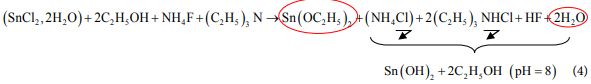
・ For un-doped SnO2 deposition:
(5)
An analysis of the precipitate, formed in the bath during solution film formation, was performed by FTIR spectroscopy, in order to investigate the fluorine atoms presence in the solution and in SnO2 lattice and to have an insight about the favorable fluorine bonding in the solution or in the film. Therefore, the precipitate resulted from solution contained 40 wt.% fluorine was analyzed by infrared spectroscopy.
The FTIR spectrum of this powder is reported in Figure 6. Strong peaks located at 1250, 1745 and 3540 cm−1 attributed to H-F bond vibration modes [39] are present in the spectrum indicating that a large amount of fluorine remains in the solution and do not incorporate in the solid film. In addition, according to the formation enthalpy of H-F and Sn-F bonds, that are respectively = −569.7 and −476.7 Kj/mol, H-F is easily formed than Sn-F. Hence the affinity of fluorine to bonding hydrogen in solution is larger than to bonding tin (Sn) in films. Consequently, little quantity of fluorine ions is incorporated in the films

Figure 6. FTIR spectra of precipitate formed during film growth.
during dip coating deposition. Moreover, the formation of FTO depends also on the mobility of fluorine ions in the solution and its availability on the reacting substrate surface. Thereafter, this explains, the absence of fluorine in films at low doping level and the inferiority of the electrical conductivity in FTO films prepared by sol-gel by comparison to the other techniques as mentioned below.
Several bands assigned to the compound NH4Cl are present in the spectrum [40] this confirm the formation of this compound according to the reaction (4).
3.3. Raman Scattering Analysis
Raman scattering is generally used to investigate the material crystallinity, structural defects and side effects of crystallites. Raman spectrum of unhoped and F-doped SnO2 thin films are shown in Figure 7 presents the room temperature. As can be seen, three fundamental Raman peaks located at 634, 475 cm−1 correspond respectively to A1g and B2g models are present in the different spectrum, they are assigned to the symmetric and asymmetric stretching of Sn-O bonds [40] , these are reported in the literature [41] [42] . The appearance of these modes confirms the cassiterite tetragonal structure of SnO2 as deduced from XRD analysis [43] . A shift in the A1g mode towards the lower wave number, accompanied with broadening of the Raman bands is observed in SnO2:F, could arise from the strain in the crystallite [44] and the disorder in the film network. This suggests that the fluorine incorporation is accompanied by the disorder formation in the film structure as confirmed as well by the shift of the O-Sn-O vibration frequency in FTIR spectrum.
3.4. Compositional Analysis
Compositional analysis of the elements present in the films was performed on different samples; a typical recorded EDS spectrum is shown in Figure 8. In

Figure 7. Raman spectrum of: (a) un-doped, (b) 10 wt.% doped, (c) 40 wt.% doped and (d) (50 wt.%) doped SnO2:F.

Figure 8. Typical EDS spectrum of SnO2:F thin films (film doped with 10 wt.% as an example).
Table 2 we have reported the elementary composition of different films. The most important feature is the absence of fluorine in supposed 10 wt.% F doped SnO2. While at higher doping level 40 wt.%, few amounts of fluorine is incorporated in SnO2 films network. This indicates that the fluorine was successfully incorporated into the tin oxide network but with a small amount. It is worth noting that the fluorine content in the films was very low compared with the initial percentage in the starting solution. This is due, as suggested from FTIR analysis, to the segregation of fluorine and its preference to remain in the solution rather than to be introduced in the film network. The amount of oxygen in the films is overestimated due to the oxygen originating from the glass substrate. However,
Table 2. EDS compositional analysis of the FTO films.
the alkali elements, such as Ca, K, Mg, Na and Si originate from the used glass substrate due to the low film thickness.
3.5. Optical Properties
The optical transmission spectra of FTO films deposited with different fluorine concentrations are shown in Figure 9. The average transmittance in the visible range was reduced from 65% to 60% with increasing the doping level. A shift in the absorption edge towards the higher photon energy was observed with fluorine doping at (40 wt.%), this may be attributed to the Burstein-Moss shift due to the increase in free electrons concentration [45] [46] [47] .
Films optical band gaps are estimated, as shown in Figure 10, from the plot of (αhν)2 versus photon energy (hν), according to Tauc formula for direct band gap semi-conductors [48] :
(6)
where α is the absorption coefficient, B is a constant, h is Planck’s constant, Eg is the energy band gap and ν is the photon frequency.
Due to the disorder in film network, localized states appear near the bands edges causing band tails formation. The states are responsible for the low energy photons absorption. The absorption coefficient in the band tail expressed as [49] :
(7)
where α0 is the pre-exponential factor, hν the photon energy and E00 ( known also as Urbach energy) is the bandtail energy width [50] . E00 is estimated from the inverse slope of ln(α) versus (hν) linear plot.
The direct band-gap values obtained in this work are ranged from 3.3 to 3.7 eV (Table 3), this is approximately the same values reported in [51] - [56] . Figure 11 shows the variations of the band gap and band tail width E00 with various fluorine doping levels. The Urbach energy rises with fluorine doping indicating that doping atoms induce disorder in films network [50] . This is consistent with band broadening observed in Raman spectra (Figure 7) and the strain increase with fluorine concentration as reported in Table 1. An increase in E00 causes the optical band gap shrinking. This suggests that the optical gap is controlled by the disorder in the film network rather than by free electrons due to the doping effect.

Figure 9. UV-visible transmittance spectrum of un-doped and doped fluorine SnO2 thin films deposited with different concentration of (F). Figure insert variation shows the absorption edge shift.

Figure 10. Typical variation of (ahν)2 as a function of photon energy used for optical band gap determination.
3.6. Electrical Properties
The electrical properties of films were characterized by tow probes technique. The results are reported in Table 3 and Figure 12, they are comparable to the reported ones in films prepared by sol-gel technique [24] [25] . Clearly, the resistivity decrease, by two orders of decade, with increasing F-doping levels as shown in (Figure 12). This reduction confirms the incorporation of fluorine in tin oxide; each F− anion substitutes an O2− anion in the lattice. This yields to an

Figure 11. Variation of optical band gap and disorder in film network as a function of Fluorine doping ratio.

Figure 12. Variation of resistivity of FTO films with fluorine doping concentration at different fluorine concentration.
Table 3. Electrical and optical characteristics of FTO thin films deposited with varied fluorine doping concentration.
increase in free electrons concentration and to a decreases in films resistivity. However, as reported in Table 4, the resistivity of FTO films prepared by sol-gel is relatively high by comparison to their values in the ones prepared by other techniques. This discrepancy is mainly due to the low amount doping fluorine hosted in the SnO2 network as concluded from Infrared spectroscopy and films composition analysis.
Once the electrical resistivity and the optical transmission T of films are known, the figure of merit can be calculated using Haacke’s equation [52] :
(8)
where Rsh is sheet resistance defined as the film resistivity divided by the film thickness. The obtained figure of merit values at different wavelengths are reported in Table 5. These values are close to the reported ones in sol-gel deposited FTO [53] .
Table 4. Comparison of the electrical resistivity of tin oxide thin films deposited by several techniques.
Table 5. Variation of figure of merit of FTO thin films deposition as a function of fluorine doping concentration.
4. Conclusion
In this paper, we have investigated the influence of fluorine doping of SnO2 thin films prepared using dip coating sol-gel method. The XRD analysis has confirmed the polycrystalline structure of SnO2 phase with (110) as a preferred orientation. FTIR and Raman spectroscopy confirm SnO2:F films formation. Both EDS films composition results and FTIR analysis of films and the precipitate during film growth confirm the relatively low amount of fluorine in SnO2 films by comparison to its amount in the starting solution. This suggests that fluorine ions remain mainly in solution to bond with other atoms especially hydrogen only few fluorine ions are incorporated in the formed film. This explains the relatively high resistivity measured in FTO thin films deposited by sol-gel by comparison to the films prepared by other techniques.
Conflicts of Interest
The authors declare no conflicts of interest regarding the publication of this paper.
Cite this paper
Adjimi, A., Zeggar, M.L., Attaf, N. and Aida, M.S. (2018) Fluorine-Doped Tin Oxide Thin Films Deposition by Sol-Gel Technique. Journal of Crystallization Process and Technology, 8, 89-106. https://doi.org/10.4236/jcpt.2018.84006
References
- 1. Gordon, R. (2000) Criteria for Choosing Transparent Conductors. MRS Bulletin, 25, 52-57. https://doi.org/10.1557/mrs2000.151
- 2. Cachet, H. (2005) Chapter 22—Films and Powders of Fluorine-Doped Tin Dioxide. In: Nakajima, T. and Groult, H., Eds., Fluorinated Materials for Energy Conversion, Elsevier Science, Amsterdam, 513-534. https://doi.org/10.1016/B978-008044472-7/50050-3
- 3. SubbaRamaiah, K. and Sundara Raja, V. (2006) Structural and Electrical Properties of Fluorine Doped tin Oxide Films Prepared by Spray-Pyrolysis Technique. Applied Surface Science, 253, 1451-1458. https://doi.org/10.1016/j.apsusc.2006.02.019
- 4. Tesfamichael, T., Will, G., Colella, M. and Bell, J. (2003) Optical and Electrical Properties of Nitrogen Ion Implanted Fluorine Doped Tin Oxide Films. Nuclear Instruments and Methods in Physics Research Section B: Beam Interactions with Materials and Atoms, 201, 581-588. https://doi.org/10.1016/S0168-583X(02)02226-7
- 5. Kim, C.-Y. and Riu, D.-H. (2011) Texture Control of Fluorine-Doped Tin Oxide Thin Film. Thin Solid Films, 519, 3081-3085. https://doi.org/10.1016/j.tsf.2010.12.096
- 6. Gerhardinger, P.F. and McCurdy, R.J. (1996) Float Line Deposited Transparent Conductors-Implications for the Pv Industry. MRS Online Proceedings Library, 426, 399. https://doi.org/10.1557/PROC-426-399
- 7. Sankara Subramanian, N., Santhi, B., Sundareswara, S. and Venkatakrishnan, K.S. (2006) Studies on Spray Deposited SnO2, Pd:SnO2 and F:SnO2 Thin Films for Gas Sensor Applications. Synthesis and Reactivity in Inorganic, Metal-Organic, and Nano-Metal Chemistry, 36, 131-135. https://doi.org/10.1080/15533170500478883
- 8. Yadav, A.A., Masumdar, E.U., Moholkar, A.V., Neumann-Spallart, M., Rajpure, K.Y. and Bhosale, C.H. (2009) Electrical, Structural and Optical Properties of SnO2:F Thin Films: Effect of the Substrate Temperature. Journal of Alloys and Compounds, 488, 350-355. https://doi.org/10.1016/j.jallcom.2009.08.130
- 9. Berry, J.J., Ginley, D.S. and Burrows, P.E. (2008) Organic Light Emitting Diodes Using a Ga:ZnO Anode. Applied Physics Letters, 92, Article ID: 193304. https://doi.org/10.1063/1.2917565
- 10. Proscia, J. and Gordon, R.G. (1992) Properties of Fluorine-Doped tin Oxide Films Produced by Atmospheric Pressure Chemical Vapor Deposition from Tetramethyltin, Bromotrifluoromethane and Oxygen. Thin Solid Films, 214, 175-187. https://doi.org/10.1016/0040-6090(92)90767-6
- 11. Prathyusha, T., Srikanth, T., Sivasankar Reddy, A., Sreedhara Reddy, P. and Seshendra Reddy, Ch. (2016) Effect of Substrate Bias Voltage and Substrate Temperature on the Physical Properties of DC Magnetron Sputtered SnO2 Thin Films. Optik—International Journal for Light and Electron Optics, 127, 9457-9463. https://doi.org/10.1016/j.ijleo.2016.07.005
- 12. Czapla, A., Kusior, E. and Bucko, M. (1989) Optical Properties of Non-Stoichiometric Tin Oxide Films Obtained by Reactive Sputtering. Thin Solid Films, 182, 15-22. https://doi.org/10.1016/0040-6090(89)90239-3
- 13. Suzuki, T., Yamazaki, T. and Oda, H. (1989) Effects of Composition and Thickness on the Electrical Properties of Indium Oxide/Tin Oxide Multilayered Films. Journal of Materials Science, 24, 1383-1388. https://doi.org/10.1007/BF02397076
- 14. Maruyama, T. (1998) Copper Oxide Thin Films Prepared from Copper Dipivaloylmethanate and Oxygen by Chemical Vapor Deposition. Journal of Applied Physics, 37, 4099. https://doi.org/10.1143/JJAP.37.4099
- 15. Kose, S., Ketenci, E., Bilgin, V., Atay, F. and Akyuz, I. (2012) Some Physical Properties of In Doped Copper Oxide Films Produced by Ultrasonic Spray Pyrolysis. Current Applied Physics, 12, 890-895. https://doi.org/10.1016/j.cap.2011.12.004
- 16. Morales, J., Sanchez, L., Martin, F., Ramos-Barrado, J.R. and Sanchez, M. (2004) Nanostructured CuO Thin Film Electrodes Prepared by Spray Pyrolysis: A Simple Method for Enhancing the Electrochemical Performance of CuO in Lithium Cells. Electrochimica Acta, 49, 4589-4597. https://doi.org/10.1016/j.electacta.2004.05.012
- 17. Kumar, E.V., Rajaram, P. and Goswami, Y.C. (2016) Sol Gel Synthesis of SnO2/CdSe Nanocomposites and Their Optical Structural and Morphological Characterizations. Optik—International Journal for Light and Electron Optics, 127, 2490-2494. https://doi.org/10.1016/j.ijleo.2015.11.167
- 18. Ö zlem Akkaya Arier, ü. (2016) Optical and Structural Properties of Sol-Gel Derived Brookite TiO2-SiO2 Nano-Composite Films with Different SiO2:TiO2 Ratios. Optik—International Journal for Light and Electron Optics, 127, 6439.
- 19. Poelman, D. and Smet, P.F. (2003) Methods for the Determination of the Optical Constants of Thin Films from Single Transmission Measurements: A Critical Review. Journal of Physics D: Applied Physics, 36, 1850. https://doi.org/10.1088/0022-3727/36/15/316
- 20. Batzill, M. and Diebold, U. (2005) The Surface and Materials Science of Tin Oxide. Progress in Surface Science, 79, 47-154. https://doi.org/10.1016/j.progsurf.2005.09.002
- 21. Keskenler, E.F., Turgut, G., Aydin, S., Dogan, S. and Duzgun, B. (2013) The Effect of Fluorine and Tungsten Co-Doping on Optical, Electrical and Structural Properties of Tin (IV) Oxide Thin Films Prepared by Sol-Gel Spin Coating Method. Optica Applicata, 4, 663-677.
- 22. Harris, G.B. (1952) Quantitative Measurement of Preferred Orientatiomin Rolled Uranium Bars. Philosophical Magazine, 43, 113-123.
- 23. Kar, S. and Kundoo, S. (2015) Synthesis and Characterization of Pure and Fluorine Doped Tin-Oxide Nano-Particles by Sol-Gel Methods. International Journal of Science and Research, 1, 39.
- 24. Yousaf, S.A. and Ali, S. (2008) The Effect of Fluorine Doping on Optoelectronic Properties of Tin-Dioxide (F:SnO2) Thin Films. Coden Jnsmac, 48, 43.
- 25. Ian, Y. and Bu, Y. (2014) Sol-Gel Deposition of Fluorine-Doped Tin Oxide Glasses for Dye Sensitized Solar Cells. Ceramics International, 40, 417-422. https://doi.org/10.1016/j.ceramint.2013.06.017
- 26. Marcel, C., Naghavi, N., Couturier, G., Salardenne, J. and Tarascon, J.M. (2002) Scattering Mechanisms and Electronic Behavior in Transparent Conducting ZnxIn2Ox+3 Indium-Zinc Oxide Thin Films. Journal of Applied Physics, 91, 4291. https://doi.org/10.1063/1.1445496
- 27. Prabhu, Y.T., Rao, K.V., Kumar, V.S. and Kumari, B.S. (2014) X-Ray Analysis by Williamson-Hall and Size-Strain Plot Methods of ZnO Nanoparticles with Fuel Variation. World Journal of Nano Science and Engineering, 4, 21.
- 28. Tran, Q. P., J. ShiungFangand T. ShuneChin. (2015) Properties of Fluorine-Doped SnO2 Thin Films by a Green Sol-Gel Method. Materials Science in Semiconductor Processing, 40, 664-669.
- 29. Mimouni, R., Kamoun, O., Yumak, A., Mhamdi, A., Boubaker, K., Petkova, P. and Amlouk M. (2015) Effect of Mn Content on Structural, Optical, Opto-Thermal and Electrical Properties of ZnO:Mn Sprayed Thin Films Compounds. Journal of Alloys and Compounds, 645, 100.
- 30. Thomas, B. and Skariah, B. (2014) Spray Deposited Mg-Doped SnO2 Thin Film LPG Sensor: XPS and EDX Analysis in Relation to Deposition Temperature and Doping. Journal of Alloys and Compounds, 625, 231.
- 31. Gan, L., Wu, C., Tan, Y., Chi, B., Pu, J. and Jian, L. (2014) Oxygen Sensing Performance of Nb-Doped TiO2 Thin Film with Porous Structure. Journal of Alloys and Compounds, 585, 729-733. https://doi.org/10.1016/j.jallcom.2013.09.161
- 32. Kersen, ü. and Sundberg, M.R. (2003) The Reactive Surface Sites and the H2S Sensing Potential for the SnO2 Produced by a Mechanochemical Milling. Journal of the Electrochemical Society, 150, H129-H134. https://doi.org/10.1149/1.1570414
- 33. Amalric-Popescu, D. and Bozon-Verduraz, F. (2001) Infrared Studies on SnO2 and Pd/SnO2. Catalysis Today, 70, 139-154. https://doi.org/10.1016/S0920-5861(01)00414-X
- 34. Van Tran, T., Turrell, S., Eddafi, M., Capoen, B., Bouazaoui, M., Roussel, P., Berneschi, S., Righini, G., Ferrari, M., Bhaktha, S.N.B., Cristini, O. and Kinowski, C. (2010) Investigations of the Effects of the Growth of SnO2 Nanoparticles on the Structural Properties of Glass-Ceramic Planar Waveguides Using Raman and FTIR Spectroscopies. Journal of Molecular Structure, 976, 314-319. https://doi.org/10.1016/j.molstruc.2010.04.010
- 35. Zhang, B., Tian, Y., Zhang, J.X. and Cai, W. (2011) The Role of Oxygen Vacancy in Fluorine-Doped SnO2 Films. Physica B: Condensed Matter, 406, 1822-1826. https://doi.org/10.1016/j.physb.2011.02.037
- 36. Arefi-Khonsari, F., Bauduin, N., Donsanti, F. and Amouroux, J. (2003) Deposition of Transparent Conductive Tin Oxide Thin Films Doped with Fluorine by PACVD. Thin Solid Films, 427, 208-214. https://doi.org/10.1016/S0040-6090(02)01211-7
- 37. Deng, Z.X., Wang, C. and Li, Y.D. (2002) New Hydrolytic Process for Producing Zirconium Dioxide, Tin Dioxide, and Titanium Dioxide Nanoparticles. Journal of the American Ceramic Society, 85, 2837-2839.
- 38. Benhaoua, B., Abbas, S., Rahal, A., Benhaoua, A. and Aida, M.S. (2015) Effect of Film Thickness on the Structural, Optical and Electrical Properties of SnO2:F Thin Films Prepared by Spray Ultrasonic for Solar Cells Applications. Superlattices and Microstructures, 83, 78-88. https://doi.org/10.1016/j.spmi.2015.03.017
- 39. Buslov, D., Sushko, N. and Yukhnevich, G. (2003) The IR Spectrum of Liquid Hydrogen Fluoride. Opticheski Zhurnal, 70, 35.
- 40. Nakamoto, K. (2009) Infrared and Raman Spectra of Inorganic and Coordination Compounds: Part B: Applications in Coordination, Organometallic, and Bioinorganic Chemistry, Sixth Edition. John Wiley and Sons, Hoboken. https://doi.org/10.1002/9780470405888
- 41. Dieguez, A., Romano-Rodriguez, A., Vila, A. and Morante, J.R. (2001) The Complete Raman Spectrum of Nanometric SnO2 Particles. Journal of Applied Physics, 90, 1550. https://doi.org/10.1063/1.1385573
- 42. Park, M.-S., Wang, G.-X., Kang, Y.-M., Wexler, D., Dou, S.-X. and Liu, H.-K. (2007) Preparation and Electrochemical Properties of SnO2 Nanowires for Application in Lithium-Ion Batteries. Angewandte Chemie International Edition, 46, 750-753. https://doi.org/10.1002/anie.200603309
- 43. Scott, J.F. (1970) Raman Spectrum of SnO2. The Journal of Chemical Physics, 53, 852. https://doi.org/10.1063/1.1674079
- 44. Campbell, I.H., Fauchet, P.M. (1986) The Effects of Microcrystal Size and Shape on the One Phonon Raman Spectra of Crystalline Semiconductors. Solid State Communications, 58, 739-741. https://doi.org/10.1016/0038-1098(86)90513-2
- 45. Burstein, E. (1954) Anomalous Optical Absorption Limit in InSb. Physical Review, 93, 632. https://doi.org/10.1103/PhysRev.93.632
- 46. Moss, T.S. (1954) The Interpretation of the Properties of Indium Antimonide. Section B, 57, 775. https://doi.org/10.1088/0370-1301/67/10/306
- 47. Roth, A.P. and Williams, D.F. (1981) Properties of Zinc Oxide Films Prepared by the Oxidation of Diethyl Zinc. Journal of Applied Physics, 52, 6685. https://doi.org/10.1063/1.328618
- 48. Tauc, J.J. (1974) Amorphous and Liquid Semiconductors. Plenum, London. https://doi.org/10.1007/978-1-4615-8705-7
- 49. Urbach, F. (1953) The Long-Wavelength Edge of Photographic Sensitivity and of the Electronic Absorption of Solids. Physical Review, 92, 1324. https://doi.org/10.1103/PhysRev.92.1324
- 50. Singh, I. and Bedi, R.K. (2011) Studies and Correlation among the Structural, Electrical and Gas Response Properties of Aerosol Spray Deposited Self Assembled Nanocrystalline CuO. Applied Surface Science, 257, 7592-7599. https://doi.org/10.1016/j.apsusc.2011.03.133
- 51. Chaisitsak, S. (2011) Nanocrystalline SnO2:F Thin Films for Liquid Petroleum Gas Sensors. Sensors, 11, 7127-7140. https://doi.org/10.3390/s110707127
- 52. Mavrodiev, G., Gajdardziska, M. and Novkovski, N. (1984) Properties of SnO2:F Films Prepared on Glass Substrates by the Spraying Method. Thin Solid Films, 113, 93-100. https://doi.org/10.1016/0040-6090(84)90018-X
- 53. Elangovan, E. and Ramamurthi, K. (2005) A Study on Low Cost-High Conducting Fluorine and Antimony-Doped Tin Oxide Thin Films. Applied Surface Science, 249, 183-196. https://doi.org/10.1016/j.apsusc.2004.11.074
- 54. Yatesa, H.M., Evansa, P. and Sheela, D.W. (2013) The Influence of F-Doping in SnO2 Thin Films. Physics Procedia, 46, 159.
- 55. Banyamin, Z.Y., Kelly, P.J., West, G. and Boardman, J. (2014) Electrical and Optical Properties of Fluorine Doped Tin Oxide Thin Films Prepared by Magnetron Sputtering. Coating, 4, 732-746. https://doi.org/10.3390/coatings4040732
- 56. Benhaoua, A., Rahal, A., Benhaoua, B. and Jlassi, M. (2014) Effect of Fluorine Doping on the Structural, Optical and Electrical Properties of SnO2 Thin Films Prepared by Spray Ultrasonic. Superlattices and Microstructures, 70, 61-69. https://doi.org/10.1016/j.spmi.2014.02.005