World Journal of Nano Science and Engineering, 2011, 1, 108-118
doi:10.4236/wjnse.2011.14017 Published Online December 2011 (http://www.SciRP.org/journal/wjnse)
Copyright © 2011 SciRes. WJNSE
Determination of Optimum Film Thickness and
Composition of Cu(InAl)Se2 Thin Films as an
Absorber for Solar Cell Applications
Balakrishnan Kavitha*, Muthusamy Dhanam
Department of Physics, Kongunadu Arts and Science College, Coimbatore, India
E-mail: *kavitha_48@yahoo.co.in
Received August 4, 2011; revised September 4, 2011; accepted September 20, 2011
Abstract
Cu(InAl)Se2 [CIAS] thin films have been prepared by chemical bath deposition [CBD] technique. X-ray dif-
fraction [XRD] and Energy dispersive X-ray analysis [EDAX] spectra have been employed to confirm the
structure and composition of the prepared films. The structural parameters have been estimated from XRD
and EDAX spectra and their variation with film thickness and composition has been discussed in this paper
in detail. From the discussion we enabled to find the optimum film thickness and composition of CIAS thin
films for solar cell applications.
Keywords: CBD, XRD, EDAX, CIAS Thin Films
1. Introduction
Solar cells based on thin film materials have been given
much attention for their high efficiency, low material
consumption and the ability to be implemented on large
area substrates. CuInSe2 (CIS) thin films and their qua-
ternary compounds have been considered as one of the
most promising material classes for absorber layers for
solar cells mainly due to their high optical absorption co-
efficient and stability, approaching 20% laboratory effi-
ciencies on Cu(InGa)Se2 [CIGS] [1]. CIS has a 1.04 eV
band gap which is rather low for optimum conversion
efficiency and this can be mproved by modification of the
chemical composition as has been done by either replac-
ing In with gallium [Ga] or aluminium [Al] and selenium
[Se] or with sulphur [S] [2].
Chalcopyrite Cu(InGa)(S,Se)2 alloys are used as the
light-absorbing medium of high conversion efficiency,
low cost, light-weight and radiation resistant solar cells.
For example, co-evaporation method provides full flexi-
bility for device optimization and high efficiency of
19.9% has been demonstrated using a small-area CIGS
absorber [3]. The band gap energy of CIGS with 1.4 eV
should be ideal for use in solar cells. However, growing
single phase CIGS alloys or CGS solid solutions of high
CuGaSe2 (CGS) molar fraction is difficult because of
unwanted compositional separation into CIS and CGS, or
compositional graduation due to the difference in reac-
tion rates of the two-end point compounds [4]. In addi-
tion, the open-circuit voltage and conversion efficiency
of CIGS solar cells do not increase proportionally with
the bandgap, because of insufficient grain size and crys-
tal quality of GIGS films [5]. Furthermore, there is also a
need to reduce the manufacturing cost of solar cells by
employing low cost technology and materials [6].
Due to the above reason, Cu(InAl)Se2 (CIAS) has been
considered as promising alternative, since it requires less
aluminum concentration than gallium to achieve a simi-
lar band gap. CIAS have been prepared by several tech-
niques such as co-evaporation [7-11], and sequential
deposition methods [12-14]. In the present work CIAS
thin films have been grown by chemical bath deposition
[CBD] technique in which the deposition occurs when
the substrate is maintained in contact with dilute chemi-
cal bath containing reaction mixture. The film formation
on substrate takes place when ionic product (IP) exceeds
solubility product (SP). Of the various techniques CBD,
a non-vacuum electroless technique has many advan-
tages such as simplicity, no requirement for sophisticated
instruments, minimum material wastes, economical way
of large area deposition, no need of handling poisonous
gases like H2Se or Se vapour and possibility of room
temperature deposition. In view of these advantages,
CBD technique has been selected for the preparation of
109
B. KAVITHA ET AL.
CIAS thin films and moreover thorough literature survey
revealed that no researchers in the world have studied the
structural properties of CBD CIAS thin films in detail.
Hence it has been planned to carry out a systematic XRD
and EDAX analysis of CBD CIAS thin films.
This paper presents the preparation, structural, and
compositional characterization of CIAS thin films. We
also discussed briefly about the comparison of structural
and compositional parameters to find out the optimum
film thickness and composition of CIAS thin films for
solar cell applications.
2. Experimental Details
Near-stoichiometric and stoichiometric CBD CIAS thin
films are prepared from the reaction mixture containing
copper sulphate (99% purity-Merck), trisodium citrate
(99% purity-Merck), indium trichloride (99.999% Sig-
ma Aldrich), selenium (99.99% Sigma Aldrich) alumi-
nium sulphate (99% purity-Nice) and citric acid (99%
purity-Merck). All solutions were prepared in double
distilled water and the chemical used with different con-
centration and volume for near stoichiometric and stoi-
chiometric CIAS thin films are presented in Table 1. A
digital pH meter (model 101 E-Electronic India) has
been used to adjust the pH of the reaction mixture. pH
meter was standardized using buffer solutions of pH 4 ±
0.05 and 9.2 ± 0.05. The substrates used for the depo-
sition of films were suspended closer to the inner wall of
the deposition beaker for better uniformity and adherence
of the film on the substrates and to avoid shaking of the
substrates while deposition [15]. A constant and very
slow stirring is provided while adding the different solu-
tions of the reacting mixture. CuSO4 solution was taken
in a 100 ml beaker, TSC solution is then added drop by
drop to it and followed by sodium selenosulfite (Solution
A). Citric acid is used as a complexing agent for InCl3
and Al2SO4 and this solution is added drop by drop to
solution A (reaction mixture). The pH of the reaction
mixture was varied from 9 to 10 and optimized as 10 [16]
and the deposition time range was optimized as 30 to 120
minutes to obtain films of uniform thickness. The depo-
sitions were carried out in water bath at two different
temperatures (50˚C and 60˚C) and optimized as 60˚C.
Near-stoichiometric CIAS thin films has been prepared
when the concentration of coppersulphate is varied as 0.5
& 0.2 M respectively to obtain Cu-rich and Cu-poor
CIAS thin films, whereas the concentration of indium
trichloride and aluminium have been changed to obtain
In-rich and In-poor thin films without changing the vol-
ume of the solution (Table 1). The preparation condi-
tions of stoichiometric CIAS thin films have been pre-
sented in Table 2. After deposition the films were taken
out and dried naturally.
Table 1. Concentration and volume of the chemicals used for the preparation of near-stoichiometric CBD CIAS thin films.
Volume (ml) Concentration (M)
Chemicals
Cu-rich Cu-poor In-rich In-poor Cu-rich Cu-poor In-rich In-poor
Copper sulphate 15 15 7.5 7.5 0.5 0.2
0.2 0.2
Trisodium citrate 10 10 7.5 7.5 0.1 0.1 0.1 0.1
Citric acid 20 20 25 25 0.1 0.1 0.1 0.1
Indium trichloride 10 10 12.5 12.5 0.1 0.1 0.2 0.1
Aluminium sulphate 10 10 12.5 12.5 0.1 0.1 0.1 0.125
Sodiumselenosulphite 20 20 40 40 0.1 0.1 0.1 0.1
Table 2. Concentration and volume of the chemicals used for the preparation of stoichiometric CBD CIAS thin films.
Chemicals Volume (ml) Concentration (M)
Copper sulphate 20 0.2
Trisodium citrate 10 0.1
Citric acid 20 0.1
Indium trichloride 10 0.2
Aluminium sulphate 10 0.15
Sodiumselenosulphite 40 0.1
Copyright © 2011 SciRes. WJNSE
B. KAVITHA ET AL.
110
Characterization
The thickness of the prepared CIAS films was deter-
mined by the gravimetric technique and the films were
annealed at 100˚C for one hour and used for the analysis.
Structural characterization of these films was carried out
by using Shimadzhu (Lab X-6000) X-ray diffractometer
with Cu Kα (λ = 1.5406 A) line in 2θ range from 20 to
80 degrees. Energy dispersive X-ray analysis attachment
(Thermo Super Dry II) is used to carry out semi-quanti-
tative elemental analysis of the annealed CBD CIAS thin
film samples.
3. Results and Discussion
3.1. XRD Analysis
A representative X-ray diffraction pattern of CBD CIAS
thin film of thickness 625 nm [stoichiometric] is presented
in Figure 1(a). The prepared films were found to be po-
lycrystalline in nature exhibiting chalcopyrite structure.
From the diffraction profiles the diffraction angles and
the intensity of lines are measured with greater accuracy.
Possible directions in which the films diffracted the beam
of monochromatic X-rays are determined by Bragg’s ex-
pression [3]. The crystallites are found to have main peak
orientations along (112), (200), (204/220) (116/312),
(301) and (325/413) directions. Since no Joint Commit-
tee on Powder Diffraction Standards (JCPDS) file is
available for CIAS, CuInSe2 (JCPDS No. 40-1487) and
CuAlSe2 (JCPDS No. 44-1269) standards were used and the
results were compared with earlier reports [2,7-14]. The
extra-protruding background in the 2θ range originates
from the diffraction of glass substrates [17]. Due to
change in the Cu/(Al + In) ratio, 2θ values for the pre-
dicted peaks slightly varies from ASTM data and the
variation was also observed by earlier reporters in CIAS
thin films for different Al ratio [18] and in CIS thin films
by Shi etal [17] for differ Cu/In. Itoch et al. [12] also re-
ported that as Al ratio increases, automatically In ratio
decreases and there is a shift in the 2θ value for the pref-
erential orientation. From the (hkl) planes the lattice con-
stants [16], the structural parameters such as tetragonal
distortion, volume of unit cell, density of CIAS, [19,20]
have been estimated (Table 4) and are in good agree-
ment with ASTM.
3.2. EDAX Analysis
Figure 1(b) shows the EDAX spectrum of CBD CIAS
thin films and it shows the presence of the chemical con-
stituents (Cu, In, Al and Se) of CIAS thin films. EDAX
quantitative results confirm the atomic percentage of
constituents in the prepared films as well as the composi-
tion of near-stoichiometric and stoichiometric CBD CIAS
thin films (Table 3). The composition of aluminium (x)
obtained from EDAX spectrum is substituted in Vegard’s
law [19] helped to determine the lattice constants and in
turn unit cell volume and density of CIAS thin films. The
estimated structural parameters estimated from EDAX
spectra and ASTM values are presented in Table 4.
3.3. Structural Parameters Estimated from
XRD and EDAX Spectra
Lattice parameters “a” and “c” and in turn tetragonal dis-
tortion, volume of the unit cell and density of CIAS thin
films were estimated from both XRD and EDAX spectra
(Figures 2 and 3) vary non-linearly with respect to Cu/
(In + Al) ratio, thickness and atomic % of Al [12,21,22]
(Table 4). The reported lattice constants of single crystal
and bulk showed linear variation [23,24]. The lattice con-
Figure 1. Representative (a) XRD spectra; (b) EDAX spec-
tra of CBD CIAS thin films.
Copyright © 2011 SciRes. WJNSE
111
B. KAVITHA ET AL.
Table 3. EDAX quantitative results of CBD CIAS thin films.
Atomic percentage (%)
Near-Stoichiometric CIAS films
Cu In Al Se
Film composition
Slightly Cu-rich (800 nm) 27 11.32 11.20 50.49 Cu1.1(In0.5Al0.5)Se2
Slightly Cu-poor (750 nm) 23 13.19 12.11 51.36 Cu0.9(In0.5Al0.5)Se2
Slightly In-rich/Al-poor (450 nm) 23.64 14.41 11.10 50. 94 Cu1(In0.6Al0.4)Se2
Slightly In-poor/Al-rich (600 nm) 25.17 10.48 12.87 50.54 Cu1(In0.4Al0.6)Se2
Stoichiometric CIAS films Cu In Al Se Film composition
500 nm 25.02 12.50 12.51 50.8 Cu1In0.499Al0.50Se2
625 nm 25.13 12.49 12.51 51.02 Cu1In0.5Al0.50Se2
710 nm 25.40 12.51 12.48 50.7 Cu1In0.5Al0.49Se2
Table 4. Parameters estima ted from XRD and EDAX spectra of CBD CIAS thin films.
Lattice Constants (Å) Tetragonal
distortion (2-c/a)
Volume (V) (Å)3
(ASTM =
388.51)
Density (D)
(Kg/m3)
(Average = 5.27)
a
(ASTM = 5.78)
c
(ASTM = 11.61)
Cu
In +Al
Film
Thickness
(nm)
Wt% of
Aluminum
(x = 12.5%)
XRD EDAXXRDEDAX
XRDEDAXXRD EDAX XRD EDAX
0.92 450 11.10 5.74 5.69 11.5511.27 –0.0120.019385 365 5.35 5.65
1.07 600 12.87 5.75 5.68 11.5511.33 –0.0080.005386 366 4.85 5.50
0.9 750 12.11 5.72 5.69 11.5811.30 –0.0240.014381 366 5.26 5.54
1.1 800 11.20 5.73 5.68 11.5911.30 –0.0220.011384 365 4.99 5.15
1 500 12.502 5.75 5.71 11.5211.37 –0.0030.008388 365 5.30 5.74
1.02 625 12.510 5.74 5.68 11.5011.30 –0.0030.011386 366 5.20 5.65
1.01 710 12.495 5.75 5.68 11.5111.30 –0.0010.011387 366 5.28 5.60
stants estimated from EDAX spectra are lesser compared
to those estimated from XRD spectra, ASTM and earlier
reports [2,7,9-14]. This may be due to the estimation
method of lattice constants which uses only Al concen-
tration without considering Cu, In and Se concentrations.
And therefore XRD analysis has been used in the present
study to determine the optimum film thickness, Cu/(In +
Al) and At % of aluminium to get the tetragonal structure
with minimum distortion.
The lattice constants show a maximum when Cu/(In +
Al) is 1 and this indicates the existence of significant de-
fects in the crystallites when the films are far from
stoichiometry [25]. The plots (Figures 2 and 3) suggest
that the optimum the film thickness range as 475 nm -
710 nm and Al% is 12.5 to obtain the reported lattice
constant values [JCPDS 40-1487]. Non-linear variation
of lattice constants with atomic percentage of aluminium
may be due to the variation in the average ionic radii rIII3+
as reported earlier [12,22].
Tetragonal distortion is an important parameter in
chalcopyrite compounds, which results in a crystal field
that lifts the degeneracy of the top most valance band
[22]. The strength of I-IV and III-VI bonds are different
and therefore the ratio c/a is not equal to 2 as reported
[20]. This may be due to the reason for the non-zero val-
ues of tetragonal distortion estimated from both XRD
and EDAX spectra in CBD CIAS thin films. It is found
that the tetragonal distortion is minimum when the
Cu/(In + Al) ratio is 1, atomic % of Al is 12.5 and the
film thickness is about 500nm (Figure 4).
Copyright © 2011 SciRes. WJNSE
B. KAVITHA ET AL.
112
(a) (b)
Figure 2. Variation of f lattice parameter “a” [estimated from (a) XRD spectra; (b) EDAX spectra] with film parameters.
Copyright © 2011 SciRes. WJNSE
113
B. KAVITHA ET AL.
(a) (b)
Figure 3. Variation of f lattice parameter “c” [estimated from (a) XRD spectra; (b) EDAX spectra] with film parameters.
Copyright © 2011 SciRes. WJNSE
B. KAVITHA ET AL.
114
(a) (b)
Figure 4. Variation of tetragonal distortion [estimated from (a) XRD spectra; (b) EDAX spectra] with film parameters.
Copyright © 2011 SciRes. WJNSE
115
B. KAVITHA ET AL.
(a) (b)
Figure 5. Variation of volume [estimated from (a) XRD; spectra (b) EDAX spectra] with film parameters.
Copyright © 2011 SciRes. WJNSE
B. KAVITHA ET AL.
116
(a) (b)
Figure 6. Variation of density [estimated from (a) XRD spectra; (b) EDAX spectra] with film parameters.
Copyright © 2011 SciRes. WJNSE
B. KAVITHA ET AL.
Copyright © 2011 SciRes. WJNSE
117
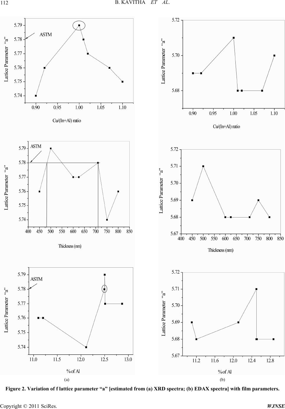
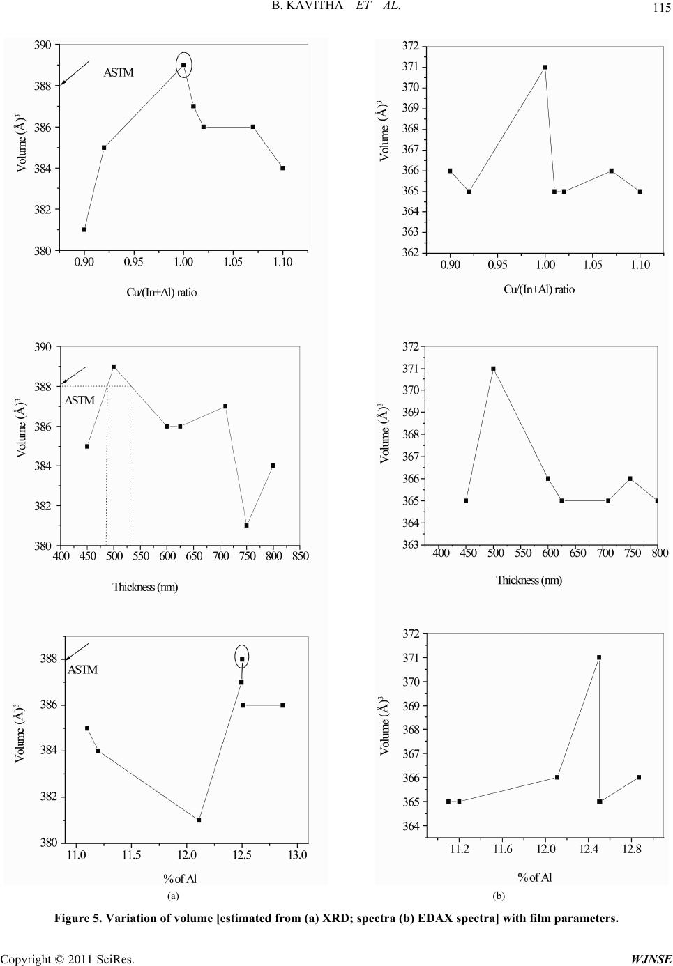
The volume of the unit cell has been found maximum
when Cu/(In + Al) ratio is 1 and the atomic % of Al is
about 12.5. The volume of the unit cell varies non-line-
arly with film thickness and approaches ASTM value
when film thickness is around 480 nm to 530 nm in CBD
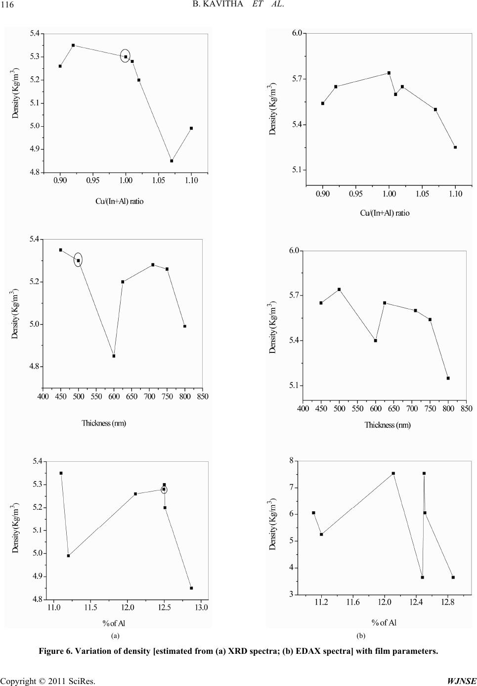
CIAS thin films (Figure 5). The estimated density of
CBD CIAS thin films lies in between the density of CIS
[5.77 Kg/m3] and CAS [4.77 Kg/m3]. The average den-
sity 5.27 Kg/m3 may be considered as the density of CIAS
thin films and this value is found when the Cu/(In + Al)
is unity, film thickness is 500 nm and the atomic % of Al
is 12.5 (Figure 6).
It has been found that the lattice constants, tetragonal
distortion, volume of the unit cell and density of CIAS
are in agreement with ASTM values when the film is
stoichiometric in nature (Cu/(In + Al) is 1, Al% is 12.5)
with film thickness in the range 500 - 710 nm.
4. Conclusions
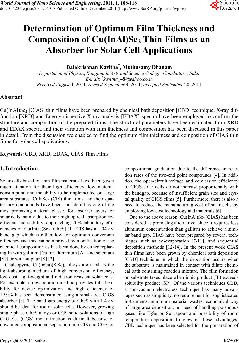
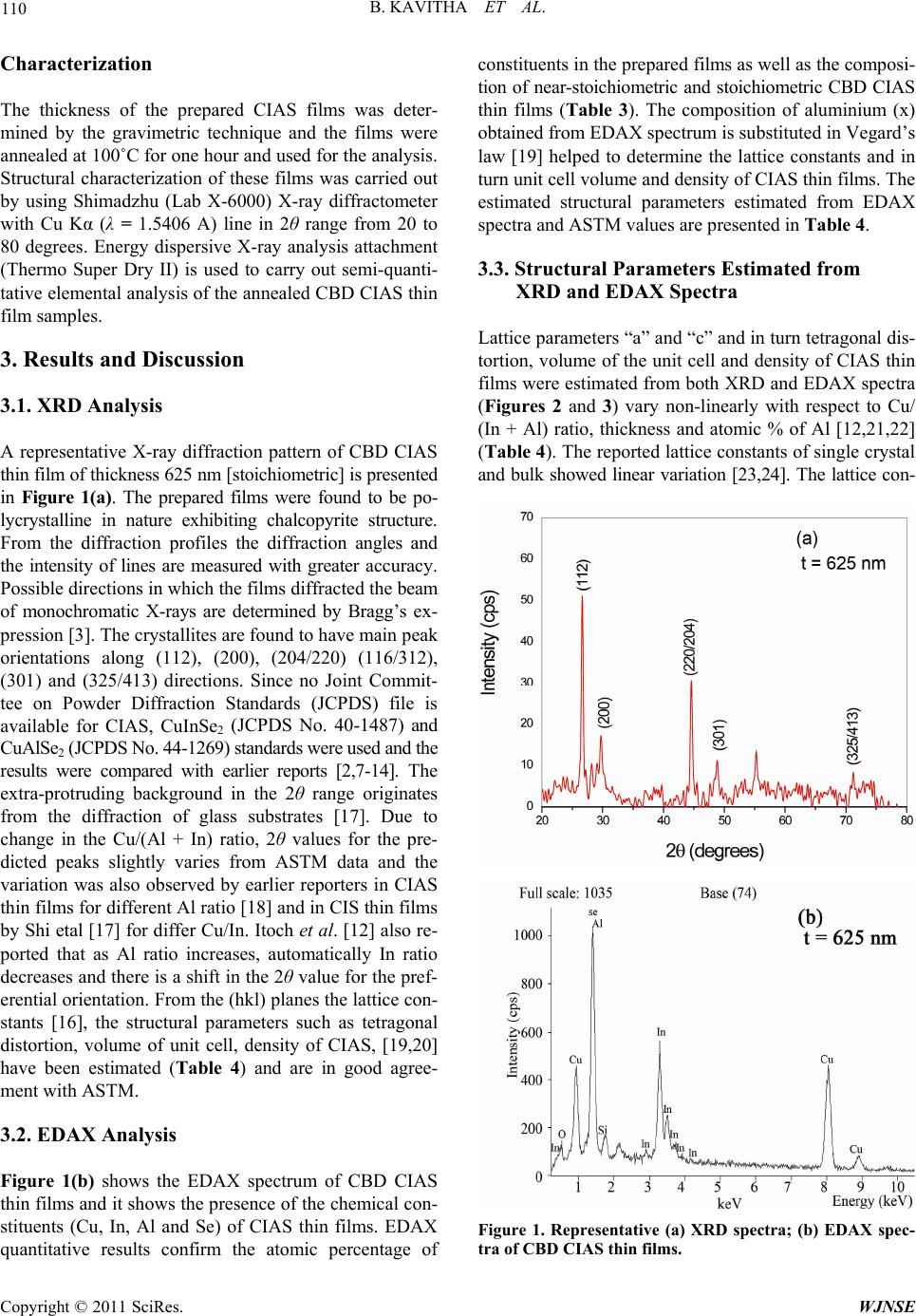
CIAS thin films have been prepared by CBD technique.
XRD and EDAX spectra have been employed to confirm
the structure and composition of the prepared films. The
structural parameters have been estimated from XRD and
EDAX spectra. From the estimated values suitable Cu/
(In + Al), % of Al and film thickness has been identified
for solar cell applications.
5. Acknowledgements
The authors are grateful to the Secretary, Principal and
Head of the Department of Physics, Kongunadu Arts and
Science College, Coimbatore for their excellent encour-
agement and support. One of the authors (B.K) is grate-
ful to express her thanks to Jawaharlal Nehru Memorial
Fund for financial support.
6. References
[1] M. A. Contreras, K. Ramanathan, J. AbuShama, F. Hasoon,
D. L. Young, B. Egas and R. Noufi, “Diode Characteris-
tics in State-of-the-Art ZnO/CdS/Cu(In1–xGax)Se2 Solar
Cells,” Progress Photovoltaics: Research and Applica-
tions, Vol. 13, No. 3, 2005, pp. 209-216.
doi:10.1002/pip.626
[2] S. Marsillac, P. D. Paulson, M. W. Haimbodi and W. N. Sha-
farman, “High-Efficiency Solar Cells Based on Cu(InAl)Se2
Thin Films,” Applied Physics Letters, Vol. 81, No. 7, 2002,
pp. 1350-1352.
[3] I. L. Repins, et al., “Comparison of Device Performance
and Measured Transport Parameters in Widely-Varying
Cu(In,Ga) (Se,S) Solar Cells,” Progress Photovoltaics: Re-
search and Applications, Vol. 14, No. 1, 2006, pp. 25-30.
doi:10.1002/pip.654
[4] K. Reddy, I. Forbes, R. Miles, M. Carter and P. Dutta,
Growth of High-Quality CuInSe2 Films by Selenising
Sputtered Cu-In Bilayers Using a Closed Graphite Box,”
Materials Letters, Vol. 37, No. 1-2, 1998, pp. 57-62.
doi:10.1016/S0167-577X(98)00066-4
[5] R. Herberholz, V. Nadenau, U. Rühe, C. Köble, H. W. Schock
and B. Dimmler “Prospects of Wide-Gap Chalcopyrites
for Thin Film Photovoltaic Modules,” Solar Energy Ma-
terials and Solar Cells, Vol. 49, No. 1-4, 1997, pp. 227-
237. doi:10.1016/S0927-0248(97)00199-2
[6] B. Munir, R. A. Wibowo, E. S. Lee and K. H. Kim, “One
Step Deposition of Cu(In1–xAlx)Se2 Thin Films by RF
Magnetron Sputtering,” Journal of Ceramic Processing
Research, Vol. 8, No. 4, 2007, pp. 252-255.
[7] P. D. Paulson, M. W. Haimbodi, S. Marsillac, R. W. Birk-
mire and W. N. Shafarman, “CuIn1–xAlSe2 Thin Films and
Solar Cells,” Journal of Applied Physics, Vol. 91, No. 12,
2002, pp. 10153-10156. doi:10.1063/1.1476966
[8] W. N. Shafarman, R. Klenk and B. E McCandless, “De-
vice and Material Characterization of Cu(InGa)Se2 Solar
Cells with Increasing Band Gap,” Journal of Applied Phy-
sics, Vol. 79, No. 9, 1996, pp. 7324-7328.
doi:10.1063/1.361431
[9] Y. Bharath Kumar Reddy and V. Sundara Raja, “Optical
and structural Properties of Co-Evaporated CuIn0.5Al0.5Se2
Thin Films,” Semiconductor Science and Technology,
Vol. 19, No. 8, 2004, pp. 1015-1019.
doi:10.1088/0268-1242/19/8/011
[10] Y. Bharath Kumar Reddy and V. Sundara Raja, “Prepara-
tion and Characterization of CuIn0.3Al0.7Se2 Thin Films
for Tandem Solar Cells,” Solar Energy Materials and
Solar Cells, Vol. 90, No. 11, 2006, pp. 1656-1665.
doi:10.1016/j.solmat.2005.09.002
[11] Y. Bharath Kumar Reddy and V. Sundara Raja, “Prepara-
tion and Characterization of CuIn0.75Al 0.2 5Se 2 Thin Films
by Co-Evaporation,” Physica B: Condensed Matter, Vol.
381, No. 1-2, 2006, pp. 76-81.
doi:10.1016/j.physb.2005.12.256
[12] E. Itoch, O. Saitoh, M. Kita, H. Nagamori and H. Oike,
“Growth and Characterization of Cu(InAl)Se2 by Vacuum
Evaporation,“ Solar Energy Materials and Solar Cells,
Vol. 50, No. 1-4, 1998, pp. 119-125.
doi:10.1016/S0927-0248(97)00132-3
[13] Dhananjay, J. Nagaraju and S. B. Krupanidhi, “Structural
and Optical Properties of CuIn1xAlxSe2 Thin Films Pre-
pared by Four-Source Elemental Evaporation,” Solid State
Communications, Vol. 127, No. 3, 2003, pp. 243-246.
doi:10.1016/S0038-1098(03)00389-2
[14] E. Halgand, J. C. Bernede, S. Marsillac and J. Kessler,
“Physico-Chemical Characterization of Cu(InAl)Se2 Thin
Film for Solar Cells Obtained by Selenization Process,”
Thin Solids Films, Vol. 480-481, No. 1, 2005, pp. 443-446.
doi:10.1016/j.tsf.2004.11.039
[15] M. Dhanam, P. K Manoj and R. R. Prabhu, “High Tem-
perature Conductivity in Chemical Bath Deposited Cop-
per Selenide Thin Films,” Journal of Crystal Growth, Vol.
280, No. 3-4, 2005, pp. 425-435.
doi:10.1016/j.jcrysgro.2005.01.111
B. KAVITHA ET AL.
118
[16] B. Kavitha and M. Dhanam, “Study of Chemical Bath
Deposited Cu(In,Al)Se2 Thin Films as an Alternate Can-
didate for Solar Cells,” Journal of Ceramic Processing
Research, Vol. 10, No. 5, 2009, pp. 652-656.
[17] Y. Shi, Z. Jin, C. Li, H. An and J. Qiu, “Effect of [Cu]/[In]
Ratio on Properties of CuInS2 Thin Films,” Applied Sur-
face Science, Vol. 252, No. 10, 2006, pp. 3737-3743.
doi:10.1016/j.apsusc.2005.05.055
[18] Y. Hamakawa, “Thin-Film Solar Cells: Next Generation
Photovoltaics and Its Applications,” Springer Series in
Photonics, Vol. 13, 2004, p. 244.
[19] M. Dhanam, R. Balasundarprabhu, S. Jayakumar, P. Gopa-
lakrishnan and M. D. Kannan, “Preparation and Study of
Structural and Optical Properties of Chemical Bath De-
posited Copper Indium Diselenide Thin Film,” Physica
Status Solidi (a), Vol. 191, No. 1, 2002, pp. 149-160.
[20] V. Bodnar, I. N. Tsyrelchuk and I. A. Victorov, “Prepara-
tion and Analysis of the CuAlxln1–xSe 2 Solid Solutions,”
Journal of Materials Science Letters, Vol. 13, No. 10,
1994, pp. 762-764. doi:10.1007/BF00461397
[21] J. López-García and C. Guillén, “CuIn1–xAlxSe2 Thin Films
Obtained by Selenization of Evaporated Metallic Precursor
Layers,” Thin Solid Films, Vol. 517, No. 7, 2009, pp. 2240-
2243. doi:10.1016/j.tsf.2008.10.095
[22] Y. Bharath Kumar Reddy, V. Sundarara Raja and B. Sreed-
har, “Growth and Characterization of CuIn1xAlxSe2 Thin
Films Deposited by Co-Evaporation,” Journal of Physics
D: Applied Physics, Vol. 39, No. 24, 2006, pp. 5124-
5132. doi:10.1088/0022-3727/39/24/005
[23] W. Gebicki, M. Igason, W. Zajac and R. Trykozko,
“Growth and Characterisation of CuAlxIn1–xSe2 Mixed
Crystals,” Journal of Physics D: Applied Physics, Vol. 23,
No. 7, 1990, pp. 964-966.
doi:10.1088/0022-3727/23/7/034
[24] H. Miyake and K. Sugiyamma, “Photoluminescence Cha-
racteristics of CuAlxIn1xSe2 Solid Solutions Grown by
Iodine Transport Technique,” Journal of Applied Physics,
Vol. 72, No. 8, 1992, pp. 3697-3702.
doi:10.1063/1.352314
[25] M. Varela, E. Bertran, J. Esteve and J. L. Morenza, “Crys-
talline Properties of Co-Evaporated CuInSe2 Thin Films,”
Thin Solid Films, Vol. 130, No. 1-2, 1985, pp. 155-164.
doi:10.1016/0040-6090(85)90304-9
Copyright © 2011 SciRes. WJNSE