Int'l J. of Communications, Network and System Sciences
Vol.3 No.1(2010), Article ID:1176,6 pages DOI:10.4236/ijcns.2010.31009
A Simple On-Chip Automatic Tuning Circuit for Continuous-Time Filter
Department of Electrical Engineering, National Sun Yat-Sen Uuniversity, Kaohsiung, Taiwan, China
E-mail: p923010026@student.nsysu.edu.tw
Received September 10, 2009; revised October 12, 2009; accepted November 17, 2009
Keywords: Automatic, Tuning, Voltage-Controlled Filter (VCF), Single-Time Constant (STC)
Abstract
A simple on-chip automatic frequency tuning circuit is proposed. The tuning circuit is modified from voltage-controlled filter (VCF) frequency tuning circuit. We utilize an operational transconductance amplifier and a capacitor to from a single-time constant (STC) circuit which can produce a controllable delay time clock to tune the frequency of the filter. It can efficiently reduce the deviations in the 3 dB bandwidth from the variations of PVT (Process, Voltage and Temperature). The design of the STC circuit is simpler than VCF and it has less chip area. The chip has been implanted using TCMC 0.35 μm CMOS technology and the power consumption is less than 9.05 mW.
1. Introduction
Analog continuous-time filters [1] are popular in various application, such as video and audio signal processing, ADC, mobile phone, hard disk reading channels, CDROM, etc. Recently, the Gm-C filters are widely used in the CMOS technology. The Gm-C filters have higher frequency and flexibility than other analog filter types. However, their performances vary with process and environment variations. The frequency response of analog continuous-time filters is determined by resistors, capacitors or transconductors. However, the process variation, temperature drift and aging, make the integrated RC time constants vary about 30% [2,3]. At extreme conditions, the maximum frequency response deviations could be up to 50% [4]. To achieve the desired filter performance, an on-chip automatic tuning scheme is usually required [5–14].
Many kinds of frequency automatic-tuning methods are derived from phase locked loop (PLL) for analog filters, such as sinusoidal oscillator based PLL tuning circuit, voltage-controlled filter (VCF) tuning circuit and etc [1,5,6,13]. The drawbacks of the sinusoidal oscillator based PLL tuning are large size and hard to design. As to the voltage-controlled filter tuning circuit, the power consumption is high and the reference clock needs to be a pure sine wave. According to the aforementioned, we try to make the tuning circuit have following advantages: simplicity, small chip area, good matching with the filter and less power consumption.
In the following sections, Section 2 presents the proposed tuning circuit and the Gm-C filter and the experimental results are discussed in Section 3. Section 4 summarizes the conclusions of this paper.
2. The Proposed Tuning Circuit and the Gm-C Filter
2.1. The Operation of Proposed Tuning Mechanism
Figure 1 shows the proposed tuning circuit scheme. Firstly, the frequency tuning circuit is modified from voltage-controlled filter (VCF) frequency tuning circuit. We replace VCF by a single-time-constant (STC) circuit and the input signal could be square wave. The function of STC is to produce a delay clock which the delay can be controlled. The phase difference will make the charge pump (CP) produce a control voltage. The phase difference is 45° between the reference clock and the output of the voltage comparator. The tuning circuit depends on the constant phase difference to tune the slave filter. Finally, it generates the control voltage after the voltage signal is filtered by the low pass filter (LPF).
Next, we discuss the STC circuit. The STC circuit consists of a tunable OTA, as shown in Figure 2, and a capacitor. We use the tunable OTA to simulate a variable resistance, and we obtain a STC circuit by connecting the OTA with a capacitor.

Figure 1. The block diagram of tuning circuit. (PD: Phase Detector, CP: Charge Pump, LPF: Low Pass Filter).

Figure 2. The STC circuit.
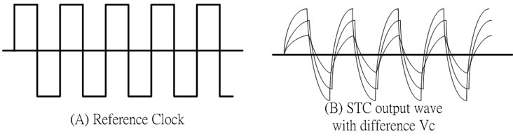
Figure 3. (A) Reference clock (B) STC output wave with three different Vc.
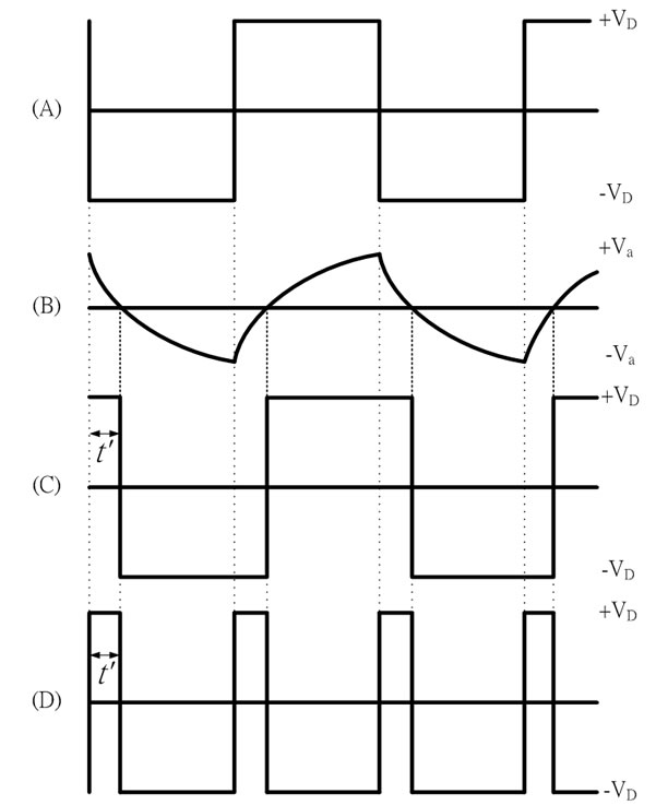
Figure 4. (A) Reference clock (B) The output of the STC circuit (C) The output of the voltage comparator (D) The output of the PD.
The transfer function of the STC is
 (1)
(1)
 (2)
(2)
If we input a reference clock, the STC will output a pseudo-triangular wave. The output wave of the STC circuit with three different control voltages Vc are shown in Figure 3.
When we input a reference clock with amplitude ± VD as shown in Figure 4(A), the STC circuit will output a pseudo-triangular wave with amplitude ± Va as shown in Figure 4(B). The pseudo-triangular wave is symmetrical with respect to the zero voltage. We will use a voltage comparator which is referenced at the zero voltage, so it will produce a clock with a delay time, t', as shown in Figure 4(C). We can find out the relation between the delay time and the time constant, τ, of the pseudo-triangular wave.
From Figure 4(B), it can be derived that the relation between t' and τ is:
 (3)
(3)

 (4)
(4)
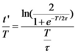
Figure 5. t'/T VS T/τ.
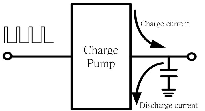
Figure 6. Charge and discharge current.

Figure 7. The structure of proposed tuning circuit ((1): STC circuit, (2): Voltage comparator, (3): Phase Detector, (4): Charge Pump, (5): Low Pass Filter).
Figure 5 is the curve of Equation (3). If we choose t'/T = 1/8, then α = 0.776. When T = 10MHz, the critical frequency of the STC is 7.76MHz.
Figure 6 shows a diagram of the charge and discharge current in CP. We set the charge current and discharge current with a ration 3:1. At charge balance, the reference frequency and STC output will be locked at 45° phase difference such that t'/T = 1/8. For the other, we adjust the delay time of the STC with a constant reference clock. The STC circuit is transferred to a square wave, as shown in Figure 4(C). We will detect the phase difference of two square waves by a phase detector, as shown in Figure 4(D). This wave is applied to the charge pump to adjust τ, as shown in Figure 6. At the output of the charge pump, the charge current is three times the discharge current. Because of electric balance, the delay time will be T/8.
2.2. The Structure of Proposed Tuning Circuit
Figure 7 shows the proposed circuit that is consisted of five sub circuits. The first part of the proposed circuit is the STC circuit. It consists of a tunable OTA [8] and a capacitor. We can find the transconductance of the OTA is:
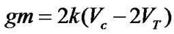 (5)
(5)
where k=0.5µnCoxW/L is the transconductance parameter, and µnCoxW and L are the mobility, oxide capacitance per unit area, channel width and length, respectively. VT is the threshold voltage, and Vc is the OTA’s control voltage. We can adjust the STC’s RC time by varying the OTA’s control voltage, Vc. It stands to reason that the tunable OTA’s design is easier than a VCF and the size is much smaller than a VCF. When the Reference Clock is applied to the STC circuit, a differential pseudo-triangular wave will be produced. If the control voltage is higher, the gm will be bigger. The charge and discharge
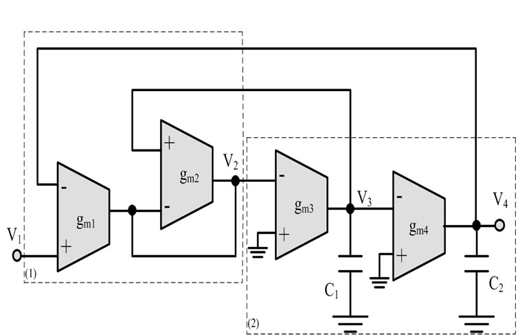
Figure 8. Two-order Gm-C biquad filter [12].
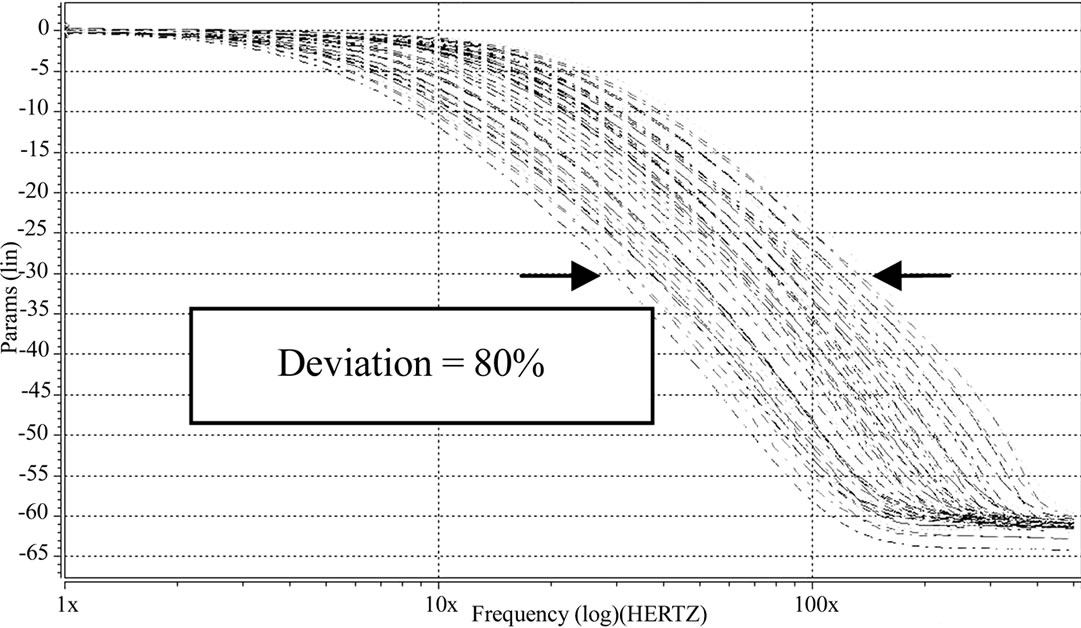
Figure 9. The 3-dB frequency variation in sixty corners (without tuning).

Figure 10. The 3-dB frequency variation in sixty corners (with tuning).
of the capacitor will be quicker. The phase difference between the output wave and the reference frequency will be smaller. Finally, the phase difference will be locked at the specified value.
The voltage comparator is composed of a V-I converter, a current comparator and an inverter, as shown in Figure 7(2). The delay of the voltage comparator is longer than the sum of these devices’ delay and the sum of these devices’ delay is shorter than a conventional high speed voltage comparator. Next, we want to detect the phase difference between the reference frequency and the output wave of the Inverter. We use a phase detector, which is constructed by an XNOR, as shown in Figure 7(3). Figure 7(4) is the charge pump (CP). The capacitor will be charged and discharged by current source. M36,M37, M38, M41 and M42 are three current mirrors. M37 and M38 will mirror M36’s current Ibias and Idischarge is equal to Ibias because M42’s size is almost three times as M41. Icharge is equal to 3Ibias. We set the charge current and discharge current with a ratio 3:1. At charge balance, the reference frequency and STC output will be locked at 45° phase difference. If the current source of the CP is large, the phase will be quickly locked. But the ripple will be large. To reduce the ripple, we use a low-pass filter (LPF) like in Figure 7(5).
2.3. The Gm-C Filter
Figure 8 shows a two-order Gm-C low-pass filter made by OTAs [12]. The cut-off frequency is 10 MHz by design. We will use this filter to prove our tuning circuit is working. The transfer function can be expressed as:
 (6)
(6)
where 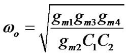 and
and .
.
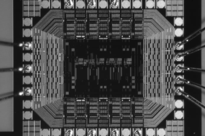
Figure 11. Die photo of the proposed circuit.
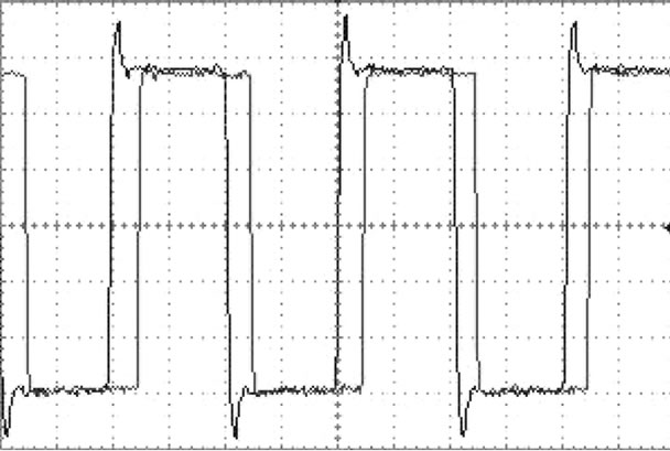
Figure 12. Reference clock and delay clock.
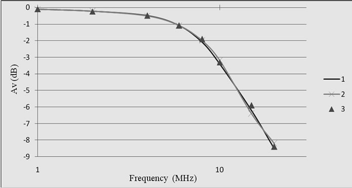
Figure 13. Filter frequency responses in three samples.
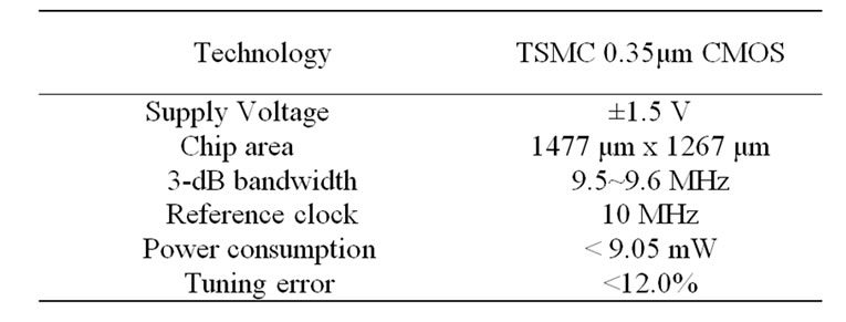
Table 1. Filter performance parameter.
3. Simulation and Experimental Results
The simulation is carried out using HSPICE with TSMC 0.35um CMOS models. There are five modes of SPICE model, TT, FF, SS, FS and SF. These five models are used to simulate the CMOS process variation. Figure 9 shows the 3-dB frequency variation in sixty corners. The sixty corners include five CMOS models(TT、FF、SS、FS、SF), three voltages (±1.35 V、±1.5 V、±1.65 V) and four temperatures (-20℃, 0℃, 25℃, 70℃).
Without the tuning circuit, the maximum variation of the 3-dB frequency in sixty corners is about 80%.
Figure 10 shows the simulation result of the low-pass Gm-C filter with the tuning circuit in sixty corners. The maximum variation of the 3-dB frequency in sixty corners is about 12%. Comparing Figure 9 with Figure 10, we find that the frequency tuning circuit can reduce 3-dB frequency variation from 80% to 12%.
The proposed circuit is implemented by 0.35 μm TSMC 2P4M CMOS process and its die photograph is shown in Figure 11. The chip area is 1477 μm x 1267 μm. We have measured the delay clock to check if the tuning circuit operates correctly. Then we measure filter output to check the bandwidth. Figure 12 shows reference clock and delay clock. Figure 13 shows the filter frequency response in three samples.
The measured performance of the filter are shown in Table 1. The performance of the proposed circuit was good, confirming the expectation that the tuning circuit can reduce the tolerance. Also the power consumption is small and less than 9.05 mW.
4. Conclusions
This paper has presented a simple automatic tuning circuit, which is applied to a ± 1.5 V 10 MHz low-pass Gm-C filter. The greatest advantage of the proposed tuning circuit is compact and easy to be realized without designing a complicated voltage controlled oscillator. The size of the tuning circuit is another advantage. The chip area is only about 0.12 x 0.14 mm2. From the results, the frequency tuning circuit can reduce the frequency tolerance efficiently. All the circuits are designed based on the TSMC 0.35 μm 2P4M CMOS process technology.
5. Acknowledgment
The authors would like to thank the national chip implementation center (CIC) for the chip fabrication.
6. References
[1] Y. P. Tsividis, “Integrated continuous-time filter design - an overview,” IEEE Journal Solid-State Circuits, Vol. 29, No. 3, pp. 166–176, March 1994.
[2] M. Abo and P. R. Gray, “A 1.5 V, 10-bit, 14 MS/s CMOS pipeline analog-to-digital converter,” IEEE Journal SolidState Circuits, Vol. 34, No. 5, pp. 599–606, May 1999.
[3] L. Maurer, W. Schelmbauer, H. Pretl, B. Adler, A. Springer, and R. Weigel, “On the design of a continuous-time channel select filter for aZero-IF UMTS receiver,” IEEE Conference Vehicular Technology, Vol. 1, pp. 650–654, May 2000.
[4] M. Durham, W. Redman-White, and J. B. Hughes, “High-linearity continuous-time filter in 5-V VLSI CMOS,” IEEE Journal Solid-State Circuits, Vol. 27, No. 9, pp. 1270–1276, September 1992.
[5] J. Silva-Martinez, M. S. J. Steyaert, and W. Sansen, “A 10.7-MHz 68-dB SNR CMOS continuous-time filter with on-chip automatic tuning,” IEEE Journal Solid-State Circuits, Vol. 27, No. 12, pp. 1843–1853, December 1992.
[6] T. H. Teo, E.-S. Khoo, and D. Uday, “Fifth order low-pass transitional Gm-C filter with relaxation oscillator frequency tuning circuit,” IEEE Conference Electron Devices and Solid-State Circuits, pp. 229–232, December 2003.
[7] D. Johns and K. Martin, “Analog integrated circuit design,” John Wiley & Sons on Canada, 1997.
[8] S. Szczepanski and S. Koziel, “A 3.3 V linear fully balanced CMOS operational transconductance amplifier for high-frequency applications,” IEEE Conference Circuits and Systems for Communications, pp. 38–41, June 2002.
[9] H. Traff, “Novel approach to high speed CMOS current comparators,” Electronics Letters, Vol. 28, No. 3, pp. 310–312, January 1992.
[10] H. T. Bui, A. K. Al-Sheraidah, Y. K. Wang, “New 4-transistor XOR and XNOR designs,” IEEE Asia Pacific Conference ASICs, pp. 25–28, August 2000.
[11] W. Rhee, “Design of high-performance CMOS charge pumps in phase-locked loops,” IEEE International Symposium Circuits and Systems, Vol. 2, pp. 545–548, June 1999.
[12] K. Su, “Analog filters,” Second Edition, Kluwer Academic Publishers, 2001.
[13] Y. P. Tsividis, “Design considerations for high-frequency continuous-time filters and implementation of an antialiasing filter for digital video,” IEEE Journal SolidState Circuits, Vol. 25, No. 6, pp. 1368–1378, December 1990.
[14] V. Agarwal and S. Sonkusale, “A PVT independent subthreshold Constant-Gm stage for very low frequency applications,” IEEE International Symposium Circuits and Systems, pp. 2909–2912, May 2008.