Journal of Modern Physics
Vol.4 No.3(2013), Article ID:28655,5 pages DOI:10.4236/jmp.2013.43048
Effect of Deposition Temperature on the FTIR Absorbance of Zinc Oxide Thin Films Produced by MOCVD
Department of Physics, Federal University of Technology, Owerri, Nigeria
Email: *uesmbams@gmail.com
Received December 27, 2012; revised January 29, 2013; accepted February 9, 2013
Keywords: ZnO Thin Films; MOCVD; Impurities; FTIR Absorbance; Applications
ABSTRACT
Metalorganic chemical vapour deposition (MOCVD) method was used to deposit zinc oxide thin films on soda-lime glass substrates at temperatures of 330˚C, 360˚C, 390˚C and 420˚C, using zinc acetate as the precursor. Compressed air was used as the carrier gas at a flow rate of 2.5 dm3 per minute. Each deposition was carried out for two hours under atmospheric pressure. FTIR measurements were subsequently made on the produced thin films to determine their structure and trend with deposition temperatures. The measurements showed the presence of lingering functional groups of organic, oxide and nitride origin, which prominently moderated the natural vibrational modes of the material within their respective affiliate wavenumbers, as well as three slight but evident trends in absorbance peaks, cut-off wavelength, and the existence of the functional groups with temperature. The produced materials are expected to be useful for enhanced solar cells, triggering sensor devices, p-doped zinc oxide, etc.
1. Introduction
Zinc oxide is a common material that continues to assume versatile technological prominence unabated [1-6]. Zinc oxide thin films are strategically useful as anti-reflectors, solar cells and transparent semiconductors which are invaluable in optoelectric display units, transparent contacts, light emitting diodes, photosensors, gas sensors, piezoelectric and spintronic materials, etc. Their high optical transmittance (over 80%), energy bandgap (3.2 - 3.4 eV), crystal structure, and good optical and thermal stability make them especially invaluable for these applications [7-11]. Added to these are its tribological properties that extend its use to the world of lubricants and friction controls [12-14].
A major setback in the use of zinc oxide in microelectronics, however, is the difficulty in realizing its p-type material, and where this has been achieved, it is often unstable [15-19]. Several theoretical and experimental proofs have been adduced for the anomaly in relation to the n-type material, among which are the omnipresence of interstitial hydrogen, and the presence of carbon, oxygen and nitrogen with their functional groups [16,20-24]. The moderating influence of these on zinc oxide with their respective vibrational modes bears much on its electrical properties and morphology [21-25]. However, phosphorus, nitrogen and a few other desirable impurities have been used to effectively produce the p-type material [18,19,23].
Fourier Transform Infrared (FTIR) spectroscopy is a simple, non-destructive technique used to identify all the elements in a material [26-28]. It makes use of the fact that spectral display of any given molecule is unique to it, and any foreign atom within its structure shows up itself by its moderating influence on the spectrum at its characteristic position [28-30]. This property makes FTIR a versatile tool for characterization of thin films and other substances [26].
2. Experimental Procedure
In this work, the metalorganic chemical vapour deposition (MOCVD) method was used to deposit zinc oxide thin films on soda-lime glass substrates at temperatures of 330˚C, 360˚C, 390˚C and 420˚C (See Figure 1). The precursor used was zinc acetate dihydrate particles at a flow rate of 2.5 dm3 per minute, with compressed air as the carrier gas, while the working pressure was atmospheric. Each coating was done for two hours.
Each thin film was then subjected to FTIR analysis using a Buck Scientific Model 500 IR Spectrophotometer. The FTIR absorbance of the samples were measured in the wavenumber interval of 2500 cm−1 to 3800 cm−1. The actual measurements made by the machine were the IR transmittance of the samples within the chosen wavelength range, and then these were translated to IR ab-
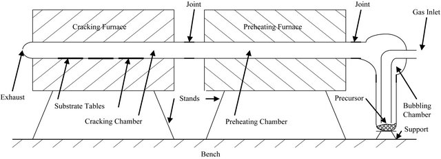
Figure 1. Schematic of our two-chamber MOCVD set-up.
sorbance by the formula
 (1)
(1)
The measurements were made at room temperature and an uncoated substrate was used as the blank measurement and control. The results were subsequently analyzed and compared vis-à-vis the deposition temperatures.
3. Results and Discussion
The FTIR absorbance spectra of the ZnO thin films produced are shown in Figures 2-5. The spectra obtained are all similar in shape and character, save for minor alterations apparently resulting from the different deposition temperatures and the spectral moderation by lingering assays [30]. To begin with, the absorption spectra are skew-symmetric, and this is possibly due to the moderating influence of assays like hydrogen, carbon, oxygen and nitrogen, whose presence are registered by the premature peaks occurring about 2825 cm−1 to 3020 cm−1 within the spectra, with their attendant moderating Gaussian peaks [29]. These elemental inclusions arise from the precursor make up and the carrier gas, and impose a considerable influence on the structure of the ZnO thin films produced [19,20,22]. The asymmetric spectral displays uniformly peaked at 3400 cm−1, and remnant O-H and C-H bonds and ZnO vacancies are believed to be responsible for the skew [22,28,29]. In fact the exact impact of each remnant functional group or factor requires complete analysis for the exact configuration of the thin film to be specified [22,28-30].
On the basis of the deposition temperature, the results show minute but significant trends in three aspects viz: absorption cut-off edge, absorption peaks and the Gaussian noise. The absorbance spectra cut the wavenumber axes respectively at 3745 cm−1 for the 330˚C deposition, 3735 cm−1 for 360˚C, 3712 cm−1 for 390˚C, and 3709

Figure 2. FTIR spectra and gaussian peaks at deposition temperature of 330˚C.

Figure 3. FTIR spectra and gaussian peaks at deposition temperature of 360˚C.
cm−1 for 420˚C. These respectively translate to wave lengths of 267 µm for the 330˚C deposition, 268 µm for 360˚C, 269 µm for 370˚C, and 270 µm for 420˚C. Thus the effect is small but quite trending, cutting off at a minutely higher wavelength as the deposition temperature increases. The absorption peaks observed were 25.5 × 10⁻³ for deposition at 330˚C, 25.5 × 10⁻³ at 360˚C, 24.7 × 10⁻³ at 390˚C, and 23.1 × 10⁻³ at 420˚C, thereby showing

Figure 4. FTIR spectra and gaussian peaks at deposition temperature of 390˚C.

Figure 5. FTIR spectra and gaussian peaks at deposition temperature of 420˚C.
a slightly decreasing absorption peak with increasing deposition temperature.
Table 1 highlights these variations. The effects of the embedded functional groups were also observed to reduce with increasing deposition temperature, as can be seen from the spectral displays. The observation is even ordinarily logical, since the lingering H, C, and possibly O and N groups as well as defects should progressively crack off as temperature increases [2,5,10]. Much of the enduring peaks at higher temperatures are hence envisaged to be due mainly to oxide and nitride groups [19].
The discussion so far forebears some obvious advantages in the appropriate choice of deposition temperature to produce the desired brand of the semiconductor material. The p-doping of the substance with nitrogen, which has been reported an arduous task, could most likely be easily realized by this MOCVD method at higher temperatures [2,19]. The reduction in the absorption peak at higher deposition temperatures is also advantageous, as it makes more infrared rays transmissible through the material. The slight variation in the cut-off frequencies with varying deposition temperatures can also be employed to produce components with strategic triggering points as desired. Zinc oxide solar cells can also be produced to
Table 1. Effect of deposition temperature on FTIR spectral peak and cut-off wavelength.

work from the cut-off IR point through visible to the UV range, thereby making the material more versatile.
4. Conclusions
In this work the FTIR of zinc oxide thin films deposited at various temperatures on soda-lime glass substrate was reported. The thin films were deposited by the MOCVD process from zinc acetate precursor. The FTIR spectra showed the inclusion of some functional groups, supposedly comprising H, C, O, and N ligands, as well as defect in the zinc oxide thin films, as in highlighted literature [22,26,28-30]. The effect of the included functional groups was observed to decrease with increasing deposition temperature. Also, the absorption peaks of the FTIR spectra were observed to decrease slightly with increasing deposition temperature. In the case of the IR absorbance cut-off wavelength, there were slight increases with increasing deposition temperatures.
Applications derivable from these findings include the possibility of realizing nitrogen-doped p-type zinc oxide at elevated deposition temperatures, inclusion of some IR range in the manufacture of zinc oxide solar cells, fabrication of strategic triggering sensor materials with zinc oxide, general microelectronics, etc.
5. Acknowledgements
The authors are grateful to the following for their varied assistance in carrying out the work: Materials Science Laboratory, Department of Physics, Obafemi Awolowo University, Ile-Ife, Nigeria; Department of Chemistry, Obafemi Awolowo University, Ile-Ife, Nigeria; and Department of Physics, Federal University of Technology, Owerri, Nigeria.
REFERENCES
- Access Data, “Database of Select Committee on GRAS Substances, (SCOGS) Reviews,” 2009. http://www.accessdata.fda.gov/scripts/fcn/fcnDetailNavigation.cfm?rpt=scogsListing&id=372
- U. S. Mbamara, O. O. Akinwunmi, E. I. Obiajunwa, I. A. O. Ojo and E. O. B. Ajayi, “Deposition and Characterization of N-doped ZnO Thin Films by MOCVD Using Zinc Acetate—Ammonium Acetate Precursor,” Journal of Modern Physics, Vol. 3, No. 8, 2012, pp. 652-659. doi:10.4236/jmp.2012.38089
- M. D. McCluskey and S. J. Jokela, “Sources of n-Type Conductivity in ZnO,” Physica B, Vol. 401-402, 2007, pp. 355-357. doi:10.1016/j.physb.2007.08.186
- Ü. Özgür, Y. I. Alivov, C. Liu, A. Teke, M. A. Reshchikov, S. Doğan, V. Avrutin and S. J. Cho, “A Comprehensive Review of ZnO Materials and Devices,” Journal of Applied Physics, Vol. 98, No. 4, 2005, Article ID: 041301. doi:10.1063/1.1992666
- D. Scarano, S. Bertarione, F. Cesano, J. G. Vitillo and A. Zecchina, “Plate-like ZnO Microcrystals: Synthesis and Characterization of a Material Active toward H Adsorption,” Catalysis Today, Vol. 116, No. 3, 2006, pp. 433- 438. doi:10.1016/j.cattod.2006.05.062
- D. Look, “Recent Advances in ZnO Materials and Devices,” Materials Science and Engineering: B, Vol. 80, No. 1-3, 2001, pp. 383-387. doi:10.1016/S0921-5107(00)00604-8
- H. T. Wang, B. S. Kang, F. Ren, L. C. Tien, P. W. Sadik, D. P. Norton, S. J. Pearton and J. Lin, “Hydrogen-Selective Sensing at Room Temperature with ZnO Nanorods,” Applied Physics Letters, Vol. 86, No. 24, 2005, Article ID: 243503. doi:10.1063/1.1949707
- Science Daily, “New Small-Scale Generator Produces Alternating Current by Stretching Zinc Oxide Wires,” Science Daily, 2008. http://www.sciencedaily.com/releases/2008/11/081109193342.html
- A. C. Mofor, A. El-Shaer, A. Bakin, A. Waag, H. Ahlers, U. Siegner, S. Sievers and M. Albrecht, “Magnetic Property Investigations on Mn-Doped ZnO Layers on Sapphire,” Applied Physics Letters, Vol. 87, No. 6, 2005, Article ID: 062501. doi:10.1063/1.2007864
- M. D. McCluskey, S. J. Jokela, K. K. Zhuravlev, P. J. Simpson and K. G. Lynn, “Infrared Spectroscopy of Hydrogen in ZnO,” Applied Physics Letters, Vol. 81, No. 20, 2002, pp. 3807-3809. doi:10.1063/1.1520703
- T. Ohgaki, N. Ohashi, S. Sugimura, H. Ryoken, I. Sakaguchi, Y. Adachi and H. Haneda, “Positive Hall Coefficients Obtained from Contact Misplacement on Evident n-type ZnO Films and Crystals,” Journal of Materials Research, Vol. 23, No. 9, 2008, pp. 2293-2295. doi:10.1557/jmr.2008.0300
- S. V. Prasad, S. D. Walck and J. S. Zabinski, “Microstructural Evolution in Lubricious ZnO Films Grown by Pulsed Laser Deposition,” Thin Solid Films, Vol. 360, No. 1-2, 2000, pp. 107-117.
- J. S. Zabinski, J. Corneille, S. V. Prasad, N. T. McDevitt and J. B. Bultman, “Lubricious Zinc Oxide Films: Synthesis, Characterization and Tribological Behavior,” Journal of Materials Science, Vol. 32, No. 20, 1997, pp. 5313- 5319. doi:10.1023/A:1018614811131
- Z. Chai, X. Lu and D. He, “Atomic Layer Deposition of ZnO Films: Effects of Nanocrystalline Characteristics on Tribological Performance,” Surface and Coatings Technology, Vol. 207, 2012, pp. 361-366.
- X. Li, B. Keyes, S. Asher, S. B. Zhang, S. Wei, T. J. Coutts, S. Limpijumnong and C. G. Van de Walle, “Hydrogen Passivation Effect in N-doped ZnO Thin Films,” Applied Physics, Vol. 86, 2005, Article ID: 122107. doi.org/10.1063/1.1886256
- D. C. Look and B. Claflin, “p-Type Doping and Devices Based on ZnO,” Physica Status Solidi (b), Vol. 241, No. 3, 2004, pp. 624-630. doi:10.1002/pssb.200304271
- D. C. Look, B. Claflin, Y. I. Alivov and S. J. Park, “The Future of ZnO Light Emitters,” Physica Status Solidi (a), Vol. 201, No. 10, 2004, pp. 2203-2212. doi:10.1002/pssa.200404803
- X. Chen, Z. Zhang, B. Yao, M. Jiang, S. Wang, B. Li, C. Shan, L. Liu, D. Zhao and D. Shen, “Effect of Compressive Stress on Stability of N-doped p-type ZnO,” Applied Physics, Vol. 99, No. 9, 2011, Article ID: 091908. doi.org/10.1063/1.3631677
- C. G. Van de Walle and J. Neugebauer, “First-principles Calculations for Defects and Impurities: Applications to III-nitrides,” Journal of Applied Physics, Vol. 95, No. 8, 2004, pp. 3851-3879. doi:10.1063/1.1682673
- C. G. Van de Walle, “Theory of Hydrogen-Related Levels in Semiconductors and Oxides,” 2012. http://www.mrl.ucsb.edu/~vandewalle/IEDM120605_pdf
- J. Robertson, R. Gillen and S. J. Clark, “Advances in Understanding of Transparent Conducting Oxides,” Thin Solid Films, Vol. 520, No. 10, 2012, pp. 3714-3720. doi.org/10.1016/j.tsf.2011.10.063
- S. Limpijumnong, X. Li, S. Wei and S. B. Zhang, “Substitutional Diatomic Molecules NO, NC, CO, N2, and O2: Their Vibrational Frequencies and Effects on p-Doping of ZnO,” Applied Physics Letters, Vol. 86, No. 21, 2005, Article ID: 211910. doi:10.1063/1.1931823
- G. A. Shi, M. Saboktakin, M. Stavola and S. J. Pearton, “Hidden Hydrogen in As-grown ZnO,” Applied Physics Letters, Vol. 85, No. 23, 2004, pp. 5601-5603. doi.org/10.1063/1.1832736
- X. Li, S. E. Asher, B. M. Keyes, H. R. Moutinho, J. Luther and T. J. Coutts, “p-Type ZnO Thin Films Grown by MOCVD,” NREL/CP-520-37378, 2005.
- C. G. Van de Walle, “Hydrogen as a Cause of Doping in Zinc Oxide,” Applied Physics Letters, Vol. 85, No. 5, 2000, pp. 1012-1015. doi:10.1103/PhysRevLett.85.1012
- D. S. Kendall, “Infrared Spectroscopy of Coatings,” In: A. A. Tracton, Ed., Coatings Technology Handbook, 3rd Edition, CRC Press, Boca Raton, 2005. doi:10.1201/9781420027327.ch8
- W. Jacob, A. Keudell and T. Schwarz-Selinger, “Infrared Analysis of Thin Films: Amorphous, Hydrogenated Carbon on Silicon,” Brazilian Journal of Physics, Vol. 30, No. 3, 2000.
- B. M. Keyes, L. M. Gedvilas, X. Li and T. J. Coutts, “Infrared Spectroscopy of Polycrystalline ZnO and ZnO:N Thin Films,” Journal of Crystal Growth, Vol. 281, No. 2-4, 2005, pp. 297-302. doi:10.1016/j.jcrysgro.2005.04.053
- D. Scarano, S. Bertarione, G. Spoto, A. Zecchina and C. Oter o Area´n, “FTIR Spectroscopy of H, CO, and Methane Adsorbed and Co-adsorbed on Zinc Oxide,” Thin Solid Films, Vol. 400, No. 1-2, 2001, pp. 50-55. doi.org/10.1016/S0040-6090(01)01472-9
- J. Coates, “Interpretation of Infrared Spectra, a Practical Approach,” In: R. A. Meyers, Ed., Encyclopedia of Analytical Chemistry, John Wiley & Sons Ltd, Chichester, 2000, pp. 10815-10837.
NOTES
*Corresponding author: uesmbams@gmail.com